1
PS2011C 09/22/04
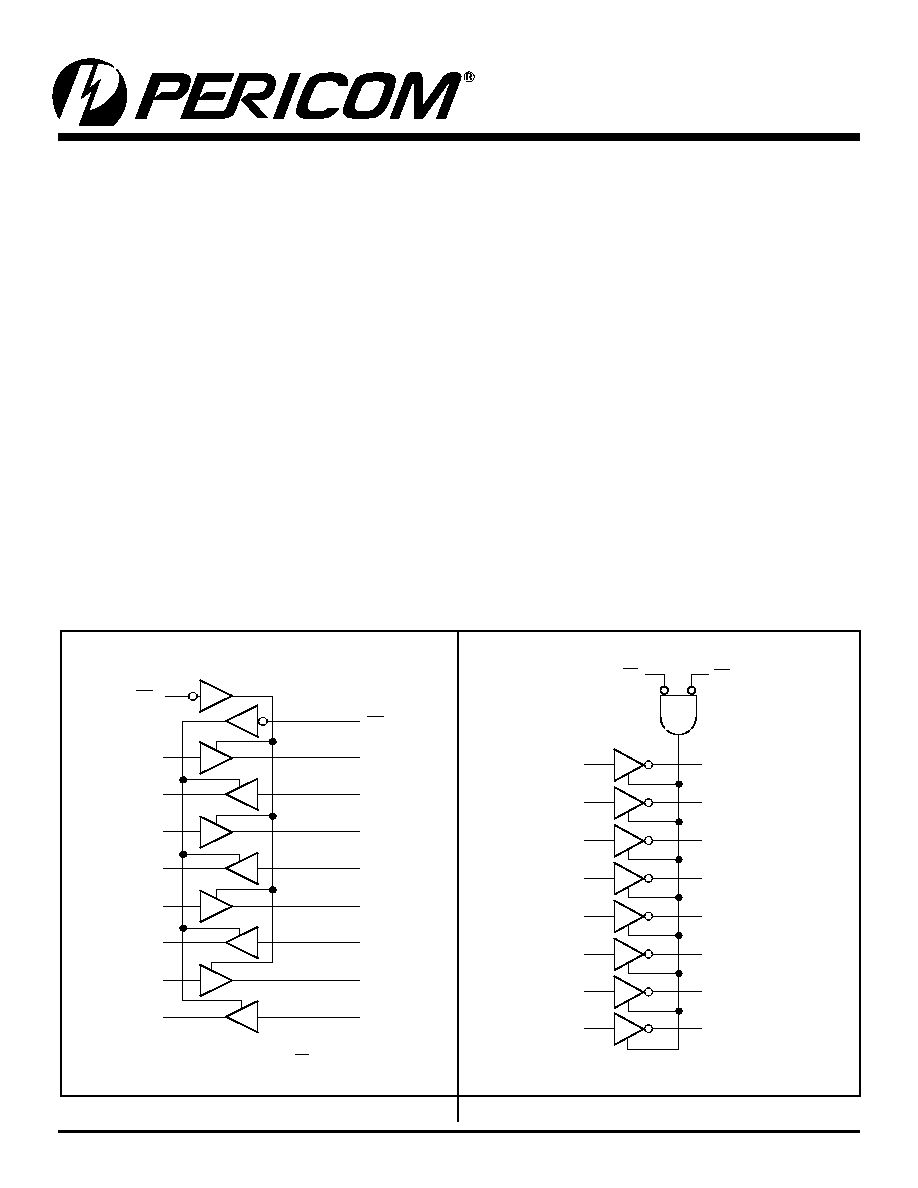
Block Diagrams
PI74FCT244/2244T
PI74FCT541/2541T
Description
Pericom Semiconductor's PI74FCT244T/541T and P174FCT2244/
2541T are 8-bit wide driver circuits, designed to be used in
applications requiring high-speed and high-output drive. Ideal
applications would include bus drivers, memory drivers, address
drivers, and system clock drivers.
The PI74FCT541 and 2541T provide similar driver capabilities,
but have their pins physically grouped by function. All inputs are
located on one side of the package, while outputs are on the opposite
side, allowing for a much simpler and denser board layout.
All PI74FCT2XXX devices have a built-in 25 series resistor on
all outputs to reduce noise because of reflections, thus eliminating
the need for an external terminating resistor.
Features
∑ PI74FCT244/541T and PI74FCT2244/2541T are pin
compatible with bipolar Fast Series at a higher speed and
lower power consumption
∑ 25 series resistor on all outputs (FCT2XXX only)
∑ TTL input and output levels
∑ Low ground bounce outputs
∑ Extremely low static power
∑ Hysteresis on all inputs
∑ Industrial operating temperature range: ≠40∞C to +85∞C
∑ Packaging (Pb-free & Green available):
≠ 20-pin 173-mil wide plastic TSSOP (L)
≠ 20-pin 209-mil wide plastic SSOP (H)
≠ 20-pin 150-mil wide plastic QSOP (Q)
≠ 20-pin 150-mil wide plastic TQSOP (R)
≠ 20-pin 300-mil wide plastic SOIC (S)
∑ Device models available upon request
OE
A
DA
0
OB
0
OB
1
DA
1
OB
2
DA
2
OB
3
DA
3
OA
0
DB
0
OE
B
*
OA
1
DB
1
OA
2
DB
2
OA
3
DB
3
*
OE
B
for 244T,
OE
A
D
0
O
0
OE
B
D
1
O
1
D
2
O
2
D
3
O
3
D
4
D
5
O
5
D
6
O
6
D
7
O
7
O
4
Fast CMOS Octal Buffer/Line Drivers
PI74FCT244T/2244T
PI74FCT541T/2541T
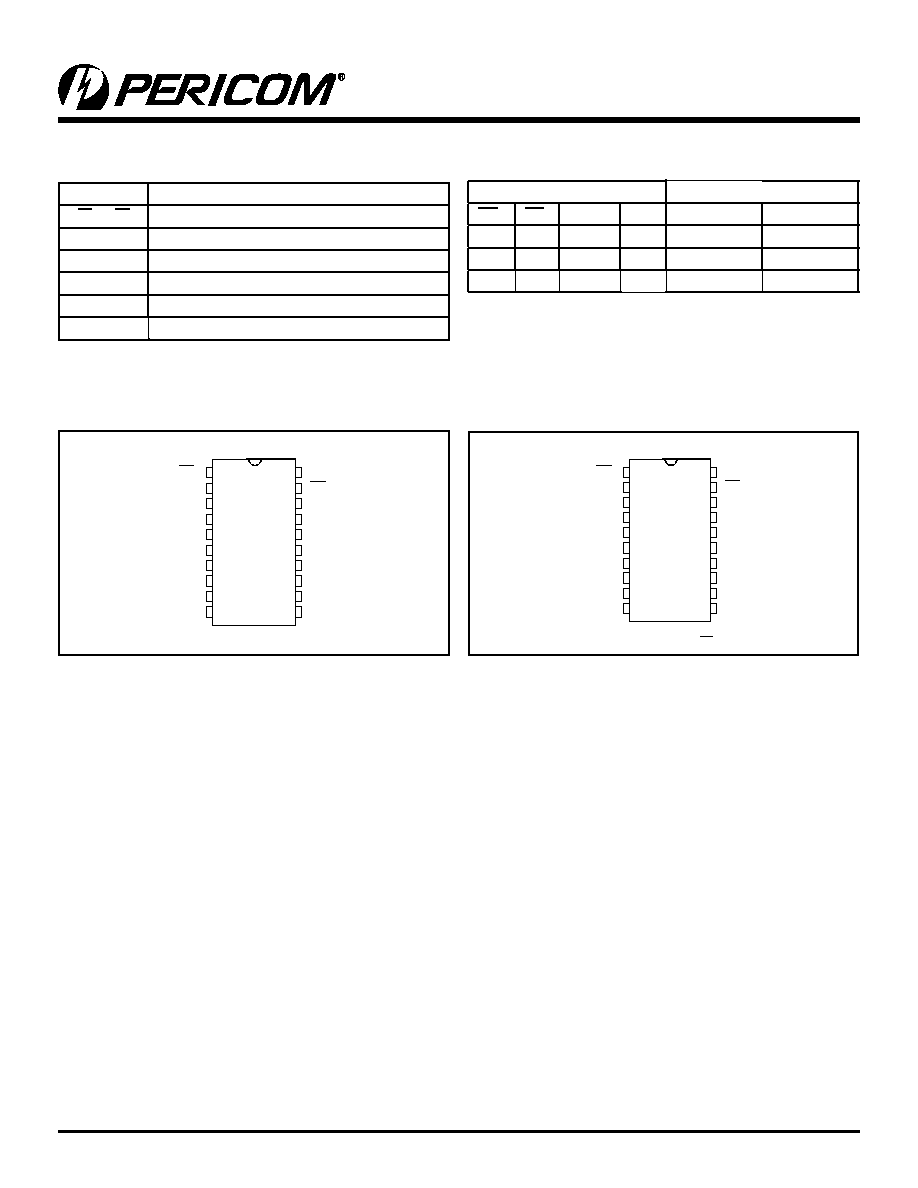
2
PS2011D 09/22/04
PI74FCT244T/2244T
PI74FCT541T/2541T
Octal Buffer/Line Drivers
Product Pin Description
Pin Name
Description
OEA, OEB
3-State Output Enable Inputs (Active LOW)
OEB
(1)
3-State Output Enable Input (Active HIGH)
Dxx
Inputs
Oxx
Outputs
GND
Ground
V
CC
Power
Truth Table
Inputs
(1)
Outputs
(1)
OE
A
OE
B
OE
B
(2)
D
244
541
L
L
H
L
L
L
L
L
H
H
H
H
H
H
L
X
Z
Z
Note:
1. H = High Voltage Level, X = Don't Care, L = Low
Voltage Level, Z = High Impedance
2. OE
B
for 241 only.
PI74FCT540/541/2541T Pin Configuration
PI74FCT241/2241/244/2244T Pin Configuration
1
2
3
4
5
6
7
8
9
10
20
19
18
17
16
15
14
13
12
11
OE
A
DA
0
OB
0
DA
1
OB
1
DA
2
OB
2
DA
3
OB
3
GND
Vcc
OE
B
OA
0
DB
0
OA
1
DB
1
OA
2
DB
2
OA
3
DB
3
20-Pin
H20
L20
P20
Q20
R20
S20
1
2
3
4
5
6
7
8
9
10
20
19
18
17
16
15
14
13
12
11
OE
A
D
0
D
1
D
2
D
3
D
4
D
5
D
6
D
7
GND
Vcc
OE
B
O
0
*
O
1
*
O
2
*
O
3
*
O
4
*
O5*
O
6
*
O
7
*
20-Pin
H20
L20
P20
Q20
R20
S20
3
PS2011D 09/22/04
PI74FCT244T/2244T
PI74FCT541T/2541T
Octal Buffer/Line Drivers
Maximum Ratings
(Above which the useful life may be impaired. For user guidelines, not tested.)
Note:
Stresses greater than those listed under MAXIMUM
RATINGS may cause permanent damage to the
device. This is a stress rating only and functional
operation of the device at these or any other con-
ditions above those indicated in the operational
sections of this specification is not implied. Exposure to
absolute maximum rating conditions for extended periods
may affect reliability.
DC Electrical Characteristics (Over the Operating Range, TA = ≠40∞C to +85∞C, VCC = 5.0V ± 5%)
Parameters
Description
Test Conditions
(1)
Min.
Typ
(2)
Max.
Units
V
OH
Output HIGH Voltage
V
CC
= Min., V
IN
= V
IH
or V
IL
I
OH
= ≠15.0mA
2.4
3.0
V
V
OL
Output LOW Current
V
CC
= Min., V
IN
= V
IH
or V
IL
I
OL
= 64mA
0.3
0.55
V
OL
Output LOW Current
V
CC
= Min., V
IN
= V
IH
or V
IL
I
OL
= 12mA
(25Series)
0.3
0.50
V
IH
Input HIGH Voltage
Guaranteed Logic HIGH Level
2.0
V
IL
Input LOW Voltage
Guaranteed Logic LOW Level
0.8
I
IH
Input HIGH Current
V
CC
= Max.
V
IN
= V
CC
1
µA
I
IL
Input LOW Current
V
CC
= Max.
V
IN
= GND
≠1
I
OZH
High Impedance
V
CC
= M
AX
.
V
OUT
= 2.7V
1
I
OZL
Output Current
V
OUT
= 0.5V
≠1
V
IK
Clamp Diode Voltage
V
CC
= Min., I
IN
= ≠18mA
≠0.7
≠1.2
V
I
OFF
Power Down Disable
V
CC
= GND, V
OUT
= 4.5V
--
--
100
µA
I
OS
Short Circuit Current
V
CC
= Max.
(3)
, V
OUT
= GND
≠60
≠120
mA
V
H
Input Hysteresis
200
Capacitance
(T
A
= 25∞C, f = 1 MHz)
Parameters
(4)
Description
Test Conditions
Typ.
Max.
Units
C
IN
Input Capacitance
V
IN
= 0V
6
10
pF
C
OUT
Output Capacitance
V
OUT
= 0V
8
12
Notes:
1. For Max. or Min. conditions, use appropriate value specified under Electrical Characteristics for the applicable device type.
2. Typical values are at Vcc = 5.0V, +25∞C ambient and maximum loading.
3. Not more than one output should be shorted at one time. Duration of the test should not exceed one second.
4. This parameter is determined by device characterization but is not production tested.
Storage Temperature ............................................................. ≠65∞C to +150∞C
Ambient Temperature with Power Applied .............................-40∞C to +85∞C
Supply Voltage to Ground Potential (Inputs & Vcc Only) ...... ≠0.5V to +7.0V
Supply Voltage to Ground Potential (Outputs & D/O Only) ... ≠0.5V to +7.0V
DC Input Voltage ..................................................................... ≠0.5V to +7.0V
DC Output Current................................................................................ 120mA
Power Dissipation .................................................................................... 0.5W
4
PS2011D 09/22/04
PI74FCT244T/2244T
PI74FCT541T/2541T
Octal Buffer/Line Drivers
Power Supply Characteristics
Parameters
Description
Test Conditions
(1)
Min.
Typ
(2)
Max.
Units
I
CC
Quiescent Power
Supply Current
V
CC
= Max.
V
IN
= GND or V
CC
0.1
500
µA
I
CC
Supply Current per
Input @ TTL HIGH
V
CC
= Max.
V
IN
= 3.4V
(3)
0.5
2.5
mA
I
CCD
Supply Current per
Input per MHz
(4)
V
CC
= Max.,
Outputs Open
OE
A
= OE
B
= GND or
OE
A
= GND, OE
B
= V
CC
One Bit Toggling
50% Duty Cycle
V
IN
= V
CC
V
IN
= GND
0.15
0.25
mA/
MHz
I
C
Total Power Supply
Current
(6)
V
CC
= Max.,
Outputs Open
f
I
= 10 MH
Z
50% Duty Cycle
OE
A
= OE
B
= GND or
OE
A
= GND, OE
B
= V
CC
One Bit Toggling
V
IN
= V
CC
V
IN
= GND
1.5
3.5
(5)
mA
V
IN
= 3.4V
V
IN
= GND
1.8
4.5
(5)
V
CC
= Max.,
Outputs Open
f
I
= 2.5 MH
Z
50% Duty Cycle
OE
A
= OE
B
= GND or
OE
A
= GND, OE
B
= V
CC
Eight Bits Toggling
V
IN
= V
CC
V
IN
= GND
3.0
6.0
(5)
V
IN
= 3.4V
V
IN
= GND
5.0
14.0
(5)
Notes:
1. For Max. or Min. conditions, use appropriate value specified under Electrical Characteristics for the applicable device.
2. Typical values are at Vcc = 5.0V, +25∞C ambient.
3. Per TTL driven input (V
IN
= 3.4V); all other inputs at Vcc or GND.
4. This parameter is not directly testable, but is derived for use in Total Power Supply Calculations.
5. Values for these conditions are examples of the Icc formula. These limits are guaranteed but not tested.
6. I
C
= I
QUIESCENT
+ I
INPUTS
+ I
DYNAMIC
I
C
= I
CC
+ I
CC
D
H
N
T
+ I
CCD
(f
CP
/2 + f
I
N
I
)
I
CC
= Quiescent Current
I
CC
= Power Supply Current for a TTL High Input (V
IN
= 3.4V)
D
H
= Duty Cycle for TTL Inputs High
N
T
= Number of TTL Inputs at D
H
I
CCD
= Dynamic Current Caused by an Input Transition Pair (HLH or LHL)
f
CP
= Clock Frequency for Register Devices (Zero for Non-Register Devices)
f
I
= Input Frequency
N
I
= Number of Inputs at f
I
All currents are in milliamps and all frequencies are in megahertz.
5
PS2011D 09/22/04
PI74FCT244T/2244T
PI74FCT541T/2541T
Octal Buffer/Line Drivers
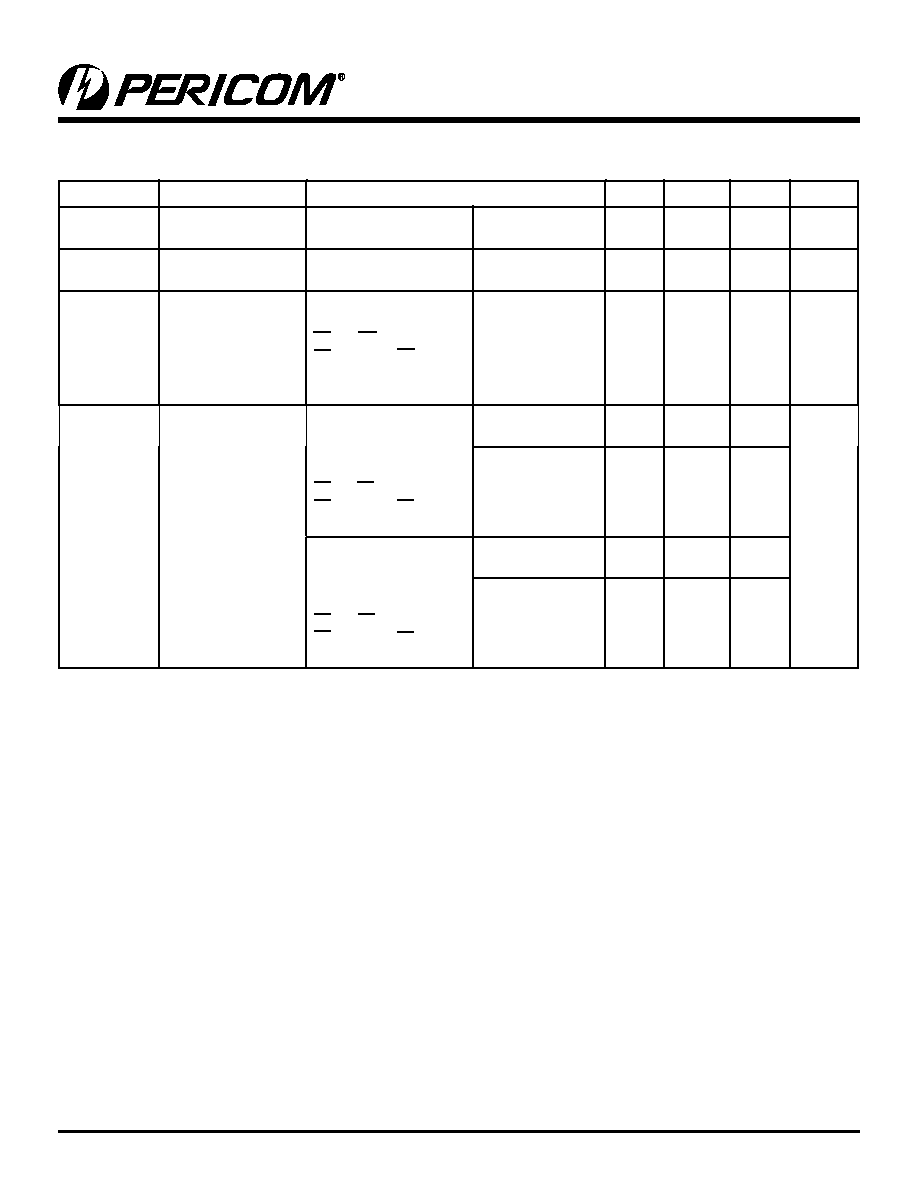
PI74FCT244/2244T Switching Characteristics over Operating Range
Param-
eters
Description
Condi-
tions
(1)
244T/2244T
244AT/2244AT
244CT/2244CT
244DT
Units
Com.
Com.
Com.
Com.
Min
Max
Min
Max
Min
Max
Min
Max
t
PLH
t
PHL
Propagation Delay
C
L
= 50pF
1.5
6.5
1.5
4.8
1.5
4.1
1.5
3.6
ns
t
PZH
t
PZL
Output Enable Time
OE
X
to O
N
1.5
8.0
1.5
6.2
1.5
5.8
1.5
4.8
ns
t
PHZ
t
PLZ
Output Disable
Time
(3)
OE
X
to O
N
1.5
7.0
1.5
5.6
1.5
5.2
1.5
4.0
ns
Notes:
1. See test circuit and wave forms.
2. Minimum limits are guaranteed but not tested on Propagation Delays.
3. This parameter is guaranteed but not production tested.
PI74FCT541/2541T Switching Characteristics over Operating Range
Parameters
Description
Conditions
(1)
541T/2541T
541AT/
2541AT
541CT/
2541CT
541DT
Units
Com.
Com.
Com.
Com.
Min
Max
Min
Max
Min
Max
Min Max
t
PLH
t
PHL
Propagation Delay
D
N
to O
N
C
L
= 50pF
R
L
= 500
1.5
6.0
1.5
4.8
1.5
4.1
1.5
3.8
ns
t
PZH
t
PZL
Output Enable Time
OE
X
to O
N
1.5
9.5
1.5
6.2
1.5
5.8
1.5
5.2
ns
t
PHZ
t
PLZ
Output Disable
Time
(3)
OE
X
to O
N
1.5
6.5
1.5
5.6
1.5
5.2
1.5
5.2
ns
Notes:
1. See test circuit and wave forms.
2. Minimum limits are guaranteed but not tested on Propagation Delays.
3. This parameter is guaranteed but not production tested.
6
PS2011D 09/22/04
PI74FCT244T/2244T
PI74FCT541T/2541T
Octal Buffer/Line Drivers
Ordering Information: PI74FCT244T
Ordering Code
Package Code
Speed Grade
Package Description
PI74FCT244TH
H
Blank
20-pin 209-mil wide plastic SSOP
PI74FCT244TL
L
Blank
20-pin 173-mil wide plastic TSSOP
PI74FCT244TLE
L
Blank
Pb-free & Green, 20-pin 173-mil wide plastic TSSOP
PI74FCT244TQ
Q
Blank
20-pin 150-mil wide plastic QSOP
PI74FCT244TS
S
Blank
20-pin 300-mil wide plastic SOIC
PI74FCT244ATH
H
A
20-pin 209-mil wide plastic SSOP
PI74FCT244ATL
L
A
20-pin 173-mil wide plastic TSSOP
PI74FCT244ATQ
Q
A
20-pin 150-mil wide plastic QSOP
PI74FCT244ATS
S
A
20-pin 300-mil wide plastic SOIC
PI74FCT244ATSE
S
A
Pb-free & Green, 20-pin 300-mil wide plastic SOIC
PI74FCT244CTH
H
C
20-pin 209-mil wide plastic SSOP
PI74FCT244CTL
L
C
20-pin 173-mil wide plastic TSSOP
PI74FCT244CTQ
Q
C
20-pin 150-mil wide plastic QSOP
PI74FCT244CTS
S
C
20-pin 300-mil wide plastic SOIC
PI74FCT244DTQ
Q
D
20-pin 150-mil wide plastic QSOP
PI74FCT244DTS
S
D
20-pin 300-mil wide plastic SOIC
PI74FCT244DTSE
S
D
Pb-free & Green, 20-pin 300-mil wide plastic SOIC
Ordering Information: PI74FCT2244T
Ordering Code
Package Code
Speed Grade
Package Description
PI74FCT2244TQ
Q
Blank
20-pin 150 mil wide plastic QSOP
PI74FCT2244TS
S
Blank
20-pin 300 mil wide plastic SOIC
PI74FCT2244ATH
H
A
20-pin 209 mil wide plastic SSOP
PI74FCT2244ATL
L
A
20-pin 173 mil wide plastic TSSOP
PI74FCT2244ATQ
Q
A
20-pin 150 mil wide plastic QSOP
PI74FCT2244ATS
S
A
20-pin 300 mil wide plastic SOIC
PI74FCT2244CTL
L
C
20-pin 173 mil wide plastic TSSOP
PI74FCT2244CTQ
Q
C
20-pin 150 mil wide plastic QSOP
PI74FCT2244CTS
S
C
20-pin 300 mil wide plastic SOIC
7
PS2011D 09/22/04
PI74FCT244T/2244T
PI74FCT541T/2541T
Octal Buffer/Line Drivers
Pericom Semiconductor Corporation ∑ 1-800-435-2336 ∑ www.pericom.com
Ordering Information: PI74FCT2541T
Ordering Code
Package Code
Speed Grade
Package Description
PI74FCT2541TL
L
Blank
20-pin 173 mil wide plastic TSSOP
PI74FCT2541TQ
Q
Blank
20-pin 150 mil wide plastic QSOP
PI74FCT2541TS
S
Blank
20-pin 300 mil wide plastic SOIC
PI74FCT2541ATH
H
A
20-pin 209 mil wide plastic SSOP
PI74FCT2541ATL
L
A
20-pin 173 mil wide plastic TSSOP
PI74FCT2541ATQ
Q
A
20-pin 150 mil wide plastic QSOP
PI74FCT2541ATS
S
A
20-pin 300 mil wide plastic SOIC
PI74FCT2541CTH
H
C
20-pin 209 mil wide plastic SSOP
PI74FCT2541CTL
L
V
20-pin 173 mil wide plastic TSSOP
Notes:
1. Thermal characteristics can be found on the company web site at www.pericom.com/packaging/
Ordering Information: PI74FCT541T
Ordering Code
Package Code
Speed Grade
Package Description
PI74FCT541TQ
Q
Blank
20-pin 150-mil wide plastic QSOP
PI74FCT541TQE
Q
Blank
Pb-free & Green, 20-pin 150-mil wide plastic QSOP
PI74FCT541TS
S
Blank
20-pin 300-mil wide plastic SOIC
PI74FCT541ATL
L
A
20-pin 173-mil wide plastic TSSOP
PI74FCT541ATQ
Q
A
20-pin 150-mil wide plastic QSOP
PI74FCT541ATS
S
A
20-pin 300-mil wide plastic SOIC
PI74FCT541ATSE
S
A
Pb-free & Green, 20-pin 300-mil wide plastic SOIC
PI74FCT541ATH
H
A
20-pin 209-mil wide plastic SSOP
PI74FCT541CTL
L
C
20-pin 173-mil wide plastic TSSOP
PI74FCT541CTQ
Q
C
20-pin 150-mil wide plastic QSOP
PI74FCT541CTS
S
C
20-pin 300-mil wide plastic SOIC
PI74FCT541CTH
H
C
20-pin 209-mil wide plastic SSOP