1
PS2010A 03/09/96
12345678901234567890123456789012123456789012345678901234567890121234567890123456789012345678901212345678901234567890123456789012123456789012
PI74FCT157T/257T
(25
Series)PI74FCT2157T/2257T
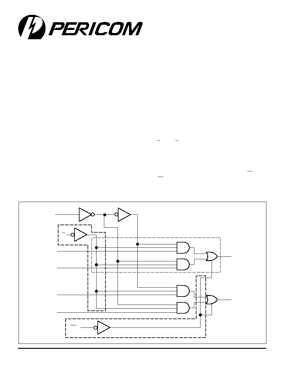
QUAD 2-INPUT MULTIPLEXER
Product Description:
Pericom Semiconductor's PI74FCT series of logic circuits are pro-
duced in the Company's advanced 0.8 micron CMOS technology,
achieving industry leading speed grades. All PI74FCT2XXX devices
have a built-in 25-ohm series resistor on all outputs to reduce noise
because of reflections, thus eliminating the need for an external
terminating resistor.
The PI74FCT157T/257T and PI74FCT2157T/2257T are high-
speed quad 2-input multiplexers. The common select input can be
used to select four bits of data from two sources. The four buffered
outputs present the selected data in the true (non-inverting) form.
The PI74FCT157T/2157T has a common, active-LOW, Enable
input (E). When E is inactive, all four outputs are held LOW. The
PI74FCT157T/2157T can generate any four of the 16 different
funtions of two variables with one common variable. The
PI74FCT157T/2157T can be used as a function generator or to
move data from two different groups of registers to a common bus.
The PI74FCT257/2257T has a common Output Enable (OE) input.
When OE is HIGH, all outputs are switched to a high-impedance
state allowing the outputs to interface directly with bus-oriented
systems.
Logic Block Diagram
12345678901234567890123456789012123456789012345678901234567890121234567890123456789012345678901212345678901234567890123456789012123456789012
12345678901234567890123456789012123456789012345678901234567890121234567890123456789012345678901212345678901234567890123456789012123456789012
PI74FCT157T/257T
(25
Series)PI74FCT2157T/2257T
Fast CMOS
Quad 2-Input Multiplexer
Product Features:
∑ PI74FCT157/257/2157/2257T is pin compatible with bipolar
FASTTM Series at a higher speed and lower power
consumption
∑ 25
series resistor on all outputs (FCT2XXX only)
∑ TTL input and output levels
∑ Low ground bounce outputs (25
series only)
∑ Extremely low static power
∑ Hysteresis on all inputs
∑ Industrial operating temperature range: ≠40∞C to +85∞C
∑ Packages available:
≠ 16-pin 150 mil wide plastic QSOP (Q)
≠ 16-pin 300 mil wide plastic SOIC (S)
≠ 16-pin 150 mil wide plastic SOIC (W)
157
ONLY
S
I
1
B-I
1
D
I
0
B-I
0
D
E
I
1
A
I
0
A
257
ONLY
OE
Z
B
-Z
D
Z
A
3 OTHER MULTIPLEXERS
2
PS2010A 03/09/96
12345678901234567890123456789012123456789012345678901234567890121234567890123456789012345678901212345678901234567890123456789012123456789012
PI74FCT157T/257T
(25
Series)PI74FCT2157T/2257T
QUAD 2-INPUT MULTIPLEXER
PI74FCT157/2157T Product Pin Configuration
PI74FCT257/2257T Product Pin Configuration
Inputs
Outputs Z
N
E/OE
S
I
0
I
1
157/2157 257/2257
H
X
X
X
L
Z
L
H
X
L
L
L
L
H
X
H
H
H
L
L
L
X
L
L
L
L
H
X
H
H
Truth Table
(1)
NOTE:
1.
H = High Voltage Level
X = Don't Care
L = Low Voltage Level
Z = High Impedance
Product Pin Description
Pin Name
Description
I
0
A-I
0
D
Source 0 Data Inputs
I
1
A-I
1
D
Source 1 Data Inputs
E
Enable Input (Active LOW) FCT157/2157
OE
Output Enable (Active LOW) FCT257/2257
S
Select Input
Z
A
-Z
D
Outputs
GND
Ground
V
CC
Power
1
2
3
4
5
6
7
8
16
15
14
13
12
11
10
9
S
I
0
A
I
1
A
Z
A
I
0
B
I
1
B
Z
B
GND
Vcc
E
I
0
C
I
1
C
Z
C
I
0
D
I
1
D
Z
D
16-PIN
Q16
S16
W16
1
2
3
4
5
6
7
8
16
15
14
13
12
11
10
9
S
I
0
A
I
1
A
Z
A
I
0
B
I
1
B
Z
B
GND
Vcc
OE
I
0
C
I
1
C
Z
C
I
0
D
I
1
D
Z
D
16-PIN
Q16
S16
W16
3
PS2010A 03/09/96
12345678901234567890123456789012123456789012345678901234567890121234567890123456789012345678901212345678901234567890123456789012123456789012
PI74FCT157T/257T
(25
Series)PI74FCT2157T/2257T
QUAD 2-INPUT MULTIPLEXER
Maximum Ratings
(Above which the useful life may be impaired. For user guidelines, not tested.)
Storage Temperature ................................................................. ≠65∞C to +150∞C
Ambient Temperature with Power Applied ................................. -40∞C to +85∞C
Supply Voltage to Ground Potential (Inputs & Vcc Only) .......... ≠0.5V to +7.0V
Supply Voltage to Ground Potential (Outputs & D/O Only) ....... ≠0.5V to +7.0V
DC Input Voltage ......................................................................... ≠0.5V to +7.0V
DC Output Current ................................................................................... 120 mA
Power Dissipation ......................................................................................... 0.5W
Note:
Stresses greater than those listed under
MAXIMUM RATINGS may cause permanent
damage to the device. This is a stress rating
only and functional operation of the device at
these or any other conditions above those
indicated in the operational sections of this
specification is not implied. Exposure to
absolute maximum rating conditions for
extended periods may affect reliability.
DC Electrical Characteristics
(Over the Operating Range, T
A
= ≠40∞C to +85∞C, V
CC
= 5.0V ± 5%)
Parameters
Description
Test Conditions
(1)
Min.
Typ
(2)
Max.
Units
V
OH
Output HIGH Voltage
V
CC
= Min., V
IN
= V
IH
or V
IL
I
OH
= ≠15.0 mA
2.4
3.0
V
V
OL
Output LOW Current
V
CC
= Min., V
IN
= V
IH
or V
IL
I
OL
= 48 mA
0.3
0.50
V
V
OL
Output LOW Current
V
CC
= Min., V
IN
= V
IH
or V
IL
I
OL
= 12 mA (25
Series)
0.3
0.50
V
V
IH
Input HIGH Voltage
Guaranteed Logic HIGH Level
2.0
V
V
IL
Input LOW Voltage
Guaranteed Logic LOW Level
0.8
V
I
IH
Input HIGH Current
V
CC
= Max.
V
IN
= V
CC
1
µA
I
IL
Input LOW Current
V
CC
= Max.
V
IN
= GND
≠1
µA
I
OZH
High Impedance
V
CC
= M
AX
.
V
OUT
= 2.7V
1
µA
I
OZL
Output Current
V
OUT
= 0.5V
≠1
µA
V
IK
Clamp Diode Voltage
V
CC
= Min., I
IN
= ≠18 mA
≠0.7
≠1.2
V
I
OFF
Power Down Disable
V
CC
= GND, V
OUT
= 4.5V
--
--
100
µA
I
OS
Short Circuit Current
V
CC
= Max.
(3)
, V
OUT
= GND
≠60
≠120
mA
V
H
Input Hysteresis
200
mV
Capacitance
(T
A
= 25∞C, f = 1 MHz)
Parameters
(4)
Description
Test Conditions
Typ
Max.
Units
C
IN
Input Capacitance
V
IN
= 0V
6
10
pF
C
OUT
Output Capacitance
V
OUT
= 0V
8
12
pF
Notes:
1. For Max. or Min. conditions, use appropriate value specified under Electrical Characteristics for the applicable device type.
2. Typical values are at Vcc = 5.0V, +25∞C ambient and maximum loading.
3. Not more than one output should be shorted at one time. Duration of the test should not exceed one second.
4. This parameter is determined by device characterization but is not production tested.
4
PS2010A 03/09/96
12345678901234567890123456789012123456789012345678901234567890121234567890123456789012345678901212345678901234567890123456789012123456789012
PI74FCT157T/257T
(25
Series)PI74FCT2157T/2257T
QUAD 2-INPUT MULTIPLEXER
Notes:
1. For conditions shown as Max. or Min., use appropriate value specified under Electrical Characteristics for the applicable device.
2. Typical values are at Vcc = 5.0V, +25∞C ambient.
3. Per TTL driven input (V
IN
= 3.4V); all other inputs at Vcc or GND.
4. This parameter is not directly testable, but is derived for use in Total Power Supply Calculations.
5. Values for these conditions are examples of the Icc formula. These limits are guaranteed but not tested.
6. I
C
=I
QUIESCENT
+ I
INPUTS
+ I
DYNAMIC
I
C
= I
CC
+
I
CC
D
H
N
T
+ I
CCD
(f
CP
/2 + f
I
N
I
)
I
CC
= Quiescent Current
I
CC
= Power Supply Current for a TTL High Input (V
IN
= 3.4V)
D
H
= Duty Cycle for TTL Inputs High
N
T
= Number of TTL Inputs at D
H
I
CCD
= Dynamic Current Caused by an Input Transition Pair (HLH or LHL)
f
CP
= Clock Frequency for Register Devices (Zero for Non-Register Devices)
f
I
= Input Frequency
N
I
= Number of Inputs at f
I
All currents are in milliamps and all frequencies are in megahertz.
Power Supply Characteristics
Parameters Description
Test Conditions
(1)
Min.
Typ
(2)
Max.
Units
I
CC
Quiescent Power
V
CC
= Max.
V
IN
= GND or V
CC
0.1
500
µA
Supply Current
I
CC
Supply Current per
V
CC
= Max.
V
IN
= 3.4V
(3)
0.5
2.5
mA
Input @ TTL HIGH
I
CCD
Supply Current per
V
CC
= Max.,
V
IN
= V
CC
0.15
0.25
mA/
Input per MHz
(4)
Outputs Open
V
IN
= GND
MHz
E or OE = GND
One Bit Toggling
50% Duty Cycle
I
C
Total Power Supply
V
CC
= Max.,
V
IN
= V
CC
1.5
3.5
(5)
mA
Current
(6)
Outputs Open
V
IN
= GND
f
I
= 10 MH
Z
50% Duty Cycle
V
IN
= 3.4V
1.8
4.5
(5)
E or OE = GND
V
IN
= GND
One Bit Toggling
V
CC
= Max.,
V
IN
= V
CC
1.5
3.5
(5)
Outputs Open
V
IN
= GND
f
I
= 2.5 MH
Z
50% Duty Cycle
V
IN
= 3.4V
2.5
7.5
(5)
E or OE = GND
V
IN
= GND
Four Bits Toggling
5
PS2010A 03/09/96
12345678901234567890123456789012123456789012345678901234567890121234567890123456789012345678901212345678901234567890123456789012123456789012
PI74FCT157T/257T
(25
Series)PI74FCT2157T/2257T
QUAD 2-INPUT MULTIPLEXER
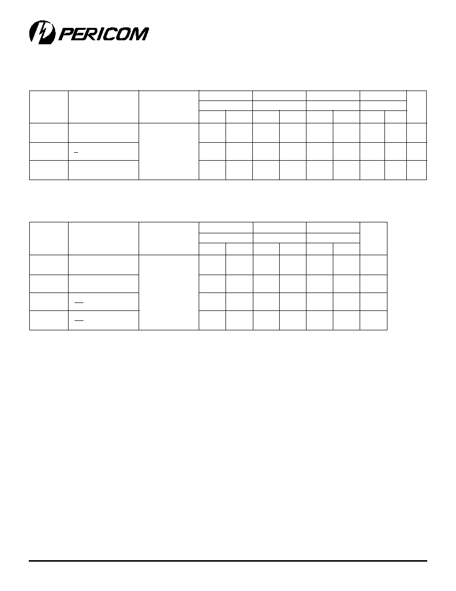
PI74FCT257/2257T Switching Characteristics over Operating Range
257T/2257T
257AT/2257AT 257CT/2257CT
Com.
Com.
Com.
Parameters
Description
Conditions
(1)
Min
Max
Min
Max
Min
Max
Unit
t
PLH
Propagation Delay
C
L
= 50 pF
1.5
6.0
1.5
5.0
1.5
4.3
ns
t
PHL
I
N
to Z
N
R
L
= 500
t
PLH
Propagation Delay
1.5
10.5
1.5
7.0
1.5
5.2
ns
t
PHL
S to Z
N
t
PZH
Output Enable Time
1.5
8.5
1.5
7.0
1.5
6.0
ns
t
PZL
OE to Z
N
t
PZH
Output Disable Time
(3)
1.5
6.0
1.5
5.5
1.5
5.0
ns
t
PZL
OE to Z
N
PI74FCT157/2157T Switching Characteristics over Operating Range
157T/2157T
157AT/2157AT 157CT/2157CT
157DT
Com.
Com.
Com.
Com.
Parameters
Description
Conditions
(1)
Min
Max
Min
Max
Min
Max
Min
Max
Unit
t
PLH
Propagation Delay
C
L
= 50 pF
1.5
6.0
1.5
5.0
1.5
4.3
1.5
3.9
ns
t
PHL
I
N
to Z
N
R
L
= 500
t
PLH
Propagation Delay
1.5
10.5
1.5
6.0
1.5
4.8
1.5
4.4
ns
t
PHL
E to Z
N
t
PLH
Propagation Delay
1.5
10.5
1.5
7.0
1.5
5.2
1.5
4.6
ns
t
PHL
S to Z
N
Notes:
1. See test circuit and wave forms.
2. Minimum limits are guaranteed but not tested on Propagation Delays.
3. This parameter guaranteed but not production tested.
Pericom Semiconductor Corporation
2380 Bering Drive ∑ San Jose, CA 95131 ∑ 1-800-435-2336 ∑ Fax (408) 435-1100 ∑ http://www.pericom.com