1
PS7067E 11/09/98
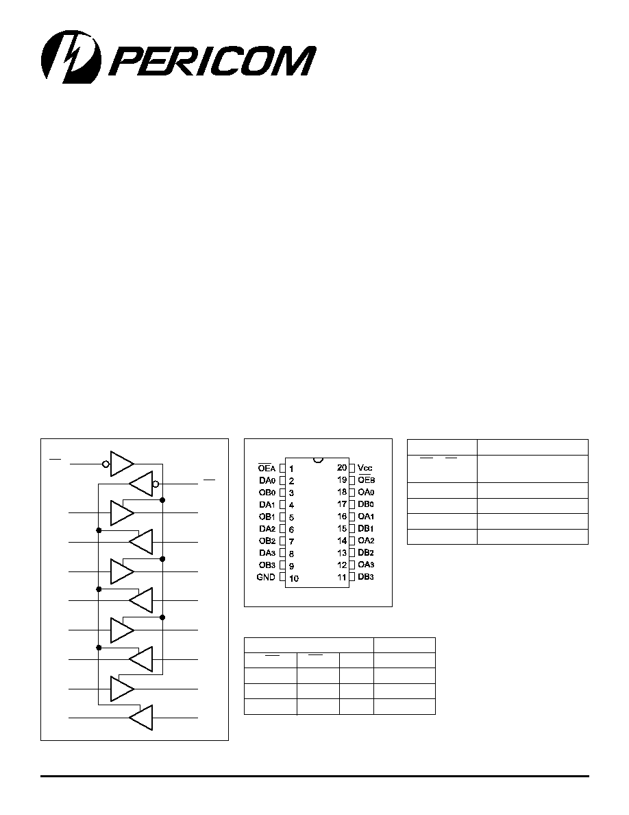
Logic Block Diagram
Pin Configuration
Pin Description
Pin Name
Description
OE
A
, OE
B
3-State Output Enable
Inputs (Active LOW)
Dxx
Inputs
Oxx
Outputs
GND
Ground
V
CC
Power
Inputs
Outputs
OE
A
OE
B
D
XX
O
XX
L
L
L
L
L
L
H
H
H
H
X
Z
Truth Table
(1)
Note:
1. H = High Voltage Level, X = Don't Care,
L = Low Voltage Level, Z = High Impedance
Description
Pericom Semiconductor's PI74FCT3 series of logic circuits are
produced in the Company's advanced 0.6 micron CMOS technology,
achieving industry leading speed grades.
The PI74FCT3244 is an 8-bit buffer/line driver designed for driving
high capacitive memory loads. With its balanced-drive
characteristics, this high-speed, low power device provides lower
ground bounce, transmission line matching of signals, fewer line
reflections and lower EMI and RFI effects. This makes it ideal for
driving on-board buses and transmission lines.
The PI74FCT3244 can be driven from either 3.3V or 5.0V devices
allowing this device to be used as a translator in a mixed
3.3/5.0V system.
Features
∑ Advanced Low Power CMOS operation
∑ Compatible with LVC class of products
∑ Compatible with industry standard octal pinouts
∑ Excellent output drive capability:
Balanced Drives (24mA sink and source)
∑ Can serve as a 5V to 3V translator
∑ Inputs can be driven by 3.3 V or 5V devices
∑ Low ground bounce outputs
∑ Hysteresis on all inputs
∑ Industrial operating temperature range:
≠40∞C to +85∞C
∑ Packages available:
≠ 20-pin 173 mil wide plastic TSSOP (L)
≠ 20-pin 150 mil wide plastic QSOP (Q)
≠ 20-pin 150 mil wide plastic TQSOP (R)
≠ 20-pin 300 mil wide plastic SOIC (S)
OE
A
DA
0
OB
0
OB
1
DA
1
OB
2
DA
2
OB
3
DA
3
OA
0
DB
0
OE
B
OA
1
DB
1
OA
2
DB
2
OA
3
DB
3
20-PIN
L20
Q20
R20
S20
12345678901234567890123456789012123456789012345678901234567890121234567890123456789012345678901212345678901234567890123456789012123456789012
12345678901234567890123456789012123456789012345678901234567890121234567890123456789012345678901212345678901234567890123456789012123456789012
PI74FCT3244
Fast CMOS 3.3V 8-Bit
Buffer/Line Driver
PI74FCT3244
3.3V 8-BIT BUFFER/LINE DRIVER
2
PS7067E 11/09/98
12345678901234567890123456789012123456789012345678901234567890121234567890123456789012345678901212345678901234567890123456789012123456789012
12345678901234567890123456789012123456789012345678901234567890121234567890123456789012345678901212345678901234567890123456789012123456789012
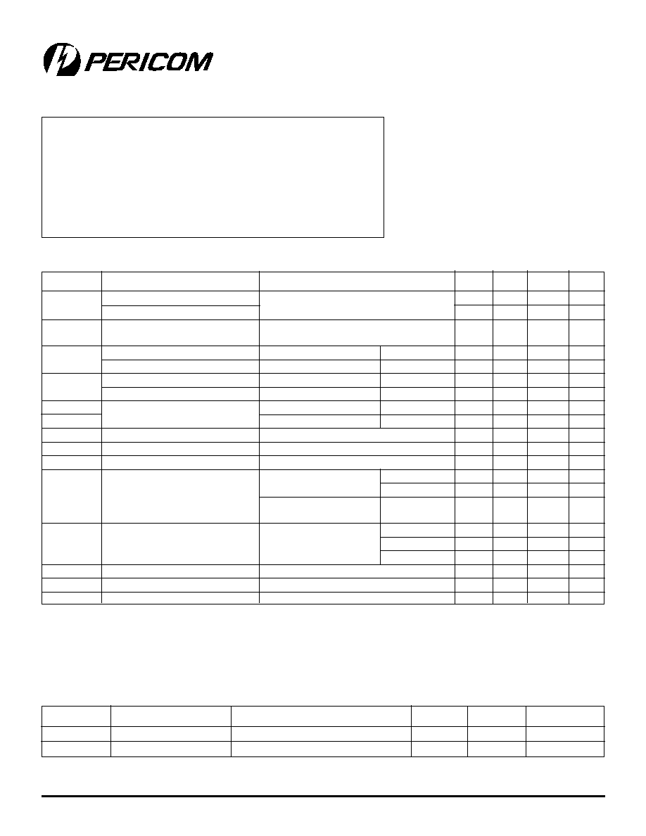
Storage Temperature .............................................................. ≠65∞C to +150∞C
Ambient Temperature with Power Applied ............................. ≠40∞C to +85∞C
Supply Voltage to Ground Potential (Inputs & Vcc Only) ....... ≠0.5V to +7.0V
Supply Voltage to Ground Potential (Outputs & D/O Only) ... ≠0.5V to +7.0V
DC Input Voltage ..................................................................... ≠0.5V to +7.0V
DC Output Current ............................................................................... 120 mA
Power Dissipation ..................................................................................... 1.0W
Note:
Stresses greater than those listed under MAXIMUM
RATINGS may cause permanent damage to the
device. This is a stress rating only and functional
operation of the device at these or any other condi-
tions above those indicated in the operational sec-
tions of this specification is not implied. Exposure to
absolute maximum rating conditions for extended
periods may affect reliability.
DC Electrical Characteristics
(Over the Operating Range, T
A
= ≠40∞C to +85∞C, V
CC
= 2.7V to 3.6V)
Parameters
Description
Test Conditions
(1)
Min.
Typ.
(2)
Max.
Units
V
IH
Input HIGH Voltage (Input pins)
Guaranteed Logic HIGH Level
2.2
--
5.5
V
Input HIGH Voltage (I/O pins)
2.0
--
5.5
V
V
IL
Input LOW Voltage
Guaranteed Logic LOW Level
≠0.5
--
0.8
V
(Input and I/O pins)
I
IH
Input HIGH Current (Input pins)
V
CC
= Max.
V
IN
= 5.5V
--
--
±1
µA
Input HIGH Current (I/O pins)
V
CC
= Max.
V
IN
= V
CC
--
--
±1
µA
I
IL
Input LOW Current (Input pins)
V
CC
= Max.
V
IN
= GND
--
--
±1
µA
Input LOW Current (I/O pins)
V
CC
= Max.
V
IN
= GND
--
--
±1
µA
I
OZH
High Impedance Output Current
V
CC
= Max.
V
OUT
= 5.5V
--
--
±1
µA
I
OZL
(3-State Output pins)
V
CC
= Max.
V
OUT
= GND
--
--
±1
µA
V
IK
Clamp Diode Voltage
V
CC
= Min., I
IN
= ≠18mA
--
≠0.7
≠1.2
V
I
ODH
Output HIGH Current
V
CC
= 3.3V, V
IN
= V
IH
or V
IL
, V
O
= 1.5V
(3)
≠36
≠60
≠110
mA
I
ODL
Output LOW Current
V
CC
= 3.3V, V
IN
= V
IH
or V
IL
, V
O
= 1.5V
(3)
50
90
200
mA
V
OH
Output HIGH Voltage
V
CC
= Min.
I
OH
= ≠0.1mA Vcc-0.2
--
--
V
V
IN
= V
IH
or V
IL
I
OH
= ≠3mA
2.4
3.0
--
V
V
CC
= 3.0V,
I
OH
= ≠8mA
2.4
(5)
3.0
--
V
V
IN
= V
IH
or V
IL
I
OH
= ≠24mA
2.0
--
--
V
OL
Output LOW Voltage
V
CC
= Min.
I
OL
= 0.1mA
--
--
0.2
V
V
IN
= V
IH
or V
IL
I
OL
= 16mA
--
0.2
0.4
V
I
OL
= 24mA
--
0.3
0.5
V
I
OS
Short Circuit Current
(4)
V
CC
= Max.
(3)
, V
OUT
= GND
≠60
≠85
≠240
mA
I
OFF
Power Down Disable
V
CC
= 0V, V
IN
or V
OUT
4.5V
--
--
±100
µA
V
H
Input Hysteresis
--
150
--
mV
Capacitance
(T
A
= 25∞C, f = 1 MHz)
Parameters
(1)
Description
Test Conditions
Typ.
Max.
Units
C
IN
Input Capacitance
V
IN
= 0V
4.5
6
pF
C
OUT
Output Capacitance
V
OUT
= 0V
5.5
8
pF
Notes:
1. For Max. or Min. conditions, use appropriate value specified under Electrical Characteristics for the applicable device type.
2. Typical values are at Vcc = 3.3V, +25∞C ambient and maximum loading.
3. Not more than one output should be shorted at one time. Duration of the test should not exceed one second.
4. This parameter is guaranteed but not tested.
5. V
OH
= V
CC
≠ 0.6V at rated current.
Note:
1. This parameter is determined by device characterization but is not production tested.
Maximum Ratings
(Above which the useful life may be impaired. For user guidelines, not tested.)
PI74FCT3244
3.3V 8-BIT BUFFER/LINE DRIVER
3
PS7067E 11/09/98
12345678901234567890123456789012123456789012345678901234567890121234567890123456789012345678901212345678901234567890123456789012123456789012
12345678901234567890123456789012123456789012345678901234567890121234567890123456789012345678901212345678901234567890123456789012123456789012
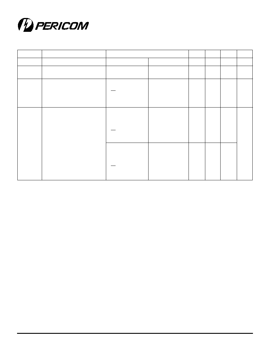
Power Supply Characteristics
Parameters Description
Test Conditions
(1)
Min.
Typ.
(2)
Max.
Units
I
CC
Quiescent Power Supply Current
V
CC
= Max.
V
IN
= GND or V
CC
0.1
10
µA
I
CC
Quiescent Power Supply Current
V
CC
= Max.
V
IN
= V
CC
≠ 0.6V
(3)
2.0
30
µA
TTL Inputs HIGH
I
CCD
Dynamic Power Supply
(4)
V
CC
= Max.,
V
IN
= V
CC
95
100
µA/
Outputs Open
V
IN
= GND
MHz
OE
X
= GND
One Bit Toggling
50% Duty Cycle
I
C
Total Power Supply
V
CC
= Max.,
V
IN
= V
CC
≠ 0.6V
0.97
2.3
mA
Current
(6)
Outputs Open
V
IN
= GND
f
I
= 10 MH
Z
50% Duty Cycle
OE
X
= GND
One Bit Toggling
V
CC
= Max.,
V
IN
= V
CC
≠ 0.6V
1.9
4.7
(5)
Outputs Open
V
IN
= GND
f
I
= 2.5 MH
Z
50% Duty Cycle
OE
X
= GND
8 Bits Toggling
Notes:
1. For Max. or Min. conditions, use appropriate value specified under Electrical Characteristics for the applicable device.
2. Typical values are at Vcc = 3.3V, +25∞C ambient.
3. Per TTL driven input; all other inputs at Vcc or GND.
4. This parameter is not directly testable, but is derived for use in Total Power Supply Calculations.
5. Values for these conditions are examples of the Icc formula. These limits are guaranteed but not tested.
6. I
C
=I
QUIESCENT
+ I
INPUTS
+ I
DYNAMIC
I
C
= I
CC
+
I
CC
D
H
N
T
+ I
CCD
(f
CP
/2 + f
I
N
I
)
I
CC
= Quiescent Current (I
CCL
, I
CCH
and I
CCZ
)
I
CC
= Power Supply Current for a TTL High Input
D
H
= Duty Cycle for TTL Inputs High
N
T
= Number of TTL Inputs at D
H
I
CCD
= Dynamic Current Caused by an Input Transition Pair (HLH or LHL)
f
CP
= Clock Frequency for Register Devices (Zero for Non-Register Devices)
N
CP
= Number of Clock Inputs at f
CP
f
I
= Input Frequency
N
I
= Number of Inputs at f
I
All currents are in milliamps and all frequencies are in megahertz.

PI74FCT3244
3.3V 8-BIT BUFFER/LINE DRIVER
4
PS7067E 11/09/98
12345678901234567890123456789012123456789012345678901234567890121234567890123456789012345678901212345678901234567890123456789012123456789012
12345678901234567890123456789012123456789012345678901234567890121234567890123456789012345678901212345678901234567890123456789012123456789012
Notes:
1. Propagation Delays and Enable/Disable times are with V
CC
= 3.3V ± 0.3V, normal range.
For V
CC
= 2.7V, extended range, all Propagation Delays and Enable/Disable times should
be degraded by 20%.
2. See test circuit and wave forms.
3. Minimum limits are guaranteed but not tested on Propagation Delays.
4. This parameter is guaranteed but not production tested.
5. Skew between any two outputs, of the same package, switching in the same direction.
This parameter is guaranteed by design.
Switching Characteristics over Operating Range
(1)
FCT3244
Com.
Parameters
Description
Conditions
(2)
Min.
(3)
Max.
Units
t
PLH
Propagation Delay
C
L
= 50pF
1.5
4.1
t
PHL
D
XX
to O
XX
R
L
= 500
t
PZH
Output Enable Time
1.5
5.8
ns
t
PZL
OEx to Oxx
t
PHZ
Output Disable Time
(4)
1.5
5.2
t
PLZ
OEx to Oxx
t
SK
(o)
Output Skew
(5)
0.5
Pericom Semiconductor Corporation
2380 Bering Drive ∑ San Jose, CA 95131 ∑ 1-800-435-2336 ∑ Fax (408) 435-1100 ∑ http://www.pericom.com