PI74FCT521T
8-Bit Identity Comparator
1
PS2019B 07/02/02
12345678901234567890123456789012123456789012345678901234567890121234567890123456789012345678901212345678901234567890123456789012123456789012
Fast CMOS
8-Bit Identity Comparator
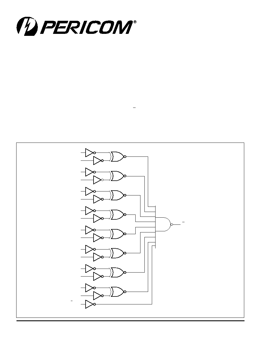
Logic Block Diagram
12345678901234567890123456789012123456789012345678901234567890121234567890123456789012345678901212345678901234567890123456789012123456789012
12345678901234567890123456789012123456789012345678901234567890121234567890123456789012345678901212345678901234567890123456789012123456789012
PI74FCT521T
Product Description
Pericom Semiconductors PI74FCT series of logic circuits are pro-
duced in the Companys advanced 0.8 micron CMOS technology,
achieving industry leading speed grades.
The PI74FCT521T is an 8-bit identity comparator. When two words
of up to eight bits are compared, a bit-for-bit match of the two words
provides a LOW output. The comparison can be extended over
multiple words by the expansion input. The expansion input I
A
=
B
also serves as an active LOW enable input.
Product Features
PI74FCT521T is pin compatible with bipolar FAST Series at
a higher speed and lower power consumption
TTL input and output levels
Extremely low static power
Hysteresis on all inputs
Industrial operating temperature range: 40�C to +85�C
Packages available:
20-pin 209 mil wide plastic SSOP (H)
20-pin 173 mil wide plastic TSSOP (L)
20-pin 300 mil wide plastic DIP (P)
20-pin 150 mil wide plastic QSOP (Q)
20-pin 150 mil wide plastic TQSOP (R)
20-pin 300 mil wide plastic SOIC (S)
B
0
O
A=B
A
0
B
1
A
1
B
2
A
2
B
3
A
3
B
4
A
4
B
5
A
5
B
6
A
6
B
7
A
7
I
A=B
PI74FCT521T
8-Bit Identity Comparator
2
PS2019B 07/02/02
12345678901234567890123456789012123456789012345678901234567890121234567890123456789012345678901212345678901234567890123456789012123456789012
1
2
3
4
5
6
7
8
9
10
20
19
18
17
16
15
14
13
12
11
I
A=B
A
0
B
0
A
1
B
1
A
2
B
2
A
3
B
3
GND
Vcc
O
A=B
B
7
A
7
B
6
A
6
B
5
A
5
B
4
A
4
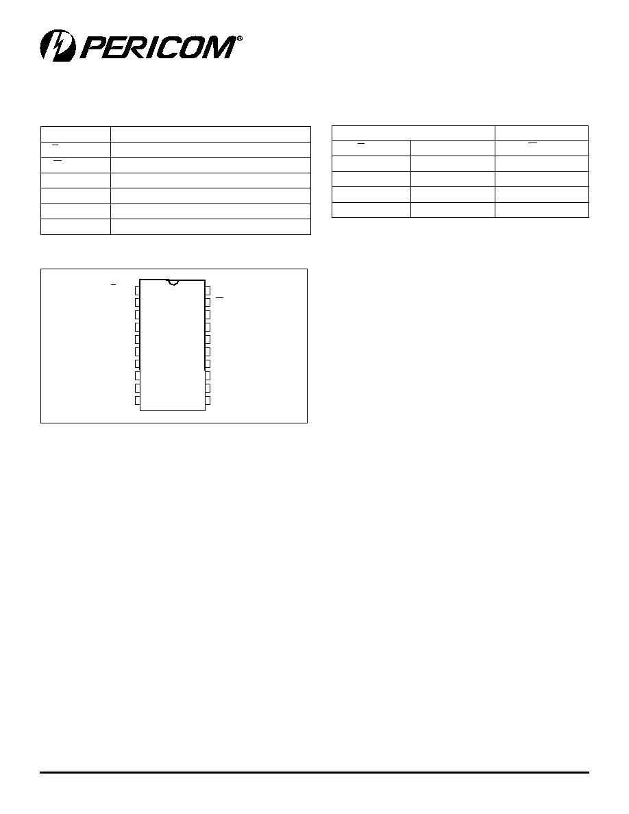
Inputs
Output
I
A=B
A, B
O
A=B
L
A = B*
L
L
A
B
H
H
A = B*
H
H
A
B
H
Truth Table
(1)
NOTE: 1.H = High Voltage Level
L = Low Voltage Level,
*A
0
= B
0
, A
1
= B
1
, A
2
= B
2
, etc.
Product Pin Description
Pin Name
Description
I
A=B
Expansion or Enable Input (Active LOW)
O
A=B
Identity Output (Active LOW)
A
0
A
7
Word A Inputs
B
0
B
7
Word B Inputs
GND
Ground
V
CC
Power
Product Pin Configuration
20-Pin
L,P,Q,
R,S,H

PI74FCT521T
8-Bit Identity Comparator
3
PS2019B 07/02/02
12345678901234567890123456789012123456789012345678901234567890121234567890123456789012345678901212345678901234567890123456789012123456789012
Maximum Ratings
(Above which the useful life may be impaired. For user guidelines, not tested.)
Storage Temperature .................................................................... 65�C to +150�C
Ambient Temperature with Power Applied .....................................-40�C to +85�C
Supply Voltage to Ground Potential (Inputs & Vcc Only) .............. 0.5V to +7.0V
Supply Voltage to Ground Potential (Outputs & D/O Only) ........... 0.5V to +7.0V
DC Input Voltage ............................................................................ 0.5V to +7.0V
DC Output Current ..................................................................................... 120 mA
Power Dissipation ..........................................................................................0.5W
Note:
Stresses greater than those listed under
MAXIMUM RATINGS may cause permanent
damage to the device. This is a stress rating
only and functional operation of the device at
these or any other conditions above those
indicated in the operational sections of this
specification is not implied. Exposure to
absolute maximum rating conditions for
extended periods may affect reliability.
DC Electrical Characteristics
(Over the Operating Range, T
A
= 40�C to +85�C, V
CC
= 5V � 5%)
Parameters Description
Test Conditions
(1)
Min.
Typ
(2)
Max.
Units
V
OH
Output HIGH Voltage
V
CC
= Min., V
IN
= V
IH
or V
IL
I
OH
= 15.0 mA
2.4
3.0
V
V
OL
Output LOW Current
V
CC
= Min., V
IN
= V
IH
or V
IL
I
OL
= 48 mA
0.3
0.50
V
V
IH
Input HIGH Voltage
Guaranteed Logic HIGH Level
2.0
V
V
IL
Input LOW Voltage
Guaranteed Logic LOW Level
0.8
V
I
IH
Input HIGH Current
V
CC
= Max.V
IN
= V
CC
1
�A
I
IL
Input LOW Current
V
CC
= Max.V
IN
= GND
1
�A
V
IK
Clamp Diode Voltage
V
CC
= Min., I
IN
= 18 mA
0.7
1.2
V
I
OS
Short Circuit Current
V
CC
= Max.
(3)
, V
OUT
= GND
60
120
mA
I
OFF
Power Down Disable
V
CC
= GND, V
OUT
= 4.5V
100
�A
V
H
Input Hysteresis
200
mV
Capacitance
(T
A
= 25�C, f = 1 MHz)
Parameters
(4)
Description
Test Conditions
Typ
Max.
Units
C
IN
Input Capacitance
V
IN
= 0V
6
10
pF
C
OUT
Output Capacitance
V
OUT
= 0V
8
12
pF
Notes:
1. For Max. or Min. conditions, use appropriate value specified under Electrical Characteristics for the applicable device type.
2.Typical values are at Vcc = 5.0V, +25�C ambient and maximum loading.
3.Not more than one output should be shorted at one time. Duration of the test should not exceed one second.
4.This parameter is determined by device characterization but is not production tested.

PI74FCT521T
8-Bit Identity Comparator
4
PS2019B 07/02/02
12345678901234567890123456789012123456789012345678901234567890121234567890123456789012345678901212345678901234567890123456789012123456789012
Switching Characteristics over Operating Range
521T
521AT
521BT
521CT
521DT
Com.
Com.
Com.
Com.
Com.
Parameters
Description
Conditions
(1)
Min
Max
Min
Max
Min
Max
Min
Max
Min
Max Unit
t
PLH
Propagation Delay
C
L
= 50 pF
1.5
10.0
1.5
7.2
1.5
5.5
1.5
4.5
1.5
4.2
ns
t
PHL
A
N
or B
N
to O
A
=
B
R
L
= 500
t
PLH
Propagation Delay
1.5
9.0
1.5
6.0
1.5
4.6
1.5
4.1
1.5
3.8
ns
t
PHL
I
A
=
B
to O
A
=
B
Power Supply Characteristics
Parameters Description
Test Conditions
(1)
Min.
Typ
(2)
Max.
Units
I
CC
Quiescent Power
V
CC
= Max.V
IN
= GND or V
CC
0.1
500
�A
Supply Current
I
CC
Supply Current per
V
CC
= Max.V
IN
= 3.4V
(3)
0.5
2.0
mA
Input @ TTL HIGH
I
CCD
Supply Current per
V
CC
= Max.,
V
IN
= V
CC
0.15
0.25
mA/
Input per MHz
(4)
Outputs Open
V
IN
= GND
MHz
One Input Toggling
50% Duty Cycle
I
C
Total Power Supply
V
CC
= Max.,
V
IN
= V
CC
1.5
3.5
(5)
mA
Current
(6)
Outputs Open
V
IN
= GND
f
I
= 10 MH
Z
V
IN
= 3.4V
1.8
4.5
(5)
50% Duty Cycle
V
IN
= GND
One Bit Toggling
Notes:
1. For conditions shown as Max. or Min., use appropriate value specified under Electrical Characteristics for the applicable device.
2.Typical values are at Vcc = 5.0V, +25�C ambient.
3.Per TTL driven input (V
IN
= 3.4V); all other inputs at Vcc or GND.
4.This parameter is not directly testable, but is derived for use in Total Power Supply Calculations.
5.Values for these conditions are examples of the Icc formula. These limits are guaranteed but not tested.
6.I
C
=I
QUIESCENT
+ I
INPUTS
+ I
DYNAMIC
I
C
= I
CC
+
I
CC
D
H
N
T
+ I
CCD
(f
CP
/2 + f
I
N
I
)
I
CC
= Quiescent Current
I
CC
= Power Supply Current for a TTL High Input (V
IN
= 3.4V)
D
H
= Duty Cycle for TTL Inputs High
N
T
= Number of TTL Inputs at D
H
I
CCD
= Dynamic Current Caused by an Input Transition Pair (HLH or LHL)
f
CP
= Clock Frequency for Register Devices (Zero for Non-Register Devices)
f
I
= Input Frequency
N
I
= Number of Inputs at f
I
All currents are in milliamps and all frequencies are in megahertz.
Notes:
1.See Test Circuit and Waveforms
2.Minimum limits are guaranteed but not tested on Propagation Delays.
PI74FCT521T
8-Bit Identity Comparator
5
PS2019B 07/02/02
12345678901234567890123456789012123456789012345678901234567890121234567890123456789012345678901212345678901234567890123456789012123456789012
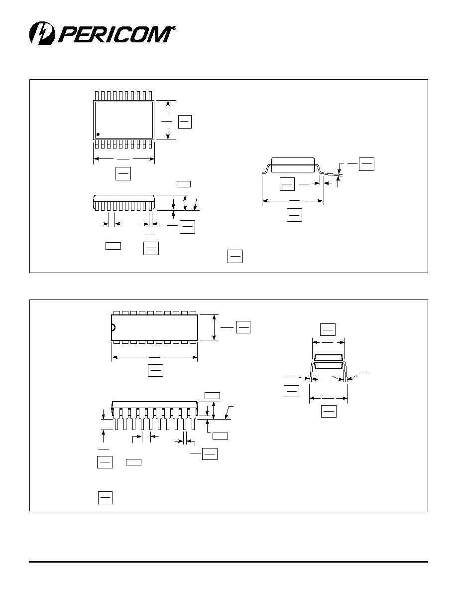
.252
.260
.047
1.20
.002
.006
SEATING
PLANE
.0256
BSC
.018
.030
.004
.008
.238
.269
1
20
.169
.177
X.XX
X.XX
DENOTES CONTROLLING
DIMENSIONS IN MILLIMETERS
0.05
0.15
6.1
6.7
0.45
0.75
0.09
0.20
4.3
4.5
6.4
6.6
0.65
0.19
0.30
.007
.012
Max
0.015
.210
Max.
.980
1.060
1
.115
.150
.100
typical
.014
.022
20
SEATING PLANE
.008
.014
.300
.325
0�
15�
.240
.280
.310
.380
X.XX
X.XX
DENOTES DIMENSIONS
IN MILLIMETERS
24.9
26.9
6.09
7.11
7.62
8.25
7.87
9.65
0.20
0.35
5.33
2.921
3.81
2.54
0.42
0.51
0.381
Min.
20-pin 173 mil wide plastic TSSOP (L) Package
20-pin 300 mil wide plastic DIP (P)

PI74FCT521T
8-Bit Identity Comparator
6
PS2019B 07/02/02
12345678901234567890123456789012123456789012345678901234567890121234567890123456789012345678901212345678901234567890123456789012123456789012
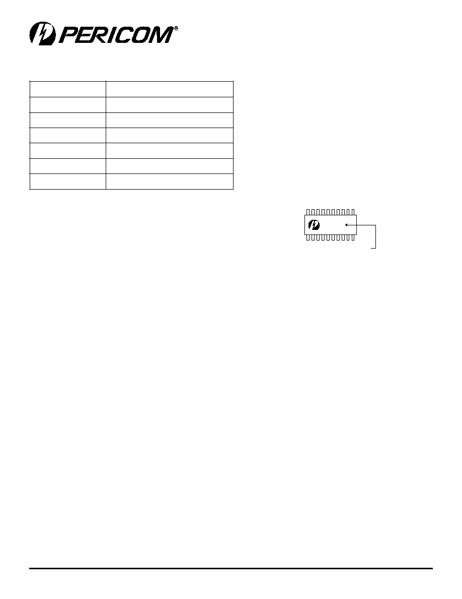
.189
.197
.053
.069
.004
.010
SEATING
PLANE
.025
BSC
.007
.010
.228
.244
1
16
.150
.157
.016
.050
X.XX
X.XX
DENOTES DIMENSIONS IN MILLIMETERS
0.635
4.80
5.00
1.35
1.75
5.79
6.19
0.101
0.254
.008
.012
0.203
0.305
3.81
3.99
0.178
0.254
0.38
0.41
1.27
.008
0.203
.015 x 45
�
REF
Detail A
Detail A
.008
0.20
MIN.
Guage Plane
.010
0.254
.041
1.04
REF
.016
.035
0.41
0.89
0�-6�
.008
.013
0.20
0.33
.002
.336
.344
.047
Max
.008
.012
SEATING
PLANE
.025
BSC
.016
.050
.0075
.0098
.2284
.2440
1
24
.149
.157
X.XX
X.XX
DENOTES DIMENSIONS
IN MILLIMETERS
5.80
6.20
0.41
1.27
0.19
0.25
3.78
3.99
1.20
0.203
0.305
0.050
8.55
8.75
0.635
Min
20-pin 150 mil wide plastic QSOP (Q) Package
20-pin 150 mil wide plastic TSSOP (R) Package

PI74FCT521T
8-Bit Identity Comparator
7
PS2019B 07/02/02
12345678901234567890123456789012123456789012345678901234567890121234567890123456789012345678901212345678901234567890123456789012123456789012
SEATING
PLANE
.050
BSC
1
20
0-8�
.2914
.2992
X.XX
X.XX
DENOTES CONTROLLING
DIMENSIONS IN MILLIMETERS
7.40
7.60
.496
.511
12.60
12.99
1.27
.0926
.1043
2.35
2.65
.394
.419
10.00
10.65
.0040
.0118
0.10
0.30
.013
.020
0.33
0.51
.010
.029
0.254
0.737
.0091
.0125
0.23
0.32
0.41
1.27
.016
.050
x 45�
.020
.030
0.508
0.762
REF
20-pin 300 mil wide plastic SOIC (S) Package
.272
.295
.078
.002
SEATING
PLANE
.0098
Max.
.0256
BSC
.022
.037
.004
.009
.291
.322
1
20
.197
.220
0.25
X.XX
X.XX
DENOTES DIMENSIONS
IN MILLIMETERS
0.050
7.40
8.20
0.55
0.95
0.09
0.25
5.00
5.60
2.00
6.90
7.50
0.65
Max
Min
20-pin 209 mil wide plastic SSOP (H) Package
PI74FCT521T
8-Bit Identity Comparator
8
PS2019B 07/02/02
12345678901234567890123456789012123456789012345678901234567890121234567890123456789012345678901212345678901234567890123456789012123456789012
Pericom Semiconductor Corporation
2380 Bering Drive San Jose, CA 95131 1-800-435-2336 Fax (408) 435-1100 http://www.pericom.com
Ordering Information
PI74FCT
245TQ A
0010BSC
"A" is the speed code letter identifier
Part Marking Information
Pericom s standard product mark follows our standard part number
ordering information, except for those products with a speed letter
code. For marking purposes, the speed letter code mark is placed
after the package code letter, rather than after the device number as
it is ordered.
Although all products are marked immediately after assembly to
assure material traceability, Pericom does not usually mark the
speed code at that time. After electrical test screening and speed
binning has been completed, we then perform an add mark
operation which places the speed code letter at the end of the
complete part number.
Please refer to the example shown below:
Part Number as ordered: PI74FCT245ATQ
Example of Part Number as marked:
Notes:
1) 8-pin DIP, 8-pin SOIC, 8-pin TSSOP, 14-pin SOIC, 16-pin QSOP,
SC70, MSOP, and SOT23 packages are not marked with the
Pericom logo due to space limitations on the package.
t
r
a
P
e
g
a
k
c
a
P
n
i
P
H
T
1
2
5
T
C
F
4
7
I
P
)
H
(
P
O
S
S
ci
t
s
al
p
e
d
i
w
li
m
9
0
2
n
i
p
-
0
2
L
T
1
2
5
T
C
F
4
7
I
P
)
L
(
P
O
S
S
T
ci
t
s
al
p
e
d
i
w
li
m
3
7
1
n
i
p
-
0
2
P
T
1
2
5
T
C
F
4
7
I
P
)
P
(
P
I
D
P
ci
t
s
al
p
e
d
i
w
li
m
0
0
3
n
i
p
-
0
2
Q
T
1
2
5
T
C
F
4
7
I
P
)
Q
(
P
O
S
Q
ci
t
s
al
p
e
d
i
w
li
m
0
5
1
n
i
p
-
0
2
R
T
1
2
5
T
C
F
4
7
I
P
)
R
(
P
O
S
Q
T
ci
t
s
al
p
e
d
i
w
li
m
0
5
1
n
i
p
-
0
2
S
T
1
2
5
T
C
F
4
7
I
P
)
S
(
C
I
O
S
ci
t
s
al
p
e
d
i
w
li
m
0
0
3
n
i
p
-
0
2