DATASHEET SEARCH SITE | WWW.ALLDATASHEET.COM
1
PS8644A 03/23/04
12345678901234567890123456789012123456789012345678901234567890121234567890123456789012345678901212345678901234567890123456789012123456789012
12345678901234567890123456789012123456789012345678901234567890121234567890123456789012345678901212345678901234567890123456789012123456789012
SOTiny
TM
Gate STX Dual
Schmitt-Trigger Inverter
Features
· High-Speed: t
PD
= 3.2ns typical into 50pF @ 5V V
CC
· Broad Operating Range: V
CC
= 1.65V to 5.5V
· Power down high-impedance inputs/outputs
· High Output Drive: ±24mA at 3V V
CC
· Package: 6-pin space saving SC70 (C)
Description
The PI74STX2G14 is a Dual Schmitt-Trigger inverter that operates
over the 1.65V to 5.5V V
CC
operating range.
Pericom's PI74STX series of products are produced using the
Company's advanced submicron technology.
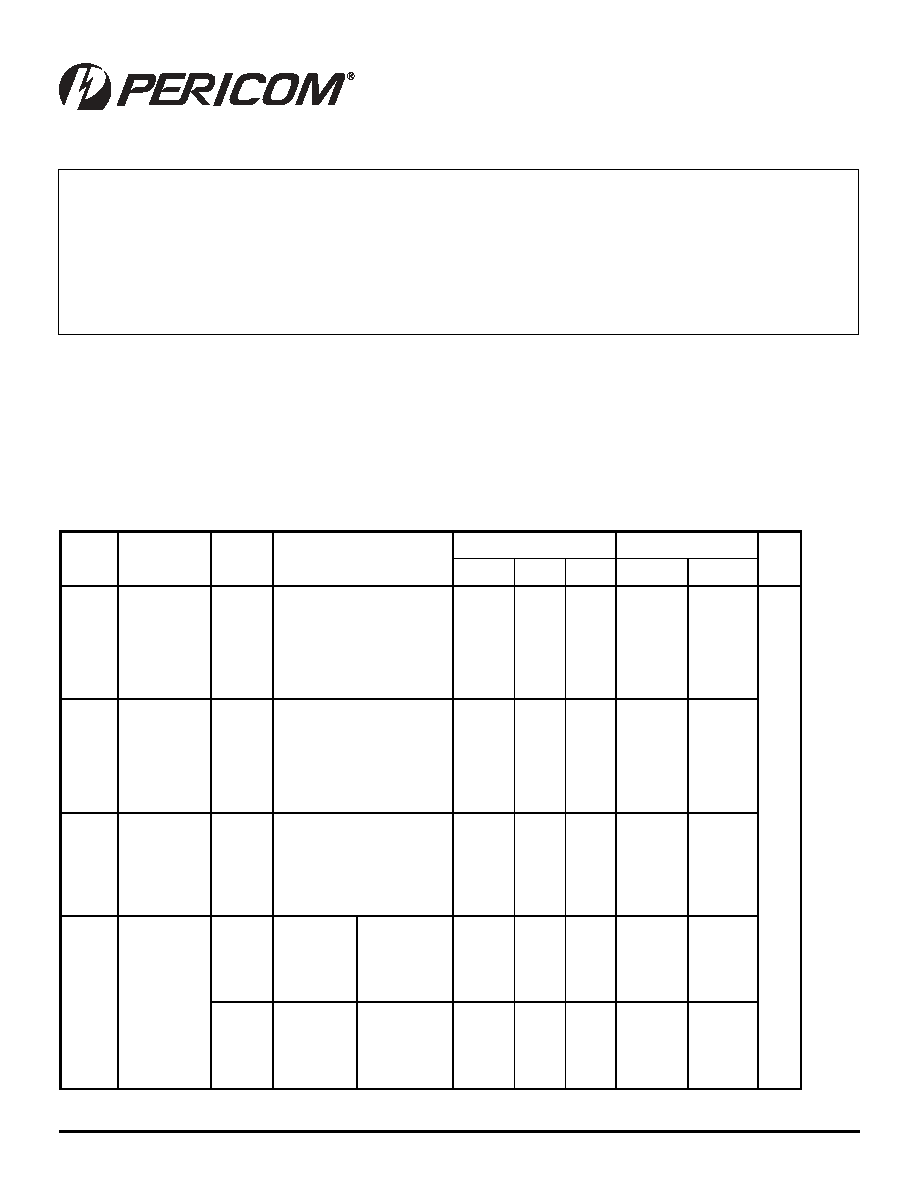
PI74STX2G14
Block Diagram
An
Yn
s
t
u
p
n
I
t
u
p
t
u
O
A
Y
L
H
H
L
Function Table
Note:
H = HIGH Logic Level
L = LOW Logic Level
Pin Description
s
e
m
a
N
n
i
P
n
o
i
t
p
i
r
c
s
e
D
n
A
s
t
u
p
n
I
n
Y
s
t
u
p
t
u
O
Recommended Operating Conditions
(1)
Note:
1. Unused inputs must be held HIGH or LOW. They may not float.
r
e
t
e
m
a
r
a
P
n
o
i
t
i
d
n
o
C
.
n
i
M
.
x
a
M
s
t
i
n
U
V
(
e
g
a
tl
o
V
y
l
p
p
u
S
C
C
)
5
6
.
1
5
.
5
V
V
(
e
g
a
tl
o
V
t
u
p
n
I
N
I
)
0
5
.
5
V
(
e
g
a
tl
o
V
t
u
p
t
u
O
T
U
O
)
0
V
C
C
e
r
u
t
a
r
e
p
m
e
T
g
n
it
a
r
e
p
O
0
4
5
8
C
°
d
n
a
e
s
i
R
t
u
p
n
I
t
(
e
m
i
T
ll
a
F
r
t,
f
)
V
C
C
,
V
8
.
1
=
V
2
.
0
±
V
5
.
2
0
0
2
V
/
s
n
V
C
C
,
V
3
.
3
=
V
3
.
0
±
0
0
1
V
C
C
,
V
0
.
5
=
V
5
.
0
±
0
5
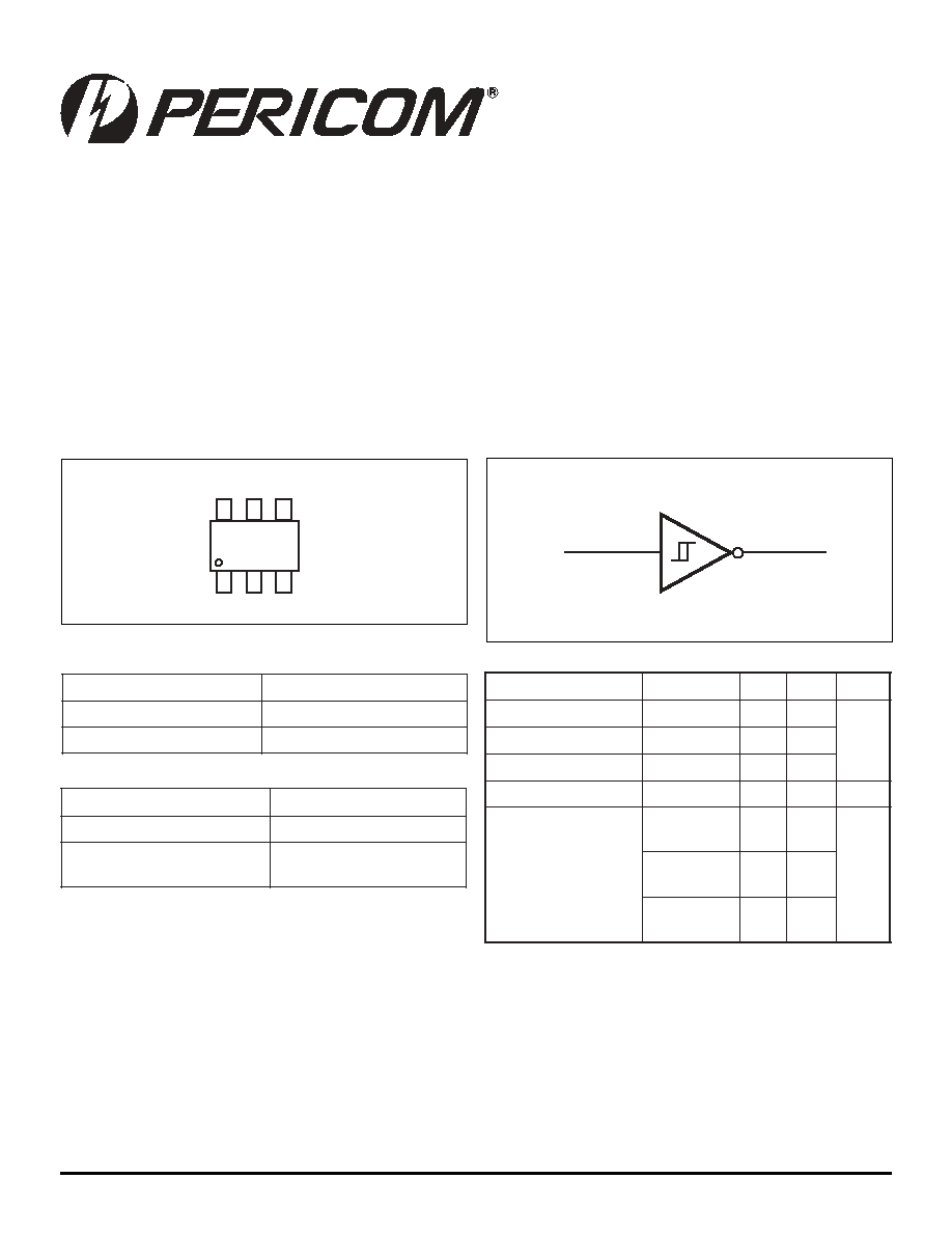
PI74STX2G14
GND
Y2
Y1 VCC
A2
A1
1
2
3
6
5
4
6-Pin
C
2
PS8644A 03/23/04
12345678901234567890123456789012123456789012345678901234567890121234567890123456789012345678901212345678901234567890123456789012123456789012
12345678901234567890123456789012123456789012345678901234567890121234567890123456789012345678901212345678901234567890123456789012123456789012
PI74STX2G14
SOTiny
TM
Gate STX Dual
Schmitt-Trigger Inverter
DC Electrical Characteristics
(Over supply voltage and operating temperature ranges, unless otherwise specified)
Supply Voltage (V
CC
) ......................................... 0.5V to +7V
DC Input Voltage (V
IN
(1)
) .................................... 0.5V to +7V
Voltage Range Applied to Any Output in the Power-Off State,
V
OUT
(1)
............................................................... 0.5V to +7V
Voltage Range Applied to Any Output in the High or Low State,
V
OUT
(1)
...................................................... 0.5V toV
CC
+0.5V
DC Input Diode Current (I
IK
) ....................... 50mA to 20mA
Absolute Maximum Ratings
Note:
Absolute maximum ratings are DC values beyond which the device may be damaged or have its useful life impaired. The datasheet
specifications should be met, without exception, to ensure that the system design is reliable over its power supply, temperature, and
output/input loading variables. Pericom does not recommend operation outside datasheet specifications.
1. The input negative voltage and output voltage ratings may be exceeded if the input and output current ratings are observed.
DC Output Diode Current (I
OK
) .................... 50mA to 20mA
DC Output Current (I
OUT
) ........................................... ±50mA
DC V
CC
/GND Current (I
CC
/I
GND
) ...............................±100mA
Storage Temperature (T
STG
) .......................... 65°C to +150°C
Junction Lead Temperature (IOS) ................................... 260°C
Power Dissipation SC70 ............................................... 150mW
Symbol
Parameter
V
CC
(V)
Conditions
TA = +°25C
TA = -40C to +8°5C
Units
Min.
Typ.
Max.
Min.
Max.
V
P
Positive
Threshold
Voltage
1.65
1.8
2.3
3.0
4.5
5.5
0.6
0.7
1.0
1.3
1.9
2.2
1.05
1.11
1.32
1.61
2.26
2.49
1.4
1.5
1.8
2.2
3.1
3.6
0.6
0.7
1.0
1.3
1.9
2.2
1.4
1.5
1.8
2.2
3.1
3.6
V
V
N
Negative
Threshold
Voltage
1.65
1.8
2.3
3.0
4.5
5.5
0.2
0.25
0.40
0.6
1.0
1.2
0.65
0.70
0.86
1.05
1.42
1.54
0.8
0.9
1.15
1.5
2.0
2.3
0.2
0.25
0.40
0.6
1.0
1.2
0.8
0.9
1.15
1.5
2.0
2.3
V
H
Hysteresis
Voltage
1.65
1.8
2.3
3.0
4.5
5.5
0.1
0.15
0.25
0.4
0.6
0.7
0.40
0.41
0.46
0.56
0.85
0.96
0.9
1.0
1.1
1.2
1.5
1.7
0.1
0.15
0.25
0.4
0.6
0.7
0.9
1.0
1.1
1.2
1.5
1.7
V
OH
HIGH Level
Output Voltage
1.65
1.8
2.3
3.0
4.5
V
IN
= V
IL
I
OH
= 100µA
1.55
1.7
2.2
2.9
4.4
1.65
1.8
2.3
3.0
4.5
1.55
1.7
2.2
2.9
4.4
1.65
2.3
3.0
3.0
4.5
I
OH
= 4mA
I
OH
= 8mA
I
OH
= 16mA
I
OH
= 24mA
I
OH
= 32mA
1.29
1.9
2.4
2.3
3.8
1.48
2.09
2.67
2.48
4.00
1.29
1.9
2.4
2.3
3.8
3
PS8644A 03/23/04
12345678901234567890123456789012123456789012345678901234567890121234567890123456789012345678901212345678901234567890123456789012123456789012
12345678901234567890123456789012123456789012345678901234567890121234567890123456789012345678901212345678901234567890123456789012123456789012
PI74STX2G14
SOTiny
TM
Gate STX Dual
Schmitt-Trigger Inverter
l
o
b
m
y
S
r
e
t
e
m
a
r
a
P
V
C
C
)
V
(
s
n
o
i
t
i
d
n
o
C
T
A
C
°
5
2
+
=
T
A
C
°
5
8
+
o
t
0
4
=
s
t
i
n
U
.
n
i
M
.
p
y
T
.
x
a
M
.
n
i
M
.
x
a
M
V
L
O
l
e
v
e
L
W
O
L
e
g
a
tl
o
V
t
u
p
t
u
O
5
6
.
1
8
.
1
3
.
2
0
.
3
5
.
4
V
N
I
V
=
H
I
I
L
O
A
µ
0
0
1
=
0
.
0
0
.
0
0
.
0
0
.
0
0
.
0
1
.
0
1
.
0
1
.
0
1
.
0
1
.
0
1
.
0
1
.
0
1
.
0
1
.
0
1
.
0
V
5
6
.
1
3
.
2
0
.
3
0
.
3
5
.
4
I
L
O
A
m
4
=
I
L
O
A
m
8
=
I
L
O
A
m
6
1
=
I
L
O
A
m
4
2
=
I
L
O
A
m
2
3
=
6
0
.
0
0
1
.
0
7
1
.
0
6
2
.
0
9
2
.
0
4
2
.
0
3
.
0
4
.
0
5
5
.
0
5
5
.
0
4
2
.
0
3
.
0
4
.
0
5
5
.
0
5
5
.
0
I
N
I
e
g
a
k
a
e
L
t
u
p
n
I
t
n
e
r
r
u
C
5
.
5
o
t
0
V
N
I
D
N
G
,
V
5
.
5
=
1
.
0
±
0
.
1
±
A
µ
I
F
F
O
f
f
O
r
e
w
o
P
t
n
e
r
r
u
C
e
g
a
k
a
e
L
0
.
0
V
N
I
V
r
o
T
U
O
V
5
.
5
=
1
±
0
1
±
I
C
C
y
l
p
p
u
S
t
n
e
c
s
e
i
u
Q
t
n
e
r
r
u
C
5
.
5
-
5
6
.
1
V
N
I
D
N
G
,
V
5
.
5
=
0
.
2
0
2
DC Electrical Characteristics
(Over supply voltage and operating temperature ranges, unless otherwise specified) (continued)
AC Electrical Characteristics
Notes:
3. C
PD
is defined as the value of the internal equivalent capacitance which is derived from dynamic operating current consumption
(I
CCD
) at no output loading and operating at 50% duty cycle (see Figure 2). C
PD
is related to I
CCD
dynamic operating current by
the expression: I
CCD
= (C
PD
)(V
CC
)(f
IN
) + (I
CC
static).
l
o
b
m
y
S
r
e
t
e
m
a
r
a
P
V
C
C
)
V
(
s
n
o
i
t
i
d
n
o
C
T
A
C
°
5
2
+
=
T
A
C
°
5
8
+
o
t
C
°
0
4
=
s
t
i
n
U
.
g
i
F
.
o
N
.
n
i
M
.
p
y
T
.
x
a
M
.
n
i
M
.
x
a
M
t
H
L
P
,
t
L
H
P
y
a
l
e
D
n
o
i
t
a
g
a
p
o
r
P
5
6
.
1
8
.
1
2
.
0
±
5
.
2
3
.
0
±
3
.
3
5
.
0
±
0
.
5
C
L
,
F
p
5
1
=
R
L
M
1
=
5
.
2
5
.
2
8
.
1
5
.
1
0
.
1
1
.
3
1
9
.
0
1
4
.
7
0
.
5
1
.
4
5
.
2
5
.
2
8
.
1
5
.
1
0
.
1
5
.
4
1
0
.
2
1
0
.
8
5
.
5
5
.
4
s
n
1
3
t
H
L
P
,
t
L
H
P
y
a
l
e
D
n
o
i
t
a
g
a
p
o
r
P
3
.
0
±
3
.
3
5
.
0
±
0
.
5
C
L
,
F
p
0
5
=
R
L
0
0
5
=
8
.
1
2
.
1
0
.
6
9
.
4
8
.
1
2
.
1
6
.
6
4
.
5
1
3
C
N
I
e
c
n
a
ti
c
a
p
a
C
t
u
p
n
I
0
1
.
2
F
p
C
D
P
n
o
i
t
a
p
i
s
s
i
D
r
e
w
o
P
e
c
n
a
ti
c
a
p
a
C
)
3
(
3
.
3
0
.
5
9
.
4
1
2
.
8
1
2
8.1
2.5
15.0
19.0
4
PS8644A 03/23/04
12345678901234567890123456789012123456789012345678901234567890121234567890123456789012345678901212345678901234567890123456789012123456789012
12345678901234567890123456789012123456789012345678901234567890121234567890123456789012345678901212345678901234567890123456789012123456789012
PI74STX2G14
SOTiny
TM
Gate STX Dual
Schmitt-Trigger Inverter
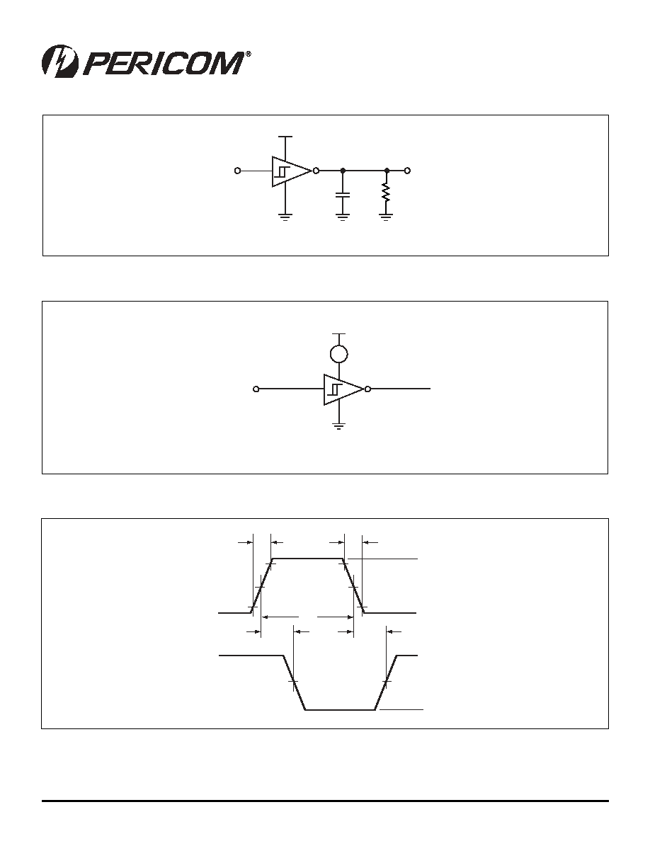
AC Loading and Waveforms
Figure 1. AC Test Circuit
Figure 2. I
CCD
Test Circuit
Figure 3. AC Waveforms
C
L
includes load and stray capacitance
Input PRR = 1.0 MHz; t
W
= 500ns
Input
R
L
C
L
V
CC
Output
Input = AC Waveform; t
r
= t
f
= 1.8ns;
PRR = Variable; Duty Cycle = 50%
Input
V
CC
A
V
OH
GND
Input
Output
t
W
t
PHL
t
r
= 3ns
t
f
= 3ns
t
PLH
V
OL
50%
50%
50%
50%
90%
90%
10%
10%
V
CC
5
PS8644A 03/23/04
12345678901234567890123456789012123456789012345678901234567890121234567890123456789012345678901212345678901234567890123456789012123456789012
12345678901234567890123456789012123456789012345678901234567890121234567890123456789012345678901212345678901234567890123456789012123456789012
PI74STX2G14
SOTiny
TM
Gate STX Dual
Schmitt-Trigger Inverter
Ordering Information
Pericom Semiconductor Corporation
1-800-435-2336 · http://www.pericom.com
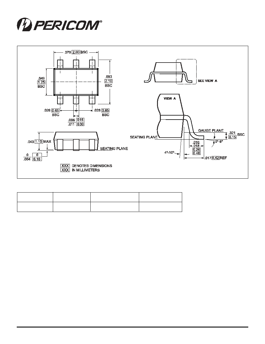
Packaging Mechanical: 6-Pin SC70 (C)
5
6
4
2
1
3
Notes:
1) Controlling dimensions in millimeters
2) Ref: JEDEC MO-203AB
Ordering Code
Package Code
Package Description
Top Marking
PI74STX2G14X
C
6-pin SC70
DC