DATASHEET SEARCH SITE | WWW.ALLDATASHEET.COM
1
PS8583A 09/27/04
12345678901234567890123456789012123456789012345678901234567890121234567890123456789012345678901212345678901234567890123456789012123456789012
12345678901234567890123456789012123456789012345678901234567890121234567890123456789012345678901212345678901234567890123456789012123456789012
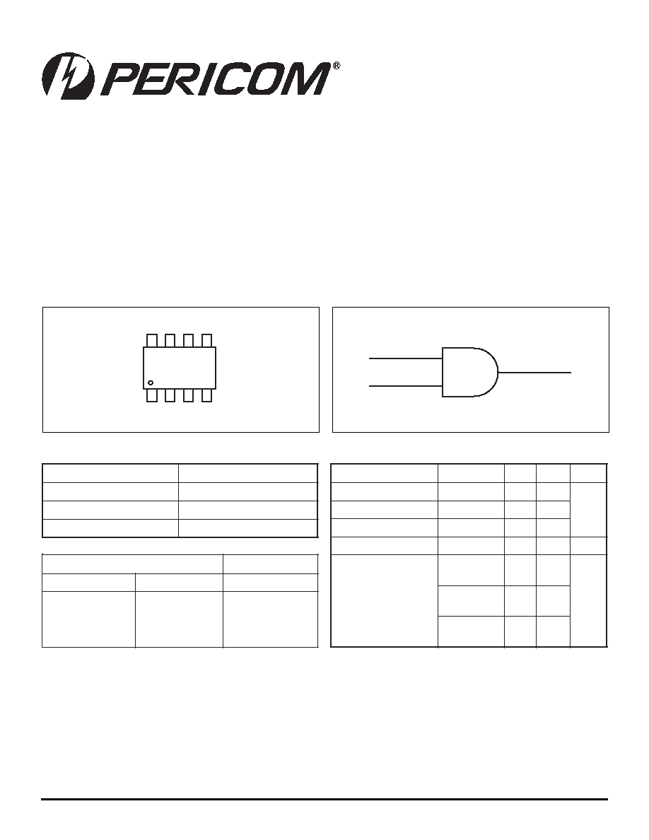
SOTiny
TM
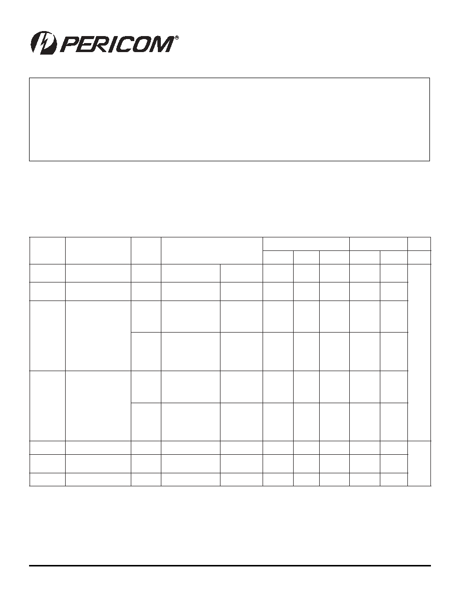
Gate STX
Dual 2-Input AND
Features
· High-Speed: t
PD
= 2.6ns typical into 50pF @ 5V V
CC
· Broad Operating Range: V
CC
= 1.65V 5.5V
· Power down high-impedance inputs/outputs
· High Output Drive: ±24mA at 3V V
CC
· Package: 8-pin space saving US8 (D)
8-pin space saving MSOP (U)
Description
Pericom Semiconductor's PI74STX2G08 is a dual 2-input
and gate that operates over the 1.65V to 5.5V V
CC
operating range.
PI74STX2G08
s
t
u
p
n
I
t
u
p
t
u
O
A
B
Y
L
L
H
H
L
H
L
H
L
L
L
H
Function Table
Note:
H = HIGH Logic Level
L = LOW Logic Level
Pin Description
s
e
m
a
N
n
i
P
n
o
i
t
p
i
r
c
s
e
D
n
A
s
t
u
p
n
I
n
B
s
t
u
p
n
I
n
Y
s
t
u
p
t
u
O
Recommended Operating Conditions
(1)
Note:
1. Unused inputs must be held HIGH or LOW. They may not float.
r
e
t
e
m
a
r
a
P
n
o
i
t
i
d
n
o
C
.
n
i
M
.
x
a
M
s
t
i
n
U
V
(
e
g
a
tl
o
V
y
l
p
p
u
S
C
C
)
5
6
.
1
5
.
5
V
V
(
e
g
a
tl
o
V
t
u
p
n
I
N
I
)
0
5
.
5
V
(
e
g
a
tl
o
V
t
u
p
t
u
O
T
U
O
)
0
V
C
C
e
r
u
t
a
r
e
p
m
e
T
g
n
it
a
r
e
p
O
0
4
5
8
C
°
d
n
a
e
s
i
R
t
u
p
n
I
t
(
e
m
i
T
ll
a
F
r
t,
f
)
V
C
C
,
V
8
.
1
=
V
2
.
0
±
V
5
.
2
0
0
2
V
/
s
n
V
C
C
,
V
3
.
3
=
V
3
.
0
±
0
0
1
V
C
C
,
V
0
.
5
=
V
5
.
0
±
0
5
Block Diagram
Pinout
An
Bn
Yn
A1
V
CC
Y1 B2 A2
Y2 GND
B1
1
2
3
4
8
7
6
5
8-Pin
D,U
2
PS8583A 09/27/04
12345678901234567890123456789012123456789012345678901234567890121234567890123456789012345678901212345678901234567890123456789012123456789012
12345678901234567890123456789012123456789012345678901234567890121234567890123456789012345678901212345678901234567890123456789012123456789012
PI74STX2G08
SOTiny
TM
Gate STX
Dual 2-Input AND
DC Electrical Characteristics
(Over supply voltage and operating temperature ranges, unless otherwise specified)
Supply Voltage (V
CC
) ........................................... 0.5V to +7V
DC Input Voltage (V
IN
)
(1) .....................................................................
0.5V to +7V
Voltage Range Applied to Any Output in the Power-Off State,
V
OUT
(1)
................................................................. 0.5V to +7V
Voltage Range Applied to Any Output in the High or Low State,
V
OUT
(1)
........................................................ 0.5V toV
CC
+0.5V
DC Input Diode Current (I
IK
) ......................... 50mA to 20mA
Absolute Maximum Ratings
Note:
Absolute maximum ratings are DC values beyond which the device may be damaged or have its useful life impaired. The datasheet
specifications should be met, without exception, to ensure that the system design is reliable over its power supply, temperature, and
output/input loading variables. Pericom does not recommend operation outside datasheet specifications.
1. The input negative voltage and output voltage ratings may be exceeded if the input and output current ratings are observed.
DC Output Diode Current (I
OK
) .................. 50mA to 20mA
DC Output Current (I
OUT
) ..........................................±50mA
DC V
CC
/GND Current (I
CC
/I
GND
) ............................. ±100mA
Storage Temperature (T
STG
) ........................ 65°C to +150°C
Junction Lead Temperature (IOS) .................................. 260°C
Power Dissipation: MSOP ......................................... 300mW
US8 ............................................ 200mW
l
o
b
m
y
S
r
e
t
e
m
a
r
a
P
V
C
C
)
V
(
s
n
o
i
t
i
d
n
o
C
T
A
C
°
5
2
+
=
T
A
C
°
5
8
+
o
t
C
°
0
4
=
.
n
i
M
.
p
y
T
.
x
a
M
.
n
i
M
.
x
a
M
s
t
i
n
U
V
H
I
e
g
a
tl
o
V
t
u
p
n
I
l
e
v
e
L
h
g
i
H
5
9
.
1
-
5
6
.
1
5
.
5
-
3
.
2
V
5
7
.
0
C
C
V
0
7
.
0
C
C
V
5
7
.
0
C
C
V
7
.
0
C
C
V
V
L
I
e
g
a
tl
o
V
t
u
p
n
I
l
e
v
e
L
w
o
L
5
9
.
1
-
5
6
.
1
5
.
5
-
3
.
2
V
5
2
.
0
C
C
V
3
.
0
C
C
V
5
2
.
0
C
C
V
0
3
.
0
C
C
V
H
O
t
u
p
t
u
O
l
e
v
e
L
h
g
i
H
e
g
a
tl
o
V
5
6
.
1
3
.
2
0
.
3
5
.
4
V
=
N
I
V
H
I
I
H
O
A
µ
0
0
1
=
5
5
.
1
2
.
2
9
.
2
4
.
4
5
6
.
1
3
.
2
0
.
3
5
.
4
5
5
.
1
2
.
2
9
.
2
4
.
4
5
6
.
1
3
.
2
0
.
3
0
.
3
5
.
4
I
H
O
A
m
4
=
I
H
O
A
m
8
=
I
H
O
A
m
6
1
=
I
H
O
A
m
4
2
=
I
H
O
A
m
2
3
=
9
2
.
1
9
.
1
4
.
2
3
.
2
8
.
3
0
5
.
1
0
1
.
2
9
6
.
2
1
5
.
2
2
0
.
4
9
2
.
1
9
.
1
4
.
2
3
.
2
8
.
3
V
L
O
t
u
p
t
u
O
l
e
v
e
L
w
o
L
e
g
a
tl
o
V
5
6
.
1
3
.
2
0
.
3
5
.
4
V
=
N
I
V
H
I
r
o V
L
I
I
H
O
A
µ
0
0
1
=
0
.
0
0
.
0
0
.
0
0
.
0
1
.
0
1
.
0
1
.
0
1
.
0
1
.
0
1
.
0
1
.
0
1
.
0
5
6
.
1
3
.
2
0
.
3
0
.
3
5
.
4
I
H
O
A
m
4
=
I
H
O
A
m
8
=
I
H
O
A
m
6
1
=
I
H
O
A
m
4
2
=
I
H
O
A
m
2
3
=
7
0
.
0
1
1
.
0
8
1
.
0
8
2
.
0
2
3
.
0
4
2
.
0
3
.
0
4
.
0
5
5
.
0
5
5
.
0
4
2
.
0
3
.
0
4
.
0
5
5
.
0
5
5
.
0
I
N
I
t
n
e
r
r
u
C
e
g
a
k
a
e
L
t
u
p
n
I
V
5
.
5
-
0
V
N
I
D
N
G
r
o
V
5
.
5
=
1
.
0
±
0
.
1
±
A
µ
I
F
F
O
e
g
a
k
a
e
L
f
f
O
r
e
w
o
P
t
n
e
r
r
u
C
0
.
0
V
N
I
V
r
o
T
U
O
V
5
.
5
=
1
±
0
1
±
I
C
C
t
n
e
r
r
u
C
y
l
p
p
u
S
t
n
e
c
s
e
i
u
Q
5
.
5
-
5
6
.
1
V
N
I
D
N
G
,
V
5
.
5
=
1
0
1
3
PS8583A 09/27/04
12345678901234567890123456789012123456789012345678901234567890121234567890123456789012345678901212345678901234567890123456789012123456789012
12345678901234567890123456789012123456789012345678901234567890121234567890123456789012345678901212345678901234567890123456789012123456789012
PI74STX2G08
SOTiny
TM
Gate STX
Dual 2-Input AND
l
o
b
m
y
S
s
r
e
t
e
m
a
r
a
P
V
C
C
)
V
(
s
n
o
i
t
i
d
n
o
C
T
A
C
°
5
2
+
=
T
A
C
°
5
8
+
o
t
C
°
0
4
=
s
t
i
n
U
g
i
F
o
N
.
n
i
M
.
p
y
T
.
x
a
M
.
n
i
M
.
x
a
M
t
,
H
L
P
t
L
H
P
y
a
l
e
D
n
o
it
a
g
a
p
o
r
P
5
1
.
0
±
8
.
1
2
.
0
±
5
.
2
3
.
0
±
3
.
3
5
.
0
±
0
.
5
C
L
,
F
p
5
1
=
R
L
m
h
o
M
1
=
0
.
2
0
.
1
8
.
0
5
.
0
5
.
0
1
8
.
5
9
.
3
1
.
3
0
.
2
0
.
1
8
.
0
5
.
0
0
.
1
1
2
.
6
3
.
4
3
.
3
s
n
1
3
t
,
H
L
P
t
L
H
P
y
a
l
e
D
n
o
it
a
g
a
p
o
r
P
3
.
0
±
3
.
3
5
.
0
±
0
.
5
C
L
,
F
p
0
5
=
R
L
s
m
h
O
0
0
5
=
2
.
1
8
.
0
8
.
4
7
.
3
2
.
1
8
.
0
2
.
5
0
.
4
1
3
C
N
I
e
c
n
a
ti
c
a
p
a
C
t
u
p
n
I
0
5
.
2
F
p
C
D
P
n
o
it
a
p
i
s
s
i
D
r
e
w
o
P
e
c
n
a
ti
c
a
p
a
C
)
2
(
3
.
3
0
.
5
5
1
9
1
2
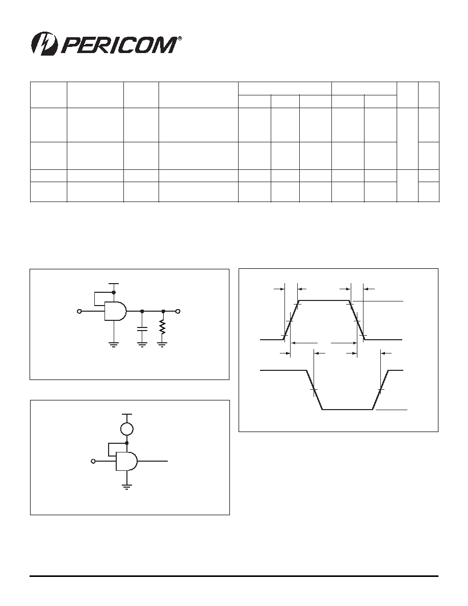
AC Loading and Waveforms
Figure 1. AC Test Circuit
Figure 2. I
CCD
Test Circuit
Figure 3. AC Waveforms
Input = AC Waveform; t
r
= t
f
= 1.8ns;
PRR = 10 MHz; Duty Cycle = 50%
Input
V
CC
A
V
OH
GND
Input
Output
t
W
t
PHL
t
r
= 3ns
t
f
= 3ns
t
PLH
V
OL
50%
50%
50%
50%
90%
90%
10%
10%
V
CC
AC Electrical Characteristics
Notes:
2. C
PD
is defined as the value of the internal equivalent capacitance which is derived from dynamic operating current consumption
(I
CCD
) at no output loading and operating at 50% duty cycle (see Figure 2). C
PD
is related to I
CCD
dynamic operating current by
the expression: I
CCD
= (C
PD
)(V
CC
)(f
IN
) + (I
CC
static).
C
L
includes load and stray capacitance
Input PRR = 1.0 MHz; t
W
= 500ns
Input
R
L
C
L
V
CC
Output
4
PS8583A 09/27/04
12345678901234567890123456789012123456789012345678901234567890121234567890123456789012345678901212345678901234567890123456789012123456789012
12345678901234567890123456789012123456789012345678901234567890121234567890123456789012345678901212345678901234567890123456789012123456789012
PI74STX2G08
SOTiny
TM
Gate STX
Dual 2-Input AND
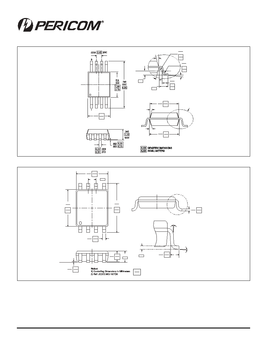
Packaging Mechanical: 8-Pin US8 (D)
15
°
MAX
15
°
MAX
Detail A
Detail A
.112
.120
2.85
3.05
.114
.122
2.90
3.10
.114
.122
2.90
3.10
.010
0
°
- 6
°
15° Max.
15° Max.
0.25
Gauge
Plane
.003
.012
.016
.028
.037
0.40
0.70
0.95
REF
0.07
0.30
.003
.012
0.07
0.30
Packaging Mechanical: 8-Pin MSOP (U)
See Detail A
Detail A
.086
.094
2.20
2.40
.075
.083
1.90
2.10
.02 0.50
.118
.126
3.00
3.20
.007
.011
0.17
0.27
.000
.004
0.00
0.10
.024
.031
0.60
0.80
Seating Plane
.035
0.90
.003
.009
0.08
0.23
Gage Plane
.005
0.12
BSC
MAX
0° - 6°
10° REF
.008
.014
0.20
0.35
X.XX
X.XX
DENOTES DIMENSIONS
IN MILLIMETERS
5
PS8583A 09/27/04
12345678901234567890123456789012123456789012345678901234567890121234567890123456789012345678901212345678901234567890123456789012123456789012
12345678901234567890123456789012123456789012345678901234567890121234567890123456789012345678901212345678901234567890123456789012123456789012
PI74STX2G08
SOTiny
TM
Gate STX
Dual 2-Input AND
Pericom Semiconductor Corporation · 1-800-435-2336 · http://www.pericom.com
Ordering Information
Notes:
1. Thermal characteristics can be found on the company web site at www.pericom.com/packaging/
2. X = Tape and reel
Ordering Code
Package Code
Package Description
PI74SXT2G08UX
U
8-pin MSOP
PI74SXT2G08UEX
U
Pb-free & Green, 8-pin MSOP
PI74SXT2G08DX
D
8-pin US8
PI74SXT2G08DEX
D
Pb-free & Green, 8-pin US8