Vcx16245
1
PS8325 09/14/98
Product Description
Pericom Semiconductors PI74VCX series of logic circuits are
produced in the Companys advanced 0.35 micron CMOS
technology, achieving industry leading speed.
The PI74VCX16245 is a 16-bit bidirectional transceiver designed
for asynchronous two-way communication between data buses.
The direction control input pin (xDIR) determines the direction of
data flow through the bidirectional transceiver. The Direction and
Output Enable controls are designed to operate this device as either
two independent 8-bit transceivers or one 16-bit transceiver. The
output enable (OE) input, when HIGH, disables both A and B ports
by placing them in HIGH Z condition.
To ensure the high-impedance state during power up or power
down, OE should be tied to Vcc through a pull-up resistor; the
minimum value of the resistor is determined by the current sinking
ability of the driver.
The PI74VCX family is I/O Tolerant, allowing it to operate in
mixed 1.8V/3.6V systems.
12345678901234567890123456789012123456789012345678901234567890121234567890123456789012345678901212345678901234567890123456789012123456789012
12345678901234567890123456789012123456789012345678901234567890121234567890123456789012345678901212345678901234567890123456789012123456789012
Product Features
�
The PI74VCX family is designed for low voltage operation
V
DD
= 1.8V to 3.6V
�
3.6V I/O Tolerant Inputs and Outputs
�
Supports Live Insertion
�
Balanced output drive, �24mA
�
Uses patented Noise Reduction Circuitry
�
Typical V
OLP
(Output Ground Bounce)
< 0.6V at V
DD
= 2.5V, T
A
= 25�C
�
Typical V
OHV
(Output V
OH
Undershoot)
< -0.6V at V
DD
= 2.5V, T
A
= 25�C
�
Power-Off High Impedance inputs and outputs
�
Industrial operation at 40�C to +85�C
�
Packages available:
48-pin 240 mil. wide plastic TSSOP (A)
48-pin 300 mil. wide plastic SSOP (V)
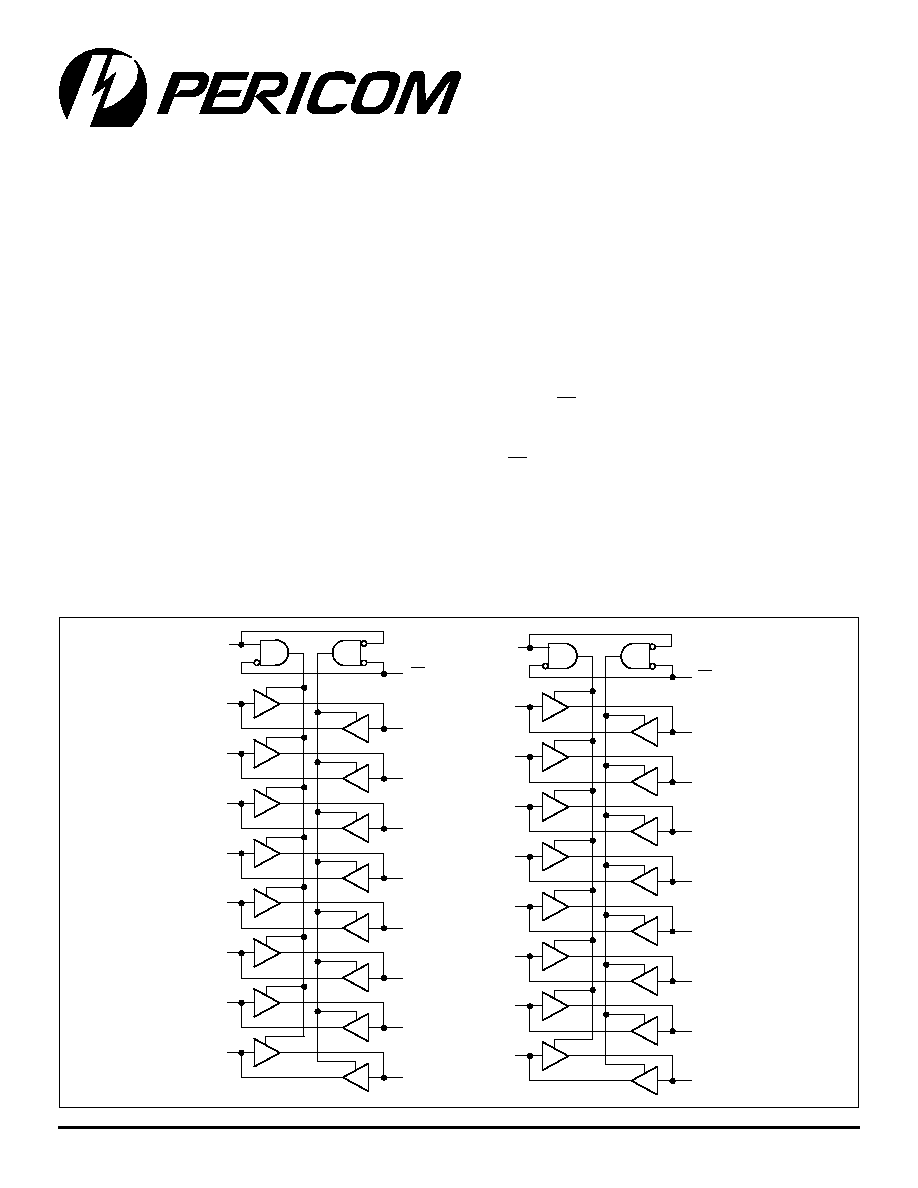
PI74VCX16245
2.5V 16-Bit Bidirectional Transceiver
with 3-State Outputs
Logic Block Diagram
1B
0
1A
0
1OE
1DIR
1B
1
1A
1
1B
2
1A
2
1B
3
1A
3
1B
4
1A
4
1B
5
1
A
5
1B
6
1A
6
1B
7
1A
7
2
B
0
2
A
0
2
OE
2
DIR
2
B
1
2
A
1
2
B
2
2
A
3
2
B
3
2
A
4
2
B
4
2
A
5
2
B
5
2
A
6
2
B
6
2
A
7
2
B
7
2
A
8
2
PS8325 09/14/98
PI74VCX16245
2.5V 16-Bit Bidirectional Transceiver with 3-State Outputs
12345678901234567890123456789012123456789012345678901234567890121234567890123456789012345678901212345678901234567890123456789012123456789012
s
t
u
p
n
I
)
1
(
s
t
u
p
t
u
O
)
1
(
E
O
x
R
I
D
x
L
L
A
s
u
B
o
t
a
t
a
D
B
s
u
B
L
H
B
s
u
B
o
t
a
t
a
D
A
s
u
B
H
X
e
t
a
t
S
Z
h
g
i
H
e
m
a
N
n
i
P
n
o
it
p
i
r
c
s
e
D
E
O
x
)
W
O
L
e
v
it
c
A
(
st
u
p
n
I
el
b
a
n
E
t
u
p
t
u
O
E
T
A
T
S
-
3
R
I
D
x
t
u
p
n
I
l
o
rt
n
o
C
n
o
it
c
e
ri
D
x
A
x
st
u
p
n
I
E
T
A
T
S
-
3
r
o
st
u
p
n
I
A
e
d
i
S
x
B
x
st
u
p
t
u
O
E
T
A
T
S
-
3
r
o
st
u
p
n
I
B
e
d
i
S
D
N
G
d
n
u
o
r
G
V
C
C
r
e
w
o
P
1
2
3
4
5
6
7
8
9
48
10
47
11
46
12
45
13
44
14
43
15
42
16
41
17
40
18
39
19
38
20
37
21
36
22
35
23
34
24
33
32
31
30
29
28
27
26
25
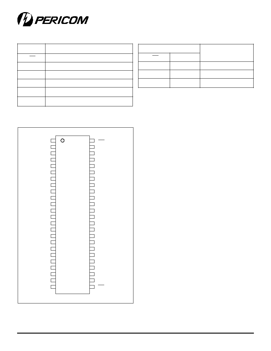
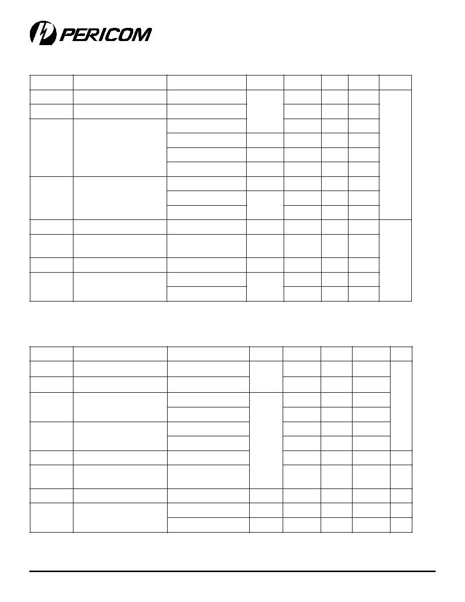
Product Pin Description
Truth Table
(1)
Notes:
1.
H = High Signal Level
L = Low Signal Level
X = Don't Care or Irrelevant
Z = High Impedance
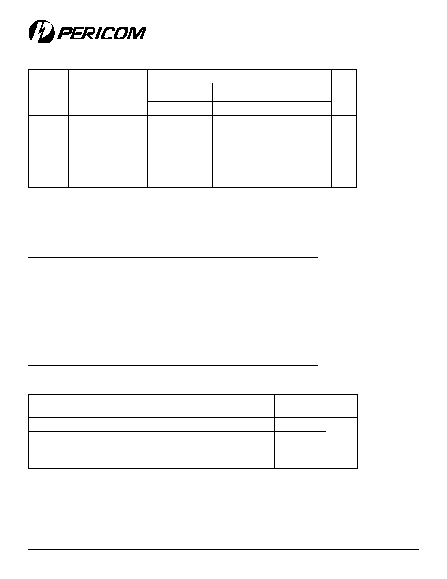
Product Pin Configuration
48-PIN
A48
V48
1OE
1A0
1A1
GND
1A2
1A3
VCC
1A4
1A5
GND
1A6
1A7
2A0
2A1
GND
2A2
2A3
VCC
2A4
2A5
GND
2A6
2A7
2OE
1DIR
1B0
1B1
GND
1B2
1B3
VCC
1B4
1B5
GND
1B6
1B7
2B0
2B1
GND
2B2
2B3
VCC
2B4
2B5
GND
2B6
2B7
2DIR
3
PS8325 09/14/98
12345678901234567890123456789012123456789012345678901234567890121234567890123456789012345678901212345678901234567890123456789012123456789012
PI74VCX16245
2.5V 16-Bit Bidirectional Transceiver with 3-State Outputs
Note:
Stresses greater than those listed under MAXIMUM
RATINGS may cause permanent damage to the device.
This is a stress rating only and functional operation of the
device at these or any other conditions above those indi-
cated in the operational sections of this specification is not
implied. Exposure to absolute maximum rating conditions
f
o
r
extended periods may affect reliability.
Supply Voltage Range, V
DD ................................................
�0.5V to 4.6V
Input Voltage Range, V
I .........................................................
-0.5V to 4.6V
Output Voltage Range, V
O
(3-Stated) .......................... -0.5V to 4.6V
Output Voltage Range, V
O
(1)
(Active) ............ �0.5V to V
DD
+ 0.5V
DC Input Diode Current (I
IK
) V
I
< 0V .................................... -50mA
DC Output Diode Current (I
OK
)
V
O
< 0V ................................................................................ -50mA
V
O
> V
DD ............................................................................................
-50mA
DC Output Source/Sink Current (I
OH
/I
OL
) ............................ �50mA
DC V
DD
or GND Current per Supply Pin (I
CC
or GND) .... �100mA
Storage Temperature Range, T
STG
............................ �65
�
C to150
�
C
Recommended Operating Conditions
(2)
Maximum Ratings
(Above which the useful life may be impaired. For user guidelines, not tested.)
Notes:
1. Absolute maximum of I
O
must be observed
2. Unused control inputs must be held HIGH or LOW to prevent them from floating
3. As measured between 0.8V and 2.0V, V
DD
= 3.0V
s
r
e
t
e
m
a
r
a
P
n
o
it
p
i
r
c
s
e
D
.
n
i
M
.
x
a
M
s
ti
n
U
V
D
D
e
g
a
tl
o
v
y
l
p
p
u
S
g
n
it
a
r
e
p
O
8
.
1
6
.
3
V
y
l
n
O
n
o
it
n
e
t
e
R
a
t
a
D
2
.
1
6
.
3
V
I
e
g
a
tl
o
v
t
u
p
n
I
3
.
0
-
6
.
3
V
O
e
g
a
tl
o
v
t
u
p
t
u
O
e
t
a
t
S
e
v
it
c
A
0
V
D
D
e
t
a
t
S
ff
O
0
6
.
3
I
n
i
t
n
e
rr
u
c
t
u
p
t
u
O
H
O
I/
L
O
V
D
D
V
6
.
3
o
t
V
0
.
3
=
V
D
D
V
7
.
2
o
t
V
3
.
2
=
V
D
D
V
8
.
1
=
4
2
�
8
1
�
6
�
A
m
D /tDv
e
t
a
r
ll
a
f
r
o
e
si
r
n
o
it
si
s
n
a
rt
t
u
p
n
I
)
3
(
0
0
1
V
/
s
n
T
A
e
r
u
t
a
r
e
p
m
e
t
ri
a
-
e
e
rf
g
n
it
a
r
e
p
O
- 0
4
5
8
C
�
4
PS8325 09/14/98
PI74VCX16245
2.5V 16-Bit Bidirectional Transceiver with 3-State Outputs
12345678901234567890123456789012123456789012345678901234567890121234567890123456789012345678901212345678901234567890123456789012123456789012
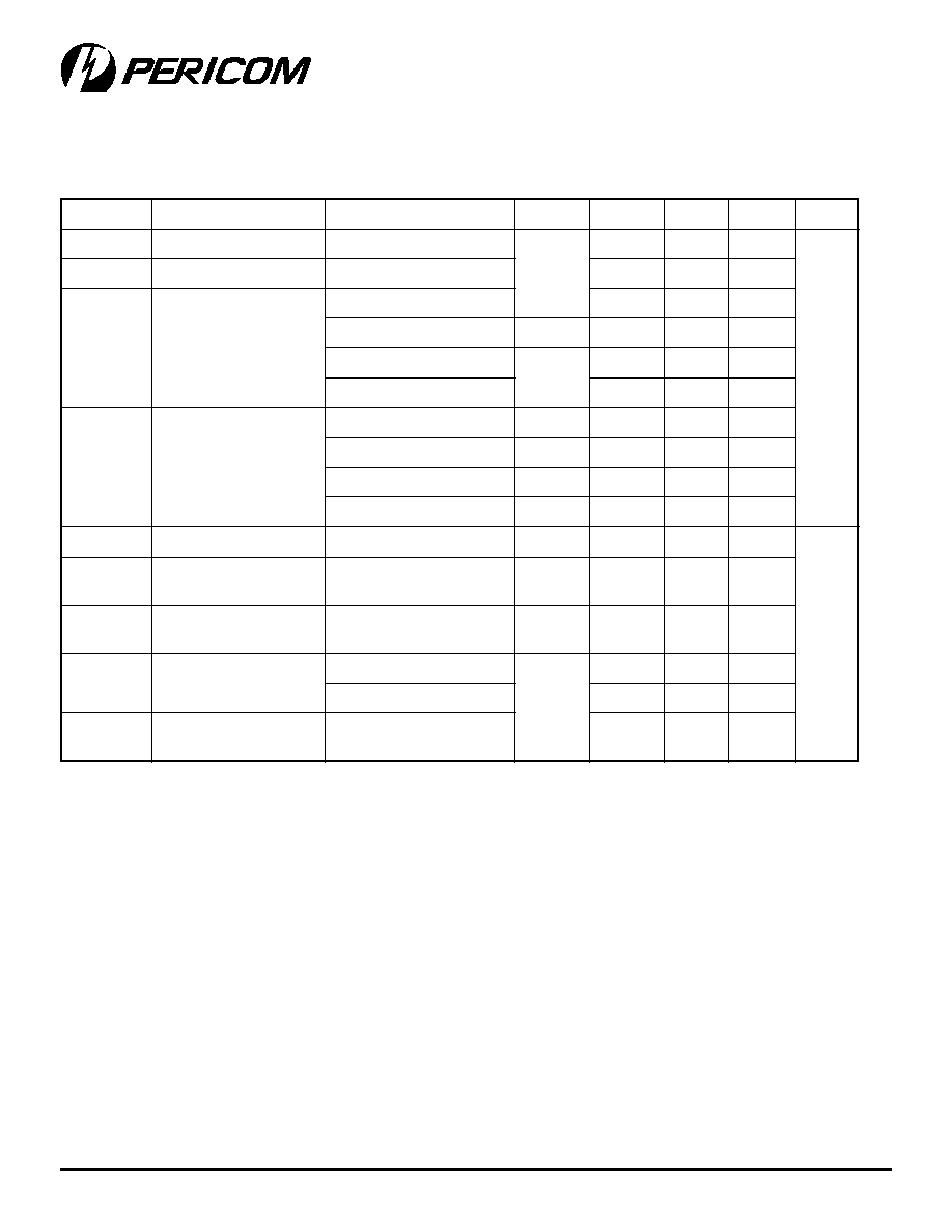
Electrical Characteristics over Recommended Operating Free-Air Temperature Range
(unless otherwise noted)
DC Characteristics (2.7V < V
DD
3.6V)
s
r
e
t
e
m
a
r
a
P
n
o
it
p
i
r
c
s
e
D
s
n
o
it
i
d
n
o
C
V
D
D
.
n
i
M
.
p
y
T
.
x
a
M
s
ti
n
U
V
H
I
e
g
a
tl
o
V
t
u
p
n
I
l
e
v
e
L
H
G
I
H
6
.
3
-
7
.
2
0
.
2
V
V
L
I
e
g
a
tl
o
V
t
u
p
n
I
l
e
v
e
L
W
O
L
8
.
0
V
H
O
l
e
v
e
L
H
G
I
H
e
g
a
tl
o
V
t
u
p
t
u
O
I
H
O
= - 0
0
1 mA
V
D
D
2
.
0
-
I
H
O
= -
A
m
2
1
7
.
2
2
.
2
I
H
O
= -
A
m
8
1
0
.
3
4
.
2
I
H
O
= -
A
m
4
2
2
.
2
V
L
O
l
e
v
e
L
W
O
L
e
g
a
tl
o
V
t
u
p
t
u
O
I
L
O
0
0
1
=
mA
6
.
3
-
7
.
2
2
.
0
I
L
O
A
m
2
1
=
7
.
2
4
.
0
I
L
O
A
m
8
1
=
0
.
3
4
.
0
I
L
O
A
m
4
2
=
5
5
.
0
I
I
t
n
e
rr
u
C
e
g
a
k
a
e
L
t
u
p
n
I
V
O � V
I
6
.
3
�
V
6
.
3
-
7
.
2
0
.
5
�
mA
I
Z
O
E
T
A
T
S
-
3
e
g
a
k
a
e
L
t
u
p
t
u
O
0 � V
O
�
V
6
.
3
V
I
V
=
H
I
V
r
o
L
I
6
.
3
-
7
.
2
0
1
�
I
F
F
O
F
F
O
-r
e
w
o
P
t
n
e
rr
u
C
e
g
a
k
a
e
L
0 � V
(
I
V
,
O
) �
V
6
.
3
0
0
1
I
D
D
t
n
e
rr
u
C
y
l
p
p
u
S
t
n
e
c
s
ei
u
Q
V
I
V
=
D
D
D
N
G
o
t
6
.
3
-
7
.
2
0
2
V
D
D
� V
(
I
V
,
O
) �
V
6
.
3
0
2
�
DI
D
D
I
n
i
e
s
a
e
r
c
n
I
D
D
t
u
p
n
i
r
e
p
V
H
I
V
=
D
D
,
V
6
.
0
-
V
t
a
st
u
p
n
i
r
e
h
t
O
D
D
D
N
G
r
o
0
5
7
5
PS8325 09/14/98
12345678901234567890123456789012123456789012345678901234567890121234567890123456789012345678901212345678901234567890123456789012123456789012
PI74VCX16245
2.5V 16-Bit Bidirectional Transceiver with 3-State Outputs
s
r
e
t
e
m
a
r
a
P
n
o
it
p
i
r
c
s
e
D
s
n
o
it
i
d
n
o
C
V
D
D
.
n
i
M
.
p
y
T
.
x
a
M
s
ti
n
U
V
H
I
e
g
a
tl
o
V
t
u
p
n
I
l
e
v
e
L
H
G
I
H
7
.
2
-
3
.
2
6
.
1
V
V
L
I
e
g
a
tl
o
V
t
u
p
n
I
l
e
v
e
L
W
O
L
7
.
0
V
H
O
l
e
v
e
L
H
G
I
H
e
g
a
tl
o
V
t
u
p
t
u
O
I
H
O
0
0
1
-
=
mA
V
D
D
2
.
0
-
I
H
O
A
m
6
-
=
3
.
2
0
.
2
I
H
O
A
m
2
1
-
=
8
.
1
I
H
O
A
m
8
1
-
=
7
.
1
V
L
O
l
e
v
e
L
W
O
L
e
g
a
tl
o
V
t
u
p
t
u
O
I
L
O
0
0
1
=
mA
7
.
2
-
3
.
2
2
.
0
I
L
O
A
m
2
1
=
3
.
2
4
.
0
I
L
O
A
m
8
1
=
6
.
0
I
I
t
n
e
rr
u
C
e
g
a
k
a
e
L
t
u
p
n
I
V
0 � 1
V �
V
6
.
3
7
.
2
-
3
.
2
0
.
5
�
mA
I
Z
O
e
g
a
k
a
e
L
t
u
p
t
u
O
E
T
A
T
S
-
3
0 � V
O
�
V
6
.
3
V
I
V
=
H
I
V
r
o
L
I
7
.
2
-
3
.
2
0
1
�
I
F
F
O
t
n
e
rr
u
C
e
g
a
k
a
e
L
F
F
O
-r
e
w
o
P
0 � V
(
I
V
,
O
) �
V
6
.
3
0
0
1
I
D
D
t
n
e
rr
u
C
y
l
p
p
u
S
t
n
e
c
s
ei
u
Q
V
I
V
=
D
D
D
N
G
r
o
7
.
2
-
3
.
2
0
2
V
D
D
(
�
)
0
V
,
1
V
6
.
3
�
V
0
2
�
DC Characteristics
(2.3V
V
DD
2.7V)
Electrical Characteristics over Recommended Operating Free-Air Temperature Range
DC Characteristics
(1.8V
V
DD
2.3V)
s
r
e
t
e
m
a
r
a
P
n
o
it
p
i
r
c
s
e
D
s
n
o
it
i
d
n
o
C
V
D
D
.
n
i
M
.
p
y
T
.
x
a
M
s
ti
n
U
V
H
I
e
g
a
tl
o
V
t
u
p
n
I
l
e
v
e
L
H
G
I
H
3
.
2
-
8
.
1
V
x
7
.
0
D
D
V
V
L
I
e
g
a
tl
o
V
t
u
p
n
I
l
e
v
e
L
W
O
L
V
x
2
.
0
D
D
V
H
O
e
g
a
tl
o
V
t
u
p
t
u
O
l
e
v
e
L
H
G
I
H
I
H
O
A
m
0
0
1
-
=
8
.
1
V
D
D
2
.
0
-
I
H
O
A
m
6
-
=
4
.
1
V
L
O
e
g
a
tl
o
V
t
u
p
t
u
O
l
e
v
e
L
W
O
L
I
L
O
A
m
0
0
1
=
2
.
0
I
H
O
A
m
6
-
=
3
.
0
I
I
t
n
e
rr
u
C
e
g
a
k
a
e
L
t
u
p
n
I
V
0 � 1
V �
V
6
.
3
0
.
5
�
I
Z
O
e
g
a
k
a
e
L
t
u
p
t
u
O
e
t
a
t
S
-
3
V
0 � 0
V �
V
6
.
3
V
I
V
=
H
I
V
r
o
L
I
0
1
�
I
F
F
O
t
n
e
rr
u
C
e
g
a
k
a
e
L
F
F
O
-r
e
w
o
P
V
0
(
�
)
0
V
,
1
V
�
V
6
.
3
0
0
1
A
m
I
D
D
t
n
e
rr
u
C
y
l
p
p
u
S
t
n
e
c
s
ei
u
Q
V
I
V
=
D
D
D
N
G
r
o
8
.
1
0
2
V
D
D
(
�
)
0
V
,
1
V
�
V
6
.
3
8
.
1
0
2
�
6
PS8325 09/14/98
PI74VCX16245
2.5V 16-Bit Bidirectional Transceiver with 3-State Outputs
12345678901234567890123456789012123456789012345678901234567890121234567890123456789012345678901212345678901234567890123456789012123456789012
l
o
b
m
y
S
s
r
e
t
e
m
a
r
a
P
T
A
C
,
C
�
5
8
+
o
t
C
�
0
4
-
=
L
R
,
F
p
0
3
=
L
0
0
5
=
W
s
ti
n
U
V
D
D
V
3
.
0
�
V
3
.
3
=
V
D
D
V
2
.
0
�
V
5
.
2
=
V
D
D
V
8
.
1
=
.
n
i
M
.
x
a
M
.
n
i
M
.
x
a
M
.
n
i
M
.
x
a
M
t
L
H
P
t
,
H
L
P
y
al
e
D
p
o
r
P
8
.
0
5
.
2
0
.
1
2
.
3
5
.
1
7
.
5
s
n
t
L
Z
P
t
,
H
Z
P
e
m
i
T
el
b
a
n
E
t
u
p
t
u
O
8
.
0
8
.
3
0
.
1
9
.
4
5
.
1
5
.
7
t
Z
L
P
t
,
Z
H
P
e
m
i
T
el
b
a
si
D
t
u
p
t
u
O
8
.
0
7
.
3
0
.
1
2
.
4
5
.
1
5
.
5
t
L
H
S
O
t
H
L
S
O
t
u
p
t
u
O
o
t
t
u
p
t
u
O
w
e
k
S
)
2
(
5
.
0
5
.
0
5
.
0
AC Electrical Characteristics
Notes:
1. For C
L
= 50pF, add approximately 300ps to the maximum AC specification
2. Skew is defined as the absolute value of the difference between the actual propagation delay for any two separate
outputs of the same device. The specification applies to any outputs switching in the same direction, either HIGH
or LOW (t
OSHL
)
or LOW to HIGH (t
OSLH
).
Dynamic Switching Characteristics
Capacitance
sl
o
b
m
y
S
s
r
e
t
e
m
a
r
a
P
s
n
o
it
i
d
n
o
C
T
A
C
�
5
2
+
=
l
a
c
i
p
y
T
s
ti
n
U
C
N
I
e
c
n
a
ti
c
a
p
a
C
t
u
p
n
I
V
D
D
V
,
V
3
.
3
r
o
V
5
.
2
,
8
.
1
=
I
V
r
o
V
0
=
D
D
6
F
p
C
T
U
O
e
c
n
a
ti
c
a
p
a
C
t
u
p
t
u
O
V
I
V
r
o
V
0
=
D
D
V
,
D
D
V
3
.
3
r
o
V
5
.
2
,
V
8
.
1
=
7
C
D
P
n
o
it
a
p
i
s
si
D
r
e
w
o
P
e
c
n
a
ti
c
a
p
a
C
V
I
V
r
o
V
0
=
D
D
z
H
M
0
1
=
F
,
V
D
D
V
3
.
3
r
o
V
5
.
2
,
V
8
.
1
=
0
2
l
o
b
m
y
S
s
r
e
t
e
m
a
r
a
P
s
n
o
it
i
d
n
o
C
V
D
D
T
A
l
a
c
i
p
y
T
C
�
5
2
+
=
s
ti
n
U
V
P
L
O
t
u
p
t
u
O
t
ei
u
Q
V
k
a
e
P
ci
m
a
n
y
D
L
O
C
L
F
p
0
3
=
V
H
I
V
=
D
D
V
L
I
V
0
=
8
.
1
5
.
2
3
.
3
5
2
.
0
6
.
0
8
.
0
V
V
V
L
O
t
u
p
t
u
O
t
ei
u
Q
V
y
el
l
a
V
ci
m
a
n
y
D
L
O
C
L
F
p
0
3
=
V
H
I
V
=
D
D
V
L
I
V
0
=
8
.
1
5
.
2
3
.
3
5
2
.
0
-
6
.
0
-
8
.
0
-
V
V
H
O
t
u
p
t
u
O
t
ei
u
Q
V
y
el
l
a
V
ci
m
a
n
y
D
H
O
C
L
F
p
0
3
=
V
H
I
V
=
D
D
V
L
I
V
0
=
8
.
1
5
.
2
3
.
3
5
.
1
9
.
1
2
.
2
7
PS8325 09/14/98
12345678901234567890123456789012123456789012345678901234567890121234567890123456789012345678901212345678901234567890123456789012123456789012
PI74VCX16245
2.5V 16-Bit Bidirectional Transceiver with 3-State Outputs
Test Circuits and Switching Waveforms
Parameter Measurement Information (V
DD
= 1.8V - 3.6V)
Setup, Hold, and Release Timing
Pulse Width
Switch Position
Propagaton Delay
Enable Disable Timing
Notes:
A. C
L
includes probe and jig capacitance.
B. Waveform 1 is for an output with internal conditions such that
the output is LOW except when disabled by the output control.
Waveform 2 is for an output with internal conditions such that
the output is HIGH except when disabled by the output
control.
C. All input pulses are supplied by generators having the follow
ing characteristics:
P
RR
10 MHz, Z
O
= 50
,
t
R
2ns,
t
F
2ns,
measured from 10% to 90%, unless otherwise specified.
D. The outputs are measured one at a time with one transition per
measurement.
Pericom Semiconductor Corporation
2380 Bering Drive � San Jose, CA 95131 � 1-800-435-2336 � Fax (408) 435-1100 � http://www.pericom.com
Output
Control
(Active LOW)
Output
Waveform 2
S1 at GND
(see Note B)
t
PZL
t
PLZ
V
DD
0V
V
DD
V
OL
0V
Output
Waveform 1
S1 at 2xV
DD
(see Note B)
+0.15V
-0.15V
V
OH
V
DD
t
PHZ
t
PZH
V
DD/2
V
DD/2
V
DD
/2
C
L
R
1
500
30pF
From Output
Under Test
GND
2 x V
DD
Open
(See Note A)
R
L
500
Data
Input
t
H
V
DD
t
SU
0V
Timing
Input
V
DD
0V
V
DD/2
V
DD/2
Low-High-Low
Pulse
t
W
High-Low-High
Pulse
V
DD
0V
V
DD
0V
V
DD/2
V
DD/2
Input
Opposite Phase
Input Transition
t
PLH
t
PHL
t
PLH
t
PHL
V
DD
0V
V
DD
V
OL
V
DD
0V
Output
V
DD/2
V
DD/2
V
DD/2
t
s
e
T
1
S
t
D
P
n
e
p
O
t
Z
L
P
/t
L
Z
P
x
2 V
D
D
t
Z
H
P
/t
H
Z
P
D
N
G