 | –≠–ª–µ–∫—Ç—Ä–æ–Ω–Ω—ã–π –∫–æ–º–ø–æ–Ω–µ–Ω—Ç: PI7AT04 | –°–∫–∞—á–∞—Ç—å:  PDF PDF  ZIP ZIP |

1
PS8588C 08/02/04
Features
5V and 3.3V Line Clamping
Near Zero Quiescent Supply Current: 10µA Maximum
≠ Active circuit clamping
Low Capacitance: 5pF (typ.)
High 4kV ESD Protection
Packaging (Pb-free & Green Available):
- 6-pin SC70 (C)
Benefits
Reduced EMI
≠ Limits high-frequency ring voltage
Minimum Power Consumption
Higher Noise Margin
Minimal Line Loading
Applications
CPU Termination
Backplane Termination
Termination
Description
The PI7AT04 actively clamps overshoot and undershoot voltages
on transmission lines and backplanes. Improperly terminated data
lines have reflections that can result in lost data or unreliable
system behavior.
The PI7AT04 clamps undershoot and overshoot voltages for up
to four lines. For other options and packages contact Pericom
Marketing.
Compared to Schottky diodes, the PI7AT04 uses less power and
requires no additional drive power. By avoiding a passive termina-
tion/clamp technology, PI7AT04 power consumption is very low
at 5V.
The PI7AT04 is ideal in applications where characteristic imped-
ance varies with system configuration. Changing characteristic
impedance is common when memory or function cards are added
or removed on a bus.
The PI7AT04 does not replace parallel terminator resistors.
12345678901234567890123456789012123456789012345678901234567890121234567890123456789012345678901212345678901234567890123456789012123456789012
12345678901234567890123456789012123456789012345678901234567890121234567890123456789012345678901212345678901234567890123456789012123456789012
SOT
INY
TM
Low Voltage, Zero-Delay,
Active Transmission Line Clamp
Product Pin Description
Product Pin Configuration
r
e
b
m
u
N
n
i
P
e
m
a
N
n
o
i
t
p
i
r
c
s
e
D
0
7
C
S
,
n
i
p
-
6
1
0
T
n
o
it
a
n
i
m
r
e
T
e
n
i
L
2
1
T
n
o
it
a
n
i
m
r
e
T
e
n
i
L
4
2
T
n
o
it
a
n
i
m
r
e
T
e
n
i
L
5
3
T
n
o
it
a
n
i
m
r
e
T
e
n
i
L
3
D
N
G
d
n
u
o
r
G
6
V
D
D
e
g
a
tl
o
V
y
l
p
p
u
S
e
v
it
i
s
o
P
1
2
3
6
5
4
T0
T1
GND
VDD
T3
T2
6-Pin
C
PI7AT04
Functional Block Diagram
Control
Input
V
DD
0
3

2
PS8588C 08/02/04
12345678901234567890123456789012123456789012345678901234567890121234567890123456789012345678901212345678901234567890123456789012123456789012
12345678901234567890123456789012123456789012345678901234567890121234567890123456789012345678901212345678901234567890123456789012123456789012
PI7AT04
SOT
INYTM
Low Voltage, Zero-Delay,
Active Transmission Line Clamp
n
i
P
y
n
A
n
o
e
g
a
tl
o
V
C
D
V
5
.
6
e
r
u
t
a
r
e
p
m
e
T
e
g
a
r
o
t
S
C
∞
0
5
1
o
t
C
∞
5
6
≠
)
s
d
n
o
c
e
s
0
1
,
g
n
i
r
e
d
l
o
S
(
e
r
u
t
a
r
e
p
m
e
T
d
a
e
L
C
∞
0
0
3
n
o
i
t
a
m
r
o
f
n
I
l
a
m
r
e
h
T
)
C
∞
0
7
e
v
o
b
a
C
∞
/
W
m
7
.
8
e
t
a
r
e
d
:
n
o
it
a
p
i
s
s
i
D
r
e
w
o
P
s
u
o
u
n
it
n
o
C
P
O
S
M
W
m
0
5
6
)
C
∞
0
7
e
v
o
b
a
C
∞
/
W
m
0
.
7
e
t
a
r
e
d
:
n
o
it
a
p
i
s
s
i
D
r
e
w
o
P
s
u
o
u
n
it
n
o
C
3
2
T
O
S
/
0
7
C
S
W
m
0
5
5
Electrical Characteristics
V
DD
=
5V Over Operating Temperature Range, unless otherwise noted.
r
e
t
e
m
a
r
a
P
l
o
b
m
y
S
s
n
o
i
t
i
d
n
o
C
p
m
e
T
.
n
i
M
p
y
T
.
x
a
M
s
t
i
n
U
V
e
v
o
b
A
e
g
a
tl
o
V
l
a
n
g
i
S
e
n
i
L
D
D
2
e
t
o
N
6
.
0
V
D
N
G
w
o
l
e
B
e
g
a
tl
o
V
l
a
n
g
i
S
e
n
i
L
2
e
t
o
N
6
.
0
≠
e
c
n
a
ti
c
a
p
a
C
e
n
i
L
t
u
p
n
I
C
I
V
=
e
g
a
tl
o
V
e
n
i
L
D
D
5
2
5
F
p
t
n
e
r
r
u
C
h
g
i
H
t
u
p
n
I
I
H
I
V
E
N
I
L
V
=
D
D
V
,
D
D
V
5
.
5
=
5
A
µ
t
n
e
r
r
u
C
w
o
L
t
u
p
n
I
I
L
I
V
E
N
I
L
0
=
V
V
,
D
D
V
5
.
5
=
5
e
g
n
a
R
e
g
a
tl
o
V
y
l
p
p
u
S
V
D
D
5
.
4
5
.
5
V
t
n
e
r
r
u
C
y
l
p
p
u
S
t
n
e
c
s
e
i
u
Q
I
D
D
g
n
it
a
o
lf
s
e
n
il
ll
A
0
2
A
µ
n
o
it
c
e
t
o
r
P
D
S
E
5
1
0
3
d
o
h
t
e
M
,
3
8
8
-
D
T
S
-
L
I
M
4
V
k
V
DD
=
3.3V Over Operating Temperature Range, unless otherwise noted.
r
e
t
e
m
a
r
a
P
l
o
b
m
y
S
s
n
o
i
t
i
d
n
o
C
p
m
e
T
.
n
i
M
.
p
y
T
.
x
a
M
s
t
i
n
U
V
e
v
o
b
A
e
g
a
tl
o
V
l
a
n
g
i
S
e
n
i
L
D
D
2
e
t
o
N
6
.
0
V
D
N
G
w
o
l
e
B
e
g
a
tl
o
V
l
a
n
g
i
S
e
n
i
L
2
e
t
o
N
6
.
0
≠
e
c
n
a
ti
c
a
p
a
C
e
n
i
L
t
u
p
n
I
C
I
V
=
e
g
a
tl
o
V
e
n
i
L
D
D
5
2
5
F
p
t
n
e
r
r
u
C
h
g
i
H
t
u
p
n
I
I
H
I
V
E
N
I
L
V
=
D
D
V
,
D
D
V
6
.
3
=
3
A
µ
t
n
e
r
r
u
C
w
o
L
t
u
p
n
I
I
L
I
V
E
N
I
L
V
,
V
0
=
D
D
V
6
.
3
=
3
e
g
n
a
R
e
g
a
tl
o
V
y
l
p
p
u
S
V
D
D
0
.
3
6
.
3
V
t
n
e
r
r
u
C
y
l
p
p
u
S
t
n
e
c
s
e
i
u
Q
I
D
D
g
n
it
a
o
lf
s
e
n
il
ll
A
0
2
A
µ
n
o
it
c
e
t
o
r
P
D
S
E
5
1
0
3
d
o
h
t
e
M
,
3
8
8
-
D
T
S
-
L
I
M
4
V
k
Absolute Maximum Ratings
Notes:
1. Capacitance and ESD parameters are guaranteed by design.
2. Maximum line voltage clamped during a transient.
3
PS8588C 08/02/04
12345678901234567890123456789012123456789012345678901234567890121234567890123456789012345678901212345678901234567890123456789012123456789012
12345678901234567890123456789012123456789012345678901234567890121234567890123456789012345678901212345678901234567890123456789012123456789012
PI7AT04
SOT
INYTM
Low Voltage, Zero-Delay,
Active Transmission Line Clamp
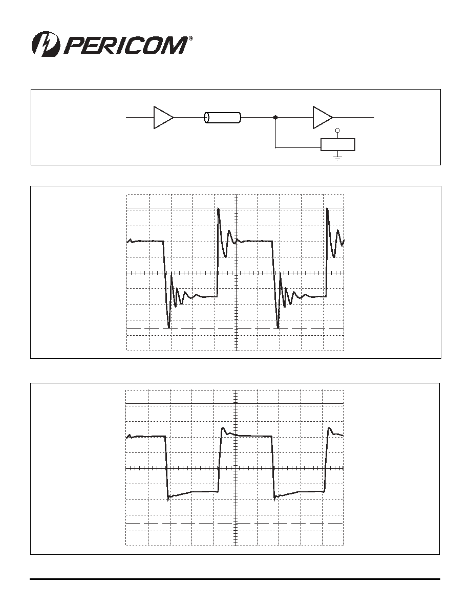
Application Information
Figure 2. VCX16244 (Vcc = 3.6V) output after driving 3-inch transmission line. Signal capture at end of line
Figure 1. Test Diagram
6.5V
3.5V
10ns/div.
6.5V
V
CC
= NC
V
CC
= 3.6V
3.5V
10ns/div.
Figure 3. VCX16244 (Vcc = 3.6V) output after driving 3-inch transmission line and driving PI7AT04 input.
Signal as seen at the input pin. Signal capture when Vcc in NC, Vcc = 3.6V.
PI7AT04
Transmission Line
Receiver
74VCX16244
Driver
74VCX16244
V
DD

4
PS8588C 08/02/04
12345678901234567890123456789012123456789012345678901234567890121234567890123456789012345678901212345678901234567890123456789012123456789012
12345678901234567890123456789012123456789012345678901234567890121234567890123456789012345678901212345678901234567890123456789012123456789012
PI7AT04
SOT
INYTM
Low Voltage, Zero-Delay,
Active Transmission Line Clamp
Ordering Code
Line Terminations
Package Code
Package Description
Top Marking
PI7AT04CX
4
C
6-pin SC70
Z9
PI7AT04CEX
4
C
6-pin SC70
Z9
Packaging Mechanical: 6-Pin SC70 (C)
5
6
4
2
1
3
Notes:
1) Controlling dimensions in millimeters
2) Ref: JEDEC MO-203AB
Ordering Information
Notes:
1. Thermal Characteristics can be found on the world wide web at www.pericom.com/packaging/
2. X = Tape and reel
Pericom Semiconductor Corporation ∑ 1-800-435-2336 ∑ www.pericom.com