Äîêóìåíòàöèÿ è îïèñàíèÿ www.docs.chipfind.ru

PI7C21P100
2-PORT PCI-X BRIDGE
REVISION 1.06
3545 NORTH FIRST STREET
SAN JOSE, CA 95134
PH: 1-877-PERICOM (1-877-737-4266)
FAX: 1-408-435-1100
EMAIL: SOLUTIONS@PERICOM.COM
INTERNET: HTTP://WWW.PERICOM.COM

LIFE SUPPORT POLICY
Pericom Semiconductor Corporation's products are not authorized for use as critical components in life
support devices or systems unless a specific written agreement pertaining to such intended use is executed
between the manufacturer and an officer of PSC.
1)
Life support devices or system are devices or systems which:
a)
Are intended for surgical implant into the body or
b)
Support or sustain life and whose failure to perform, when properly used in accordance with
instructions for use provided in the labeling, can be reasonably expected to result in a significant
injury to the user.
2)
A critical component is any component of a life support device or system whose failure to perform can
be reasonably expected to cause the failure of the life support device or system, or to affect its safety or
effectiveness. Pericom Semiconductor Corporation reserves the right to make changes to its products
or specifications at any time, without notice, in order to improve design or performance and to supply
the best possible product. Pericom Semiconductor does not assume any responsibility for use of any
circuitry described other than the circuitry embodied in a Pericom Semiconductor product. The
Company makes no representations that circuitry described herein is free from patent infringement or
other rights of third parties which may result from its use. No license is granted by implication or
otherwise under any patent, patent rights or other rights, of Pericom Semiconductor Corporation.
All other trademarks are of their respective companies.
PI7C21P100
2-PORT PCI-X BRIDGE
ADVANCE INFORMATION
Page 3 of 77
June 10, 2005 Revision 1.06
REVISION HISTORY
Date
Revision Number
Description
12/04/03
1.00
First Release of Data Sheet
12/11/03
1.01
Minor text corrections made.
01/22/04
1.02
Addition of Features section as well as a couple of tables.
Text corrections.
02/02/04
1.03
Corrected Device ID Register bits 11:0 descriptions.
03/15/04
1.04
Corrected pin designation for P_RST to E22 in section 3.2.1
09/13/04
1.05
Corrected Cin max in section 10.2 (DC specifications) from 0.8pF to
8pF
Added power consumption data in Section 10.4
04/13/05
1.051
Corrected pin description for TEST_CE0 (Y23) in section 3.2.8
06/10/05
1.06
Correct package outline drawing in section 11
Added Pb-free & Green ordering information in section 12

PI7C21P100
2-PORT PCI-X BRIDGE
ADVANCE INFORMATION
Page 4 of 77
June 10, 2005 Revision 1.06
This page intentionally left blank.

PI7C21P100
2-PORT PCI-X BRIDGE
ADVANCE INFORMATION
Page 5 of 77
June 10, 2005 Revision 1.06
TABLE OF CONTENTS
1
DESCRIPTION................................................................................................................................... 9
2
FEATURES ......................................................................................................................................... 9
3
SIGNAL DEFINITIONS.................................................................................................................. 10
3.1
SIGNAL
TYPES ....................................................................................................................... 10
3.2
SIGNALS .................................................................................................................................. 10
3.2.1
PRIMARY BUS INTERFACE SIGNALS............................................................................... 10
3.2.2
PRIMARY BUS INTERFACE SIGNALS 64-BIT EXTENSION.......................................... 12
3.2.3
SECONDARY BUS INTERFACE SIGNALS......................................................................... 13
3.2.4
SECONDARY BUS INTERFACE SIGNALS 64-BIT EXTENSION.................................... 14
3.2.5
CLOCK SIGNALS................................................................................................................. 15
3.2.6
STRAPPING PINS AND MISCELLANEOUS SIGNALS ...................................................... 16
3.2.7
JTAG BOUNDARY SCAN AND TEST SIGNALS ................................................................. 17
3.2.8
TEST SIGNALS..................................................................................................................... 18
3.2.9
POWER AND GROUND SIGNALS...................................................................................... 18
3.3
PIN
LIST ................................................................................................................................... 19
4
PCI BUS OPERATION.................................................................................................................... 22
4.1
TYPES
OF
TRANSACTIONS.................................................................................................. 22
4.2
WRITE
TRANSACTIONS ....................................................................................................... 23
4.2.1
MEMORY WRITE TRANSACTIONS .................................................................................... 23
4.2.1.1
PCI-X TO PCI-X ....................................................................................................................... 24
4.2.1.2
PCI TO PCI................................................................................................................................ 24
4.2.1.3
PCI TO PCI-X............................................................................................................................ 24
4.2.1.4
PCI-X TO PCI............................................................................................................................ 25
4.2.2
DELAYED/SPLIT WRITE TRANSACTIONS........................................................................ 25
4.2.3
IMMEDIATE WRITE TRANSACTIONS............................................................................... 25
4.3
READ
TRANSACTIONS......................................................................................................... 25
4.3.1
MEMORY READ TRANSACTIONS...................................................................................... 26
4.3.1.1
PCI-X TO PCI-X ....................................................................................................................... 26
4.3.1.2
PCI TO PCI................................................................................................................................ 26
4.3.1.3
PCI TO PCI-X............................................................................................................................ 26
4.3.1.4
PCI-X TO PCI............................................................................................................................ 27
4.3.2
I/O READ.............................................................................................................................. 27
4.3.3
CONFIGURATION READ ................................................................................................... 27
4.3.3.1
TYPE 1 CONFIGURATION READ ......................................................................................... 27
4.3.3.2
TYPE 0 CONFIGURATION READ ......................................................................................... 27
4.3.4
NON-PREFETCHABLE AND DWORD READS.................................................................. 28
4.3.5
PREFETCHABLE READS.................................................................................................... 28
4.3.5.1
PCI-X TO PCI-X AND PCI-X TO PCI .................................................................................... 28
4.3.5.2
PCI TO PCI................................................................................................................................ 28
4.3.5.3
PCI TO PCI-X............................................................................................................................ 29
4.3.6
DYNAMIC PREFETCH (CONVENTIONAL PCI MODE ONLY) ........................................ 29
4.4
CONFIGURATION
TRANSACTIONS ................................................................................... 29
4.4.1
TYPE 0 ACCESS TO PI7C21P100....................................................................................... 30
4.4.2
TYPE 1 TO TYPE 0 CONVERSION ..................................................................................... 30
4.4.3
TYPE 1 TO TYPE 1 FORWARDING.................................................................................... 31
4.4.4
SPECIAL CYCLES ............................................................................................................... 32
5
TRANSACTION ORDERING ........................................................................................................ 32
5.1
GENERAL
ORDERING
GUIDELINES................................................................................... 33
5.2
ORDERING
RULES................................................................................................................. 33
6
CLOCKS............................................................................................................................................ 34

PI7C21P100
2-PORT PCI-X BRIDGE
ADVANCE INFORMATION
Page 6 of 77
June 10, 2005 Revision 1.06
6.1
PRIMARY
AND
SECONDARY
CLOCK
INPUTS ................................................................. 34
6.2
CLOCK
JITTER........................................................................................................................ 34
6.3
MODE
AND
CLOCK
FREQUENCY
DETERMINATION ..................................................... 34
6.3.1
PRIMARY BUS ..................................................................................................................... 34
6.3.2
SECONDARY BUS ............................................................................................................... 35
6.3.3
CLOCK STABILITY.............................................................................................................. 36
6.3.4
DRIVER IMPEDANCE SELECTION................................................................................... 36
7
RESET ............................................................................................................................................... 36
7.1
PRIMARY
INTERFACE
RESET ............................................................................................. 37
7.2
SECONDARY
INTERFACE
RESET....................................................................................... 37
7.3
BUS
PARKING
&
BUS
WIDTH
DETERMINATION............................................................. 38
7.4
SECONDARY
DEVICE
MASKING........................................................................................ 38
7.5
ADDRESS
PARITY
ERRORS ................................................................................................. 39
7.6
OPTIONAL
BASE
ADDRESS
REGISTER ............................................................................. 39
7.7
OPTIONAL
CONFIGURATION
ACCESS
FROM
THE
SECONDARY
BUS........................ 39
7.8
SHORT
TERM
CACHING ....................................................................................................... 40
8
CONFIGURATION REGISTERS.................................................................................................. 41
8.1
CONFIGURATION
REGISTER
SPACE
MAP........................................................................ 41
8.1.1.1
SIGNAL TYPE DEFINITION................................................................................................... 42
8.1.2
VENDOR ID REGISTER OFFSET 00h............................................................................. 42
8.1.3
DEVICE ID REGISTER OFFSET 00h .............................................................................. 42
8.1.4
COMMAND REGISTER OFFSET 04h.............................................................................. 42
8.1.5
PRIMARY STATUS REGISTER OFFSET 04h .................................................................. 43
8.1.6
REVISION ID REGISTER OFFSET 08h ........................................................................... 44
8.1.7
CLASS CODE REGISTER OFFSET 08h........................................................................... 44
8.1.8
CACHE LINE SIZE REGISTER OFFSET 0Ch ................................................................. 44
8.1.9
PRIMARY LATENCY TIMER OFFSET 0Ch ..................................................................... 44
8.1.10
HEADER TYPE REGISTER OFFSET 0Ch................................................................... 44
8.1.11
BIST REGISTER OFFSET 0Ch .................................................................................... 44
8.1.12
LOWER MEMORY BASE ADDRESS REGISTER OFFSET 10h .................................. 45
8.1.13
UPPER MEMORY BASE ADDRESS REGISTER OFFSET 14h................................... 45
8.1.14
PRIMARY BUS NUMBER REGISTER OFFSET 18h ................................................... 45
8.1.15
SECONDARY BUS NUMBER REGISTER OFFSET 18h ............................................. 45
8.1.16
SUBORDINATE BUS NUMBER REGISTER OFFSET 18h ......................................... 45
8.1.17
SECONDARY LATENCY TIMER REGISTER OFFSET 18h ........................................ 45
8.1.18
I/O BASE ADDRESS REGISTER OFFSET 1Ch........................................................... 46
8.1.19
I/O LIMIT REGISTER OFFSET 1Ch............................................................................ 46
8.1.20
SECONDARY STATUS REGISTER OFFSET 1Ch ....................................................... 46
8.1.21
MEMORY BASE REGISTER OFFSET 20h .................................................................. 47
8.1.22
MEMORY LIMIT REGISTER OFFSET 20h ................................................................. 47
8.1.23
PREFETCHABLE MEMORY BASE REGISTER OFFSET 24h.................................... 47
8.1.24
PREFETCHABLE MEMORY LIMIT REGISTER OFFSET 24h................................... 47
8.1.25
PREFETCHABLE BASE UPPER 32-BIT REGISTER OFFSET 28h............................ 47
8.1.26
PREFETCHABLE LIMIT UPPER 32-BIT REGISTER OFFSET 2Ch.......................... 48
8.1.27
I/O BASE UPPER 16-BIT REGISTER OFFSET 30h.................................................... 48
8.1.28
I/O LIMIT UPPER 16-BIT REGISTER OFFSET 30h .................................................. 48
8.1.29
CAPABILITY POINTER OFFSET 34h ......................................................................... 48
8.1.30
EXPANSION ROM BASE ADDRESS REGISTER OFFSET 38h .................................. 48
8.1.31
INTERRUPT LINE REGISTER OFFSET 3Ch.............................................................. 48
8.1.32
INTERRUPT PIN REGISTER OFFSET 3Ch................................................................ 48
8.1.33
BRIDGE CONTROL REGISTER OFFSET 3Ch ........................................................... 49
8.1.34
PRIMARY DATA BUFFERING CONTROL REGISTER OFFSET 40h........................ 50
8.1.35
SECONDARY DATA BUFFERING CONTROL REGISTER OFFSET 40h.................. 51

PI7C21P100
2-PORT PCI-X BRIDGE
ADVANCE INFORMATION
Page 7 of 77
June 10, 2005 Revision 1.06
8.1.36
MISCELLANEOUS CONTROL REGISTER OFFSET 44h........................................... 52
8.1.37
EXTENDED CHIP CONTROL REGISTER 1 OFFSET 48h......................................... 52
8.1.38
EXTENDED CHIP CONTROL REGISTER 2 OFFSET 48h......................................... 53
8.1.39
ARBITER MODE REGISTER OFFSET 50h................................................................. 53
8.1.40
ARBITER ENABLE REGISTER OFFSET 54h.............................................................. 54
8.1.41
ARBITER PRIORITY REGISTER OFFSET 58h ........................................................... 54
8.1.42
SERR# DISABLE REGISTER OFFSET 5Ch ................................................................ 55
8.1.43
PRIMARY RETRY COUNTER REGISTER OFFSET 60h............................................. 56
8.1.44
SECONDARY RETRY COUNTER REGISTER OFFSET 64h....................................... 56
8.1.45
DISCARD TIMER CONTROL REGISTER OFFSET 68h............................................. 57
8.1.46
RETRY AND TIMER STATUS REGISTER OFFSET 6Ch ............................................ 57
8.1.47
OPAQUE MEMORY ENABLE REGISTER OFFSET 70h ............................................ 57
8.1.48
OPAQUE MEMORY BASE REGISTER OFFSET 74h ................................................. 58
8.1.49
OPAQUE MEMORY LIMIT REGISTER OFFSET 74h ................................................ 58
8.1.50
OPAQUE MEMORY BASE UPPER 32-BIT REGISTER OFFSET 78h ....................... 58
8.1.51
OPAQUE MEMORY LIMIT UPPER 32-BIT REGISTER OFFSET 7Ch...................... 58
8.1.52
PCI-X CAPABILITY ID REGISTER OFFSET 80h ....................................................... 58
8.1.53
NEXT CAPABILITY POINTER REGISTER OFFSET 80h ........................................... 59
8.1.54
PCI-X SECONDARY STATUS REGISTER OFFSET 80h............................................. 59
8.1.55
PCI-X BRIDGE PRIMARY STATUS REGISTER OFFSET 84h ................................... 59
8.1.56
SECONDARY BUS UPSTREAM SPLIT TRANSACTION REGISTER OFFSET 88h ... 61
8.1.57
PRIMARY BUS DOWNSTREAM SPLIT TRANSACTION REGISTER OFFSET 8Ch .. 61
8.1.58
POWER MANAGEMENT ID REGISTER OFFSET 90h............................................... 61
8.1.59
NEXT CAPABILITIES POINTER REGISTER OFFSET 90h........................................ 62
8.1.60
POWER MANAGEMENT CAPABILITIES REGISTER OFFSET 90h.......................... 62
8.1.61
POWER MANAGEMENT CONTROL AND STATUS REGISTER OFFSET 94h ......... 62
8.1.62
PCI-TO-PCI BRIDGE SUPPORT EXTENSION REGISTER OFFSET 94h ................. 63
8.1.63
SECONDARY BUS PRIVATE DEVICE MASK REGISTER OFFSET B0h................... 63
8.1.64
MISCELLANEOUS CONTROL REGISTER 2 OFFSET B8h ....................................... 64
9
IEEE 1149.1 COMPATIBLE JTAG CONTROLLER .................................................................. 65
9.1
INSTRUCTION
REGISTER..................................................................................................... 65
9.2
BYPASS
REGISTER ................................................................................................................ 65
9.3
DEVICE
ID
REGISTER ........................................................................................................... 65
9.4
BOUNDARY
SCAN
REGISTER ............................................................................................. 66
9.5
JTAG
BOUNDARY
REGISTER
ORDER................................................................................ 66
10
ELECTRICAL INFORMATION.................................................................................................... 74
10.1
MAXIMUM
RATINGS ............................................................................................................ 74
10.2
DC
SPECIFICATIONS............................................................................................................. 74
10.3
AC
SPECIFICATIONS............................................................................................................. 74
10.4
POWER
CONSUMPTION ....................................................................................................... 75
11
MECHANICAL INFORMATION.................................................................................................. 76
12
ORDERING INFORMATION........................................................................................................ 76

PI7C21P100
2-PORT PCI-X BRIDGE
ADVANCE INFORMATION
Page 8 of 77
June 10, 2005 Revision 1.06
LIST OF TABLES
T
ABLE
3-1
PIN
LIST
304-PIN
PBGA........................................................................................................... 19
T
ABLE
4-1
PCI
AND
PCI-X
TRANSACTIONS .......................................................................................... 22
T
ABLE
4-2
WRITE
TRANSACTION
FORWARDING ............................................................................... 23
T
ABLE
4-3
READ
TRANSACTIN
HANDLING.......................................................................................... 25
T
ABLE
4-4
DEVICE
NUMBER
TO
IDSEL.................................................................................................. 31
T
ABLE
5-1
SUMMARY
OF
TRANSACTION
ORDERING
IN
PCI
MODE ............................................... 33
T
ABLE
5-2
SUMMARY
OF
TRANSACTION
ORDERING
IN
PCI-X
MODE ........................................... 33
T
ABLE
6-1
PROGRAMMABLE
PULL-UP
CIRCUIT................................................................................. 35
T
ABLE
6-2
DRIVER
IMPEDANCE
SELECTION ....................................................................................... 36
T
ABLE
7-1
DELAY
TIMES
FOR
DE-ASSERTION
OF
S_RST# ................................................................ 38
T
ABLE
7-2
DE-ASSERTION
OF
S_RST#.................................................................................................... 38
T
ABLE
8-1
CONFIGURATION
SPACE
MAP ............................................................................................. 41
T
ABLE
9-1
JTAG
BOUNDARY
SCAN
REGISTER .................................................................................... 66
T
ABLE
10-1
AC
TIMING
SPECIFICATIONS
PCI-X
MODE...................................................................... 75
T
ABLE
10-2
AC
TIMING
SPECIFICATIONS
CONVENTIONAL
PCI
MODE.......................................... 75
LIST OF FIGURES
F
IGURE
10-1
PCI
SIGNAL
TIMING
MEASUREMENTS ........................................................................... 74
F
IGURE
11-1
PACKAGE
DIAGRAM
31
X
31
MM
304-PIN
HPBGA ........................................................... 76

PI7C21P100
2-PORT PCI-X BRIDGE
ADVANCE INFORMATION
Page 9 of 77
June 10, 2005 Revision 1.06
1
DESCRIPTION
The PI7C21P100 is a 2-port PCI-X 2.0 Bridge designed to be compliant with the PCI-X
Addendum to the Local Bus Specification Revision 1.0a. The PI7C21P100 is able to handle
64-bit data at a maximum bus frequency of 133MHz. The PI7C21P100 is designed for high
speed applications such as Ethernet, SCSI, and Fibre Channel. The PI7C21P100 may also be
used for bus expansion, frequency isolations/translations, or PCI-X to PCI
isolations/translations.
2
FEATURES
-
INDUSTRY STANDARDS COMPLIANCE
PCI-X Addendum to the Local Bus Specification Revision 1.0a (Mode 1 only)
PCI Local Bus Specification Revision 2.2
PCI-to-PCI Bridge Architecture Specification Revision 1.1
PCI Power Management Interface Specification Revision 1.1
·
Supports D0 and D3 power states
-
INTERFACE
3.3V signaling with 5V tolerance
133MHz / 64-bit operation on both buses
Dual address cycle support
Concurrent primary and secondary bus operation
Primary and secondary may be run in either PCI mode or PCI-X Mode 1
Asynchronous operation support
Programmable internal arbiter with support for up to 6 external masters on the
secondary bus
·
Internal arbiter may be disabled to use an external arbiter
IEEE 1149.1 JTAG support
-
OPERATION
Type 0 and Type 1 configuration support
Configuration register access from both primary and secondary buses
2KB of buffering for upstream memory burst read commands
2KB of buffering for downstream memory burst read commands
1KB of buffering for upstream posted memory write commands
1KB of buffering for downstream posted memory write commands
Support for up to 8 active transactions in each direction
-
ADDITIONAL FEATURES
Capabilities pointer
Ability to define an opaque memory address
Definable base address register
Secondary side PCI-X device privatization
-
PACKAGING
304-pin PBGA, 31 x 31 mm
PI7C21P100
2-PORT PCI-X BRIDGE
ADVANCE INFORMATION
Page 10 of 77
June 10, 2005 Revision 1.06
3
SIGNAL DEFINITIONS
3.1
SIGNAL TYPES
Signal Type
Description
I Input
Only
O Output
Only
P Power
TS Tri-State
bi-directional
STS
Sustained Tri-State. Active LOW signal must be pulled HIGH for 1 cycle when
deasserting.
OD Open
Drain
IU
Internal pull-up on signal
ID
Internal pull-down on signal
3.2
SIGNALS
Signal names that end with "#" are active LOW.
3.2.1
PRIMARY BUS INTERFACE SIGNALS
Name Pin
#
Type
Description
P_AD[31:0]
J23, M21, M22, L21,
L22, G23, K20, E23,
K21, D23, K22, J21,
J22, H21, H22, G21,
B20, G22, F20, F22,
D18, C19, C17, B17,
A20, C16, B16, A19,
C15, B14, C13, B13
TS
Primary Address / Data: Multiplexed address and data
bus. Address is indicated by P_FRAME# assertion.
Write data is stable and valid when P_IRDY# is asserted
and read data is stable and valid when P_TRDY# is
asserted. Data is transferred on rising clock edges when
both P_IRDY# and P_TRDY# are asserted. During bus
idle, PI7C21P100 drives P_AD[31:0] to a valid logic
level when P_GNT# is asserted.
P_CBE[3:0]#
A15, D14, B18, A13
TS
Primary Command/Byte Enables: Multiplexed
command field and byte enable field. During address
phase, the initiator drives the transaction type on these
pins. After that, the initiator drives the byte enables
during data phases. During bus idle, PI7C21P100 drives
P_CBE[3:0]# to a valid logic level when P_GNT# is
asserted.
P_PAR C18
TS
Primary Parity. P_PAR is even parity of P_AD[31:0]
and P_CBE[3:0] (i.e. an even number of 1's). P_PAR is
valid and stable one cycle after the address phase
(indicated by assertion of P_FRAME#) for address
parity. For write data phases, P_PAR is valid one clock
after P_IRDY# is asserted. For read data phase, P_PAR
is valid one clock after P_TRDY# is asserted. Signal
P_PAR is tri-stated one cycle after the P_AD lines are
tri-stated. During bus idle, PI7C21P100 drives P_PAR
to a valid logic level when P_GNT# is asserted.
P_FRAME# A17
STS
Primary FRAME (Active LOW). Driven by the
initiator of a transaction to indicate the beginning and
duration of an access. The de-assertion of P_FRAME#
indicates the final data phase requested by the initiator.
Before being tri-stated, it is driven HIGH for one cycle.
P_IRDY# A16
STS
Primary IRDY (Active LOW). Driven by the initiator
of a transaction to indicate its ability to complete current
data phase on the primary side. Once asserted in a data
phase, it is not de-asserted until the end of the data
phase. Before tri-stated, it is driven HIGH for one cycle.

PI7C21P100
2-PORT PCI-X BRIDGE
ADVANCE INFORMATION
Page 11 of 77
June 10, 2005 Revision 1.06
Name Pin
#
Type
Description
P_TRDY# B15
STS
Primary TRDY (Active LOW). Driven by the target of
a transaction to indicate its ability to complete current
data phase on the primary side. Once asserted in a data
phase, it is not de-asserted until the end of the data
phase. Before tri-stated, it is driven HIGH for one cycle.
P_DEVSEL# D21
STS
Primary Device Select (Active LOW). Asserted by the
target indicating that the device is accepting the
transaction. As a master, PI7C21P100 waits for the
assertion of this signal within 5 cycles of P_FRAME#
assertion; otherwise, terminate with master abort. Before
tri-stated, it is driven HIGH for one cycle.
P_STOP# C4
STS
Primary STOP (Active LOW). Asserted by the target
indicating that the target is requesting the initiator to stop
the current transaction. Before tri-stated, it is driven
HIGH for one cycle.
P_LOCK# C14
I
Primary LOCK (Active LOW). Asserted by an
initiator, one clock cycle after the first address phase of a
transaction, attempting to perform an operation that may
take more than one PCI transaction to complete.
P_IDSEL B19
I
Primary ID Select. Used as a chip select line for Type
0 configuration access to PI721P100 configuration
space.
P_PERR# C8
STS
Primary Parity Error (Active LOW). Asserted when
a data parity error is detected for data received on the
primary interface. Before being tri-stated, it is driven
HIGH for one cycle.
P_SERR# B4
OD
Primary System Error (Active LOW). Can be driven
LOW by any device to indicate a system error condition.
PI7C21P100 drives this pin on:
Address parity error
Posted write data parity error on target bus
Secondary S_SERR# asserted
Master abort during posted write transaction
Target abort during posted write transaction
Posted write transaction discarded
Delayed write request discarded
Delayed read request discarded
Delayed transaction master timeout
This signal requires an external pull-up resistor for
proper operation.
P_REQ# B21
TS
Primary Request (Active LOW): This is asserted by
PI7C21P100 to indicate that it wants to start a
transaction on the primary bus. PI7C21P100 de-asserts
this pin for at least 2 PCI clock cycles before asserting it
again.
P_GNT# C20
I
Primary Grant (Active LOW): When asserted,
PI7C21P100 can access the primary bus. During idle
and P_GNT# asserted, PI7C21P100 will drive P_AD,
P_CBE, and P_PAR to valid logic levels.
P_RST# E22
I
Primary RESET (Active LOW): When P_RESET# is
active, all PCI signals should be asynchronously tri-
stated.

PI7C21P100
2-PORT PCI-X BRIDGE
ADVANCE INFORMATION
Page 12 of 77
June 10, 2005 Revision 1.06
3.2.2
PRIMARY BUS INTERFACE SIGNALS 64-BIT EXTENSION
Name Pin
#
Type
Description
P_AD[63:32]
B11, D10, C10, A4,
B10, C9, B9, A3, B8,
B3, C7, B7, D6, B6,
B5, C2, D2, F4, E3,
F3, B1, F2, G3, H3,
H2, E1, J3, G1, H1,
J2, J1, L1
TS
Primary Upper 32-bit Address / Data: Multiplexed
address and data bus providing an additional 32 bits to
the primary. When a dual address command is used and
P_REQ64# is asserted, the initiator drives the upper 32
bits of the 64-bit address. Otherwise, these bits are
undefined and driven to valid logic levels. During the
data phase of a transaction, the initiator drives the upper
32 bits of the 64-bit write data, or the target drives the
upper 32 bits of the 64-bit read data, when P_REQ64#
and P_ACK64# are both asserted. Otherwise, these bits
are pulled up to a valid logic level through external
resistors.
P_CBE[7:4]#
A7, B12, C11, A5
TS
Primary Upper 32-bit Command/Byte Enables:
Multiplexed command field and byte enable field.
During address phase, when the dual address command
is used and P_REQ64# is asserted, the initiator drives the
transaction type on these pins. Otherwise, these bits are
undefined, and the initiator drives a valid logic level onto
the pins. For read and write transactions, the initiator
drives these bits for the P_AD[63:32] data bits when
P_REQ64# and P_ACK64# are both asserted. When not
driven, these bits are pulled up to a valid logic level
through external resistors.
P_PAR64 A9
TS
Primary Upper 32-bit Parity: P_PAR64 carries the
even parity of P_AD[63:32] and P_CBE[7:4] for both
address and data phases. P_PAR64 is driven by the
initiator and is valid 1 cycle after the first address phase
when a dual address command is used and P_REQ64# is
asserted. P_PAR64 is valid 1 clock cycle after the
second address phase of a dual address transaction when
P_REQ64# is asserted. P_PAR64 is valid 1 cycle after
valid data is driven when both P_REQ64# and
P_ACK64# are asserted for that data phase. P_PAR64 is
driven by the device driving read or write data 1 cycle
after the P_AD lines are driven. P_PAR64 is tri-stated 1
cycle after the P_AD lines are tri-stated. Devices receive
data sample P_PAR64 as an input to check for possible
parity errors during 64-bit transactions. When not driven,
P_PAR64 is pulled up to a valid logic level through
external resistors.
P_REQ64# C12
STS
Primary 64-bit Transfer Request: P_REQ64# is
asserted by the initiator to indicate that the initiator is
requesting a 64-bit data transfer. P_REQ64# has the
same timing as P_FRAME#. When P_REQ64# is
asserted LOW during reset, a 64-bit data path is
supported. When P_REQ64# is HIGH during reset,
PI7C21P100 drives P_AD[63:32], P_CBE[7:4], and
P_PAR64 to valid logic levels. When deasserting,
P_REQ64# is driven HIGH for 1 cycle and then
sustained by an external pull-up resistor.
P_ACK64# A2
STS
Primary 64-bit Transfer Acknowledge: P_ACK64# is
asserted by the target only when P_REQ64# is asserted
by the initiator to indicate the target's ability to transfer
data using 64 bits. P_ACK64# has the same timing as
P_DEVSEL#. When deasserting, P_ACK64# is driven
HIGH for 1 cycle and then is sustained by an external
pull-up resistor.

PI7C21P100
2-PORT PCI-X BRIDGE
ADVANCE INFORMATION
Page 13 of 77
June 10, 2005 Revision 1.06
3.2.3
SECONDARY BUS INTERFACE SIGNALS
Name Pin
#
Type
Description
S_AD[31:0]
N22, N21, P22, P21,
M23, P20, N23, R22,
T23, R21, W23, T22,
U22, U21, V22, V21,
W21, V20, AA20,
AB18, Y18, AA16,
AB15, AC17, AA13,
AA12, AC15, AB11,
AC11, AC9, AB9,
AA9
TS
Secondary Address/Data: Multiplexed address and data
bus. Address is indicated by S_FRAME# assertion.
Write data is stable and valid when S_IRDY# is asserted
and read data is stable and valid when S_IRDY# is
asserted. Data is transferred on rising clock edges when
both S_IRDY# and S_TRDY# are asserted. During bus
idle, PI7C21P100 drives S_AD[31:0] to a valid logic
level when the bridge is granted the bus.
S_CBE[3:0]#
AA15, AB14, AB16,
AB12
TS
Secondary Command/Byte Enables: Multiplexed
command field and byte enable field. During address
phase, the initiator drives the transaction type on these
pins. The initiator then drives the byte enables during
data phases. During bus idle, PI7C21P100 drives
S_CBE[3:0] to a valid logic level when the bridge is
granted the bus.
S_PAR AA17
TS
Secondary Parity: S_PAR is an even parity of
S_AD[31:0] and S_CBE[3:0] (i.e. an even number of
1's). S_PAR is valid and stable one cycle after the
address phase (indicated by assertion of S_FRAME#) for
address parity. For write data phases, S_PAR is valid
one clock after S_IRDY# is asserted. For read data
phase, S_PAR is valid one clock after S_TRDY# is
asserted. Signal S_PAR is tri-stated one cycle after the
S_AD lines are tri-stated. During bus idle, PI7C21P100
drives S_PAR to a valid logic level when the bridge is
granted the bus.
S_FRAME# AA14
STS
Secondary FRAME (Active LOW): Driven by the
initiator of a transaction to indicate the beginning and
duration of an access. The de-assertion of S_FRAME#
indicates the final data phase requested by the initiator.
Before being tri-stated, it is driven HIGH for one cycle.
S_IRDY# AC19
STS
Secondary IRDY (Active LOW): Driven by the
initiator of a transaction to indicate its ability to
complete current data phase on the secondary side. Once
asserted in a data phase, it is not de-asserted until the end
of the data phase. Before tri-stated, it is driven HIGH
for one cycle.
S_TRDY# Y14
STS
Secondary TRDY (Active LOW): Driven by the target
of a transaction to indicate its ability to complete current
data phase on the secondary side. Once asserted in a
data phase, it is not de-asserted until the end of the data
phase. Before tri-stated, it is driven HIGH for one cycle.
S_DEVSEL# AC21
STS
Secondary Device Select (Active LOW): Asserted by
the target indicating that the device is accepting the
transaction. As a master, PI7C21P100 waits for the
assertion of this signal within 5 cycles of S_FRAME#
assertion; otherwise, terminate with master abort. Before
tri-stated, it is driven HIGH for one cycle.
S_STOP# AB20
STS
Secondary STOP (Active LOW): Asserted by the
target indicating that the target is requesting the initiator
to stop the current transaction. Before tri-stated, it is
driven HIGH for one cycle.
S_LOCK# AC20
STS
Secondary LOCK (Active LOW): Asserted by an
initiator, one clock cycle after the first address phase of a
transaction, when it is propagating a locked transaction
downstream. PI7C21P100 does not propagate locked
transactions upstream.
S_PERR# AB17
STS
Secondary Parity Error (Active LOW): Asserted
when a data parity error is detected for data received on
the secondary interface. Before being tri-stated, it is
driven HIGH for one cycle.

PI7C21P100
2-PORT PCI-X BRIDGE
ADVANCE INFORMATION
Page 14 of 77
June 10, 2005 Revision 1.06
Name Pin
#
Type
Description
S_SERR# AB19
I
Secondary System Error (Active LOW): Can be
driven LOW by any device to indicate a system error
condition.
S_REQ[6:2]#
AC3, AB5, AB3,
W2, AA2
I
Secondary Request (Active LOW): This is asserted by
an external device to indicate that it wants to start a
transaction on the secondary bus. The input is externally
pulled up through a resistor to VDD.
S_REQ[1]# AA23
I
Secondary Request (Active LOW):
When the internal arbiter is enabled, this is asserted by
an external device to indicate that it wants to start a
transaction on the secondary bus. The input is externally
pulled up through a resistor to VDD.
When the internal arbiter is disabled, this is used by
PI7C21P100 as its GNT input.
S_GNT[6:2]#
AC4, AB4, AC5, Y2,
AB1
TS
Secondary Grant (Active LOW): PI7C21P100 asserts
these pins to allow external masters to access the
secondary bus. PI7C21P100 de-asserts these pins for at
least 2 PCI clock cycles before asserting it again.
During idle and S_GNT# deasserted, PI7C21P100 will
drive S_AD, S_CBE, and S_PAR.
S_GNT[1]# AA19
TS
Secondary Grant (Active LOW):
When the internal arbiter is enabled, PI7C21P100 asserts
this pin to allow external masters to access the
secondary bus. PI7C21P100 de-asserts this pin for at
least 2 PCI clock cycles before asserting it again.
During idle and S_GNT# deasserted, PI7C21P100 will
drive S_AD, S_CBE, and S_PAR.
When the internal arbiter is disabled, this is used by
PI7C21P100 as its REQ output.
S_RST# U23
O
Secondary RESET (Active LOW): Asserted when any
of the following conditions are met:
1.
Signal P_RESET# is asserted.
2.
Secondary reset bit in bridge control register in
configuration space is set.
3.
The chip reset bit in the chip control register in
configuration space is set.
When asserted, all control signals are tri-stated and
zeroes are driven on S_AD, S_CBE, S_PAR, and
S_PAR64.
3.2.4
SECONDARY BUS INTERFACE SIGNALS 64-BIT EXTENSION
Name Pin
#
Type
Description
S_AD[63:32]
AB8, AB7, AA7,
AB6, AA6, AA5, Y6,
Y3, V2, V4, U2, U3,
T2, T3, R2, R3, P2,
Y1, P3, W1, P4, U1,
N2, N3, M2, M3, R1,
L2, L3, K2, K3, K4
TS
Secondary Upper 32-bit Address/Data: Multiplexed
address and data bus. Address is indicated by
S_FRAME# assertion. Write data is stable and valid
when S_IRDY# is asserted and read data is stable and
valid when S_IRDY# is asserted. Data is transferred on
rising clock edges when both S_IRDY# and S_TRDY#
are asserted. During bus idle, PI7C21P100 drives S_AD
to a valid logic level when the bridge is granted the bus.
S_CBE[7:4]#
Y10, AB10, AA11,
AC8
TS
Secondary Upper 32-bit Command/Byte Enables:
Multiplexed command field and byte enable field.
During address phase, the initiator drives the transaction
type on these pins. The initiator then drives the byte
enables during data phases. During bus idle,
PI7C21P100 drives S_CBE[7:0] to a valid logic level
when the bridge is granted the bus.

PI7C21P100
2-PORT PCI-X BRIDGE
ADVANCE INFORMATION
Page 15 of 77
June 10, 2005 Revision 1.06
Name Pin
#
Type
Description
S_PAR64 AA10
TS
Secondary Upper 32-bit Parity: S_PAR64 carries the
even parity of S_AD[63:32] and S_CBE[7:4] for both
address and data phases. S_PAR64 is driven by the
initiator and is valid 1 cycle after the first address phase
when a dual address command is used and S_REQ64# is
asserted. S_PAR64 is valid 1 clock cycle after the
second address phase of a dual address transaction when
S_REQ64# is asserted. S_PAR64 is valid 1 cycle after
valid data is driven when both S_REQ64# and
S_ACK64# are asserted for that data phase. S_PAR64 is
driven by the device driving read or write data 1 cycle
after the S_AD lines are driven. S_PAR64 is tri-stated 1
cycle after the S_AD lines are tri-stated. Devices receive
data sample S_PAR64 as an input to check for possible
parity errors during 64-bit transactions. When not driven,
S_PAR64 is pulled up to a valid logic level through
external resistors.
S_REQ64# AB13
STS
Secondary 64-bit Transfer Request: S_REQ64# is
asserted by the initiator to indicate that the initiator is
requesting a 64-bit data transfer. S_REQ64# has the
same timing as S_FRAME#. When S_REQ64# is
asserted LOW during reset, a 64-bit data path is
supported. When S_REQ64# is HIGH during reset,
PI7C21P100 drives S_AD[63:32], S_CBE[7:4], and
S_PAR64 to valid logic levels. When deasserting,
S_REQ64# is driven to a deasserted state for 1 cycle and
then sustained by an external pull-up resistor.
S_ACK64# AA8
STS
Secondary 64-bit Transfer Acknowledge: S_ACK64#
is asserted by the target only when S_REQ64# is
asserted by the initiator to indicate the target's ability to
transfer data using 64 bits. S_ACK64# has the same
timing as S_DEVSEL#. When deasserting, S_ACK64#
is driven to a deasserted state for 1 cycle and then is
sustained by an external pull-up resistor.
3.2.5
CLOCK SIGNALS
Name Pin
#
Type
Description
P_CLK E21
I
Primary Clock Input: Provides timing for all
transactions on the primary interface. For conventional
PCI mode, the input clock frequency may be between 0
66MHz. In PCI-X mode, the input clock frequency
may be between 66 133MHz. See Section 6 for
limitations.
S_CLK AB23
I
Secondary Clock Input: Provides timing for all
transactions on the secondary interface. For conventional
PCI mode, the input clock frequency may be between 0
66MHz. In PCI-X mode, the input clock frequency
may be between 66 133MHz. See Section 6 for
limitations. If the primary bus is running at 133MHz,
the minimum frequency that may be supplied to S_CLK
is 33MHz.

PI7C21P100
2-PORT PCI-X BRIDGE
ADVANCE INFORMATION
Page 16 of 77
June 10, 2005 Revision 1.06
3.2.6
STRAPPING PINS AND MISCELLANEOUS SIGNALS
Name Pin
#
Type
Description
S__ARB# T21
I
Internal Arbiter Enable: This pin is used by
PI7C21P100 to determine whether the secondary bus
uses the internal arbiter or external arbiter.
0: Enable the internal arbiter
1: Disable the internal arbiter and use an external arbiter
S_SEL100 V3
I
Secondary Bus Maximum Frequency: This pin is used
to determine the maximum frequency on the secondary
bus when in PCI-X mode. In PCI mode, the pin has no
function and should not be left floating.
0: Set secondary interface to 133MHz
1: Set secondary interface to 100MHz
S_PCIXCAP R23
I
Secondary Bus PCI-X Capable: This pin is used with
S_SEL100 to determine the frequency and mode for the
secondary bus. There are three conditions for this pin
determining the capability of the secondary bus:
Ground: Not capable of PCI-X mode
Pull-down: PCI-X 66MHz
Not connected: PCI-X 133MHz
S_PCIXCAP_PU AA1
I S_PCIXCAP Pull-up Driver: This pin is used with
S_PCIXAP as part of a programmable pull-up circuit to
determine the state of S_PCIXCAP. A 1kohm resistor
must be placed between this pin and S_PCIXCAP.
S_DRVR AC7
ID
Secondary Driver Mode: This pin controls the output
impedance of the secondary drivers to account for the
number of loads on the secondary bus.
0: default impedance
1: select alternate impedance
See Table 6-2 for impedance values.
P_DRVR E2
ID
Primary Driver Mode Control: Controls the output
impedance of the primary bus drivers to account for the
number of loads on the primary bus.
0: Default impedance
1: Select alternate impedance
S_CLK_STABLE W3
I S_CLK Input Stable: Determines when the S_CLK is
stable to resolve when S_RST# can by de-asserted.
0: S_CLK is not stable
1: S_CLK is stable
S_IDSEL AA22
I
Initialization Device Select: S_IDSEL is used as a chip
select during configuration reads and writes on the
secondary bus. Applications that do not require access
to PI7C21P100's configuration registers from the
secondary side should pull this pin LOW.

PI7C21P100
2-PORT PCI-X BRIDGE
ADVANCE INFORMATION
Page 17 of 77
June 10, 2005 Revision 1.06
64BIT_DEV# Y22
I
PCI-X Device Bus Width: 64BIT_DEV# sets bit 16 of
the PCI-X Bridge Status Register to support system
management software. This signal does not change the
behavior of the bridge.
0: Sets bit 16 of the PCI-X bridge status register to 1
1: Sets bit 16 of the PCI-X bridge status register to 0
BAR_EN G2
I
Base Address Register Enable: BAR_EN is used to
enable the base address at reset or power up. When
enabled, the 64-bit register at offset 10h and offset 14h is
used to claim a 1MB memory region.
0: Disabled register returns 0 and no memory region is
claimed
1: Enabled bits 63:20 can be written by software to
claim a 1MB memory region
IDSEL_ROUTE AC22
I IDSEL Reroute Enable: Controls the IDSEL reroute
function at reset or power up. The reset value of the
secondary bus private device mask register is changed
according to the value of this pin.
0: Reset value of the secondary bus private device mask
register is 00000000h
1: Reset value of the secondary bus private device mask
register is 22F20000h
OPAQUE_EN AA18
I Opaque Region Enable: Used to enable the opaque
memory region at reset or power up. Controls bit[0]
offset 70h.
0: Disable opaque memory address range
1: Enable opaque memory address range
P_CFG_BUSY C6
I Primary Configuration Busy: Determines the value of
bit [2] offset 44h to sequence initialization on the
primary and secondary buses for applications that
require bridge configuration from the secondary bus.
Applications that do not require configuration from the
secondary bus should pull this pin down to ground.
0: Type 0 configuration commands accepted normally on
the primary bus.
1: Type 0 configuration commands are retried on the
primary bus.
RESERVED D1
-
Reserved. Must be tied to ground.
3.2.7
JTAG BOUNDARY SCAN AND TEST SIGNALS
Name Pin
#
Type
Description
TCK F21
IU
Test Clock. Used to clock state information and data
into and out of the PI721P100 during boundary scan.
TMS D22
IU
Test Mode Select. Used to control the state of the Test
Access Port controller.
TDO B23
O
Test Data Output. Used as the serial output for the test
instructions and data from the test logic.
TDI C22
IU
Test Data Input. Serial input for the JTAG instructions
and test data.
TRST# C23
IU
Test Reset. Active LOW signal to reset the Test Access
Port (TAP) controller into an initialized state.
PI7C21P100
2-PORT PCI-X BRIDGE
ADVANCE INFORMATION
Page 18 of 77
June 10, 2005 Revision 1.06
3.2.8
TEST SIGNALS
Name Pin
#
Type
Description
T_DI1 Y21
IU
PLL Bypass Control for PCI-X Mode. The strapped
value of this pin (at P_RST# deassertion) controls
whether the internal PLL's are bypassed in PCI-X mode.
HIGH: PLL's are used in PCI-X mode
LOW: PLL's are bypassed in PCI-X mode
T_DI2 AA4
IU
Shorten Initialization Period. Controls the period for
the following signals during initialization.
LOW: Shorten periods
T
PIRSTDLY
- 5 Primary Clocks
T
XCAP
6 Primary Clocks
T
SIRSTDLY
- 40 Secondary Clocks
T
SRSTDLY
11 Secondary Clocks + 7 Primary Clocks
HIGH: Normal initialization
T
PIRSTDLY
See Table 7-2
T
XCAP
See Table 7-2
T
SIRSTDLY
See Table 7-2
T
SRSTDLY
See Table 7-2
T_MODECTL
T_RI
XCLK_OUT
C1
W22
D3
I
I
I
PLL Test Control. Controls along with the internal
PLL testing.
T_RI T_MODECTL XCLK_OUT
H L
Z
H H P_CLK*
L H
S_CLK**
* P_PLL enabled, S_PLL disabled
**P_PLL disabled, S_PLL enabled
T_RI W22
I
PLL Bypass Control for PCI Mode. The strapped
value of this pin (at T_RI) controls whether the internal
PLL's are bypassed in PCI mode.
1: PLL's are bypassed in PCI mode
0 and T_MODECTL=0: PLL's are used in PCI mode
TEST_CE0 Y23
ID
Reserved. Chip testing only. Tie LOW for normal
operation.
3.2.9
POWER AND GROUND SIGNALS
Name Pin
#
Type
Description
P_VDDA A21
P
2.5V Power: Power supply to the PLL for the primary
clock domain.
P_VSSA D16
P
2.5V Power: Ground for the PLL for the primary clock
domain.
S_VDDA AB21
P
2.5V Power: Power supply to the PLL for the secondary
clock domain.
S_VSSA Y16
P
2.5V Power: Ground for the PLL for the secondary
clock domain.
VDD
D9, D11, D13, D15,
J4, J20, L4, L20, N4,
N20, R4, R20, Y9,
Y11, Y13, Y15
P
2.5 Power: Power supply for the internal logic
PI7C21P100
2-PORT PCI-X BRIDGE
ADVANCE INFORMATION
Page 19 of 77
June 10, 2005 Revision 1.06
Name Pin
#
Type
Description
VDD2
A8, A12, A22, C5,
D5, D7, D17, D19,
E4, E20, G4, G20,
H23, M1, T1, U4,
U20, W4, W20, Y5,
Y7, Y17, Y19, AC2,
AC12, AC16
P
3.3 Power: Power supply for the I/O
VSS
A1, A6, A10, A11,
A14, A18, A23, B2,
B22, C3, C21, D4,
D8, D12, D20, F1,
F23, H4, H20, K1,
K23, L23, M4, M20,
N1, P1, P23, T4,
T20, V1, V23, Y4,
Y8, Y12, Y20, AA3,
AA21, AB2, AB22,
AC1, AC6, AC10,
AC13, AC14, AC18,
AC23
P
Ground
3.3
PIN LIST
Table 3-1 PIN LIST 304-PIN PBGA
BALL
LOCATION
PIN NAME
TYPE
BALL
LOCATION
PIN NAME
TYPE
A1 VSS P
A2 P_ACK64#
STS
A3 P_AD[56]
TS
A4 P_AD[60]
TS
A5 P_CBE[4]#
TS
A6 VSS P
A7 P_CBE[7]#
TS
A8 VDD2 P
A9 P_PAR64
TS
A10 VSS P
A11 VSS
P A12 VDD2 P
A13 P_CBE[0]#
TS
A14 VSS
P
A15 P_CBE[3]#
TS
A16 P_IRDY#
STS
A17 P_FRAME#
STS
A18 VSS
P
A19 P_AD[4] TS
A20 P_AD[7] TS
A21 P_VDDA
P A22 VDD2 P
A23 VSS
P B1 P_AD[43]
TS
B2 VSS P
B3 P_AD[54]
TS
B4 P_SERR#
OD
B5 P_AD[49]
TS
B6 P_AD[50]
TS
B7 P_AD[52]
TS
B8 P_AD[55]
TS
B9 P_AD[57]
TS
B10 P_AD[59]
TS
B11 P_AD[63]
TS
B12 P_CBE[6]#
TS
B13 P_AD[0] TS
B14 P_AD[2] TS
B15 P_TRDY#
STS
B16 P_AD[5] TS
B17 P_AD[8] TS
B18 P_CBE[1]#
TS
B19 P_IDSEL
I
B20 P_AD[15]
TS
B21 P_REQ# TS
B22 VSS
P B23 TDO
O
C1 T_MODECTL
I
C2 P_AD[48]
TS
C3 VSS P
C4 P_STOP#
STS
C5 VDD2 P
C6 P_CFG_BUSY
I
C7 P_AD[53]
TS
C8 P_PERR#
STS
C9 P_AD[58]
TS
C10 P_AD[61]
TS
C11 P_CBE[5]#
TS
C12 P_REQ64#
STS
C13 P_AD[1] TS
C14 P_LOCK#
I
C15 P_AD[3] TS
C16 P_AD[6] TS
C17 P_AD[9] TS
C18 P_PAR TS
C19 P_AD[10]
TS
C20 P_GNT# I
C21 VSS
P C22 TDI
I
C23 TRST# I D1 RESERVED
-

PI7C21P100
2-PORT PCI-X BRIDGE
ADVANCE INFORMATION
Page 20 of 77
June 10, 2005 Revision 1.06
BALL
LOCATION
PIN NAME
TYPE
BALL
LOCATION
PIN NAME
TYPE
D2 P_AD[47]
TS
D3 XCLK_OUT
I
D4 VSS P
D5 VDD2 P
D6 P_AD[51]
TS
D7 VDD2 P
D8 VSS P
D9 VDD P
D10 P_AD[62]
TS
D11 VDD P
D12 VSS
P D13 VDD P
D14 P_CBE[2]#
TS
D15 VDD P
D16 P_VSSA P D17 VDD2 P
D18 P_AD[11]
TS
D19 VDD2 P
D20 VSS
P D21 P_DEVSEL#
STS
D22 TMS
I D23 P_AD[22]
TS
E1 P_AD[38]
TS
E2 P_DRVER
I
E3 P_AD[45]
TS
E4 VDD2 P
E20 VDD2 P E21 P_CLK I
E22 P_RST# I E23 P_AD[24]
TS
F1 VSS P
F2 P_AD[42]
TS
F3 P_AD[44]
TS
F4 P_AD[46]
TS
F20 P_AD[13]
TS
F21 TCK I
F22 P_AD[12]
TS
F23 VSS
P
G1 P_AD[36]
TS
G2 BAR_EN
I
G3 P_AD[41]
TS
G4 VDD2 P
G20 VDD2 P G21 P_AD[16]
TS
G22 P_AD[14]
TS
G23 P_AD[26]
TS
H1 P_AD[35]
TS
H2 P_AD[39]
TS
H3 P_AD[40]
TS
H4 VSS P
H20 VSS
P H21 P_AD[18]
TS
H22 P_AD[17]
TS
H23 VDD2 P
J1 P_AD[33]
TS
J2 P_AD[34]
TS
J3 P_AD[37]
TS
J4 VDD P
J20 VDD P
J21 P_AD[20]
TS
J22 P_AD[19]
TS
J23 P_AD[31]
TS
K1 VSS P
K2 S_AD[34]
TS
K3 S_AD[33]
TS
K4 S_AD[32]
TS
K20 P_AD[25]
TS
K21 P_AD[23]
TS
K22 P_AD[21]
TS
K223 VSS
P
L1 P_AD[32]
TS
L2 S_AD[36]
TS
L3 S_AD[35]
TS
L4 VDD P
L20 VDD P L21 P_AD[28]
TS
L22 P_AD[27]
TS
L23 VSS
P
M1 VDD2 P
M2 S_AD[39]
TS
M3 S_AD[38]
TS
M4 VSS P
M20 VSS
P M21 P_AD[30]
TS
M22 P_AD[29]
TS
M23 S_AD[27]
TS
N1 VSS P
N2 S_AD[41]
TS
N3 S_AD[40]
TS
N4 VDD P
N20 VDD P N21 S_AD[30]
TS
N22 S_AD[31]
TS
N23 S_AD[25]
TS
P1 VSS P
P2 S_AD[47]
TS
P3 S_AD[45]
TS
P4 S_AD[43]
TS
P20 S_AD[26]
TS
P21 S_AD[28]
TS
P22 S_AD[29]
TS
P23 VSS
P
R1 S_AD[37]
TS
R2 S_AD[49]
TS
R3 S_AD[48]
TS
R4 VDD P
R20 VDD P R21 S_AD[22]
TS
R22 S_AD[24]
TS
R23 S_PCIXCAP
I
T1 VDD2 P
T2 S_AD[51]
TS
T3 S_AD[50]
TS
T4 VSS P
T20 VSS
P T21 S_ARB# I
T22 S_AD[20]
TS
T23 S_AD[23]
TS
U1 S_AD[42]
TS
U2 S_AD[53]
TS
U3 S_AD[52]
TS
U4 VDD2 P
U20 VDD2 P U21 S_AD[18]
TS
U22 S_AD[19]
TS
U23 S_RST# O

PI7C21P100
2-PORT PCI-X BRIDGE
ADVANCE INFORMATION
Page 21 of 77
June 10, 2005 Revision 1.06
BALL
LOCATION
PIN NAME
TYPE
BALL
LOCATION
PIN NAME
TYPE
V1 VSS P
V2 S_AD[55]
TS
V3 S_SEL100
I
V4 S_AD[54]
TS
V20 S_AD[14]
TS
V21 S_AD[16]
TS
V22 S_AD[17]
TS
V23 VSS
P
W1 S_AD[44]
TS
W2 S_REQ[3]#
I
W3 S_CLK_STABLE
I W4 VDD2 P
W20 VDD2 P W21 S_AD[15]
TS
W22 T_RI
I W23 S_AD[21]
TS
Y1 S_AD[46]
TS
Y2 S_GNT[3]#
TS
Y3 S_AD[56]
TS
Y4 VSS P
Y5 VDD2 P
Y6 S_AD[57]
TS
Y7 VDD2 P
Y8 VSS P
Y9 VDD P
Y10 S_CBE[7]#
TS
Y11 VDD P Y12 VSS
P
Y13 VDD P Y14 S_TRDY#
STS
Y15 VDD P Y16 S_VSSA P
Y17 VDD2 P Y18 S_AD[11]
TS
Y19 VDD2 P Y20 VSS
P
Y21 T_DI1 I Y22 64BIT_DEV#
I
Y23 TEST_CE0
I AA1 S_PCIXCAP_PU
I
AA2 S_REQ[2]#
I AA3 VSS
P
AA4 T_DI2 I AA5 S_AD[58]
TS
AA6 S_AD[59]
TS
AA7 S_AD[61]
TS
AA8 S_ACK64#
STS
AA9 S_AD[0] TS
AA10 S_PAR64 TS AA11 S_CBE[5]#
TS
AA12 S_AD[6] TS AA13 S_AD[7] TS
AA14 S_FRAME#
STS
AA15 S_CBE[3]#
TS
AA16 S_AD[10] TS AA17 S_PAR TS
AA18 OPAQUE_EN
I AA19 S_GNT[1]#
TS
AA20 S_AD[13] TS AA21 VSS
P
AA22 S_IDSEL I AA23 S_REQ[1]#
I
AB1 S_GNT[2]#
TS
AB2 VSS
P
AB3 S_REQ[4]#
I AB4 S_GNT[5]#
TS
AB5 S_REQ[5]#
I AB6 S_AD[60]
TS
AB7 S_AD[62]
TS
AB8 S_AD[63]
TS
AB9 S_AD[1] TS
AB10 S_CBE[6]#
TS
AB11 S_AD[4] TS AB12 S_CBE[0]#
TS
AB13 S_REQ64#
STS
AB14 S_CBE[2]#
TS
AB15 S_AD[9] TS AB16 S_CBE[1]#
TS
AB17 S_PERR# STS
AB18 S_AD[12] TS
AB19 S_SERR# I AB20 S_STOP# STS
AB21 S_VDDA P AB22 VSS
P
AB23 S_CLK I AC1 VSS
P
AC2 VDD2 P AC3 S_REQ[6]#
I
AC4 S_GNT[6]#
TS
AC5 S_GNT[4]#
TS
AC6 VSS
P AC7 S_DRVR I
AC8 S_CBE[4]#
TS
AC9 S_AD[2] TS
AC10 VSS
P AC11 S_AD[3] TS
AC12 VDD2
P AC13 VSS
P
AC14 VSS
P AC15 S_AD[5] TS
AC16 VDD2
P AC17 S_AD[8] TS
AC18 VSS
P AC19 S_IRDY# STS
AC20 S_LOCK# STS
AC21 S_DEVSEL#
STS
AC22 IDSEL_ROUTE
I AC23 VSS
P
PI7C21P100
2-PORT PCI-X BRIDGE
ADVANCE INFORMATION
Page 22 of 77
June 10, 2005 Revision 1.06
4
PCI BUS OPERATION
This Chapter offers information about PCI transactions, transaction forwarding across
PI7C21P100, and transaction termination. The PI7C21P100 has two 2KB buffers for read
data buffering of upstream and downstream transactions. Also, PI7C21P100 has two 1KB
buffers for write data buffering of upstream and downstream transactions.
4.1
TYPES OF TRANSACTIONS
This section provides a summary of PCI and PCI-X transactions performed by PI7C21P100.
Table 4-1 lists the command code and name of each PCI and PCI-X transaction. The Master
and Target columns indicate support for each transaction when PI7C21P100 initiates
transactions as a master, on the primary and secondary buses, and when PI7C21P100
responds to transactions as a target, on the primary and secondary buses.
Table 4-1 PCI AND PCI-X TRANSACTIONS
Types of Transactions
Initiates as Master
Responds as Target
Primary
Secondary
Primary
Secondary
0000 Interrupt
Acknowledge
N
N
N
N
0001 Special
Cycle
Y
Y
N
N
0010 I/O
Read
Y
Y
Y
Y
0011 I/O
Write
Y
Y
Y
Y
0100 Reserved
N
N
N
N
0101 Reserved
N
N
N
N
0110 Memory
Read
Y
Y
Y
Y
0111 Memory
Write
Y
Y
Y
Y
1000 Reserved
N
N
N
N
1001 Reserved
N
N
N
N
1010
Configuration Read
N
Y
Y
Y (Type 0 only)
1011
Configuration Write
Y (Type 1 only)
Y
Y
Y
1100
Memory Read Multiple
Y
Y
Y
Y
1101
Dual Address Cycle
Y
Y
Y
Y
1110
Memory Read Line
Y
Y
Y
Y
1111
Memory Write and Invalidate
Y
Y
Y
Y
As indicated in Table 4-1, the following commands are not supported by PI7C21P100:
PI7C21P100 never initiates a transaction with a reserved command code and, as a target,
PI7C21P100 ignores reserved command codes.
PI7C21P100 does not generate interrupt acknowledge transactions. PI7C21P100 ignores
interrupt acknowledge transactions as a target.
PI7C21P100 does not respond to special cycle transactions. PI7C21P100 cannot
guarantee delivery of a special cycle transaction to downstream buses because of the
broadcast nature of the special cycle command and the inability to control the transaction as a
target. To generate special cycle transactions on other buses, either upstream or downstream,
Type 1 configuration write must be used.
PI7C21P100
2-PORT PCI-X BRIDGE
ADVANCE INFORMATION
Page 23 of 77
June 10, 2005 Revision 1.06
4.2
WRITE TRANSACTIONS
Write transactions are treated as posted write, delayed/split (PCI-X), or immediate write
transactions. Table 4-2 shows the method of forwarding used for each type of write
operation.
Table 4-2 WRITE TRANSACTION FORWARDING
Type of Transaction
Type of Forwarding
Memory Write
Posted
Memory Write and Invalidate
Posted
Memory Write Block (PCI-X)
Posted
I/O Write
Delayed / Split (PCI-X)
Type 0 Configuration Write
Immediate on the primary bus.
Delayed / Split (PCI-X) on the secondary bus.
Type 1 Configuration Write
Delayed / Split (PCI-X)
4.2.1
MEMORY WRITE TRANSACTIONS
Posted write forwarding is used for "Memory Write", "Memory Write and Invalidate", and
"Memory Write Block" transactions.
When PI7C21P100 determines that a memory write transaction is to be forwarded across the
bridge, PI7C21P100 asserts DEVSEL# with medium decode timing and TRDY# in the next
cycle, provided that enough buffer space is available in the posted memory write queue for
the address and at least one DWORD of data. Under this condition, PI7C21P100 accepts write
data without obtaining access to the target bus. The PI7C21P100 can accept one DWORD of
write data every PCI clock cycle. That is, no target wait state is inserted. The write data is
stored in an internal posted write buffers and is subsequently delivered to the target. The
PI7C21P100 continues to accept write data until one of the following events occurs:
The initiator terminates the transaction by de-asserting FRAME# and IRDY#.
An internal write address boundary is reached, such as a cache line boundary or an
aligned 4KB boundary, depending on the transaction type.
The posted write data buffer fills up.
When one of the last two events occurs, the PI7C21P100 returns a target disconnect to the
requesting initiator on this data phase to terminate the transaction.
Once the posted write data moves to the head of the posted data queue, PI7C21P100 asserts
its request on the target bus. This can occur while PI7C21P100 is still receiving data on the
initiator bus. When the grant for the target bus is received and the target bus is detected in the
idle condition, PI7C21P100 asserts FRAME# and drives the stored write address out on the
target bus. On the following cycle, PI7C21P100 drives the first DWORD of write data and
continues to transfer write data until all write data corresponding to that transaction is
delivered, or until a target termination is received. As long as write data exists in the queue,
PI7C21P100 can drive one DWORD of write data in each PCI clock cycle; that is, no master
wait states are inserted. If write data is flowing through PI7C21P100 and the initiator stalls,
PI7C21P100 will signal the last data phase for the current transaction at the target bus if the
queue empties. PI7C21P100 will restart the follow-on transactions if the queue has new data.

PI7C21P100
2-PORT PCI-X BRIDGE
ADVANCE INFORMATION
Page 24 of 77
June 10, 2005 Revision 1.06
PI7C21P100 ends the transaction on the target bus when one of the following conditions is
met:
All posted write data has been delivered to the target.
The target returns a target disconnect or target retry (PI7C21P100 starts another
transaction to deliver the rest of the write data).
The target returns a target abort (PI7C21P100 discards remaining write data).
The master latency timer expires, and PI7C21P100 no longer has the target bus grant
(PI7C21P100 starts another transaction to deliver remaining write data).
4.2.1.1
PCI-X TO PCI-X
When both buses are operating in the PCI-X mode, PI7C21P100 passes the memory write
command that it receives to the destination interface along with the originating byte count and
transaction ID. PI7C21P100 attempts to transfer a memory write command when the
transaction ends or a 128-byte boundary is crossed. As long as there is at least 128-byte of
data in the data buffer or the end of transfer remains from the PCI-X memory write command
when a 128-byte boundary is crossed, the transfer will continue. If a transaction is
disconnected on the destination interface in the middle of a continuing transfer, the byte count
and address are updated and the transaction is presented again on the destination interface. If a
transaction is disconnected in the middle of a continuing transfer on the originating interface,
the originator must present the transaction again with the updated byte count and address.
4.2.1.2
PCI TO PCI
When both buses are operating in conventional PCI mode, the bridge passes the memory write
command that it receives to the destination interface, unless PI7C21P100 is disconnected in
the middle of a memory write and invalidate and is not on a cache line boundary. If this
happens, the command will continue as a memory write when PI7C21P100 attempts to
reconnect. PI7C21P100 attempts to transfer a memory write command when the transaction
ends or a 128-byte boundary is crossed. As long as a 128-byte buffer is full or the end of
transfer remains from the memory write command when a 128-byte boundary is crossed, the
transfer will continue.
4.2.1.3
PCI TO PCI-X
When the originating bus is operating in the conventional PCI mode and the destination bus is
operating in the PCI-X mode, PI7C21P100 must buffer memory write transactions from the
conventional PCI interface and count the number of bytes to be forwarded to the PCI-X
interface. If the conventional PCI transaction uses the memory write command and some byte
enables are not asserted, PI7C21P100 must use the PCI-X memory write command. If the
conventional PCI command is memory write and all byte enables are asserted, PI7C21P100
will use the PCI-X memory write command. If the conventional transaction uses the memory
write and invalidate command, PI7C21P100 uses the PCI-X memory write block command.
PI7C21P100 attempts to transfer the write data on the PCI-X interface as soon as the
transaction ends or a 128-byte boundary is crossed. Writes greater than 128 bytes are possible
only if more than one 128-byte sector fills up before the write operation is issued on the PCI-
X interface.
PI7C21P100
2-PORT PCI-X BRIDGE
ADVANCE INFORMATION
Page 25 of 77
June 10, 2005 Revision 1.06
4.2.1.4
PCI-X TO PCI
When the originating bus is operating in the PCI-X mode and the destination bus is operating
in the conventional PCI mode, PI7C21P100 uses the PCI conventional memory write
command for both the PCI-X memory write and PCI-X memory write block commands.
PI7C21P100 attempts to transfer write data on the conventional PCI interface when the PCI-X
data crosses a 128-byte boundary or the end of the PCI-X transfer occurs. As long as a 128-
byte buffer is full, or the end of transfer remains from the PCI-X memory write command
when a 128-byte boundary is crossed, the transfer will continue on the conventional PCI
interface.
4.2.2
DELAYED/SPLIT WRITE TRANSACTIONS
Delayed/Split write forwarding is used for I/O write transactions, Type 1 configuration write
transactions, and Type 0 configuration write transactions.
Delayed/Split write forwarding transactions are retried on the originating bus, completed on
the destination bus (if necessary), and then completed on the originating bus. For DWORD
transactions, PI7C21P100 uses delayed transactions in conventional PCI mode and split
requests in PCI-X mode. Only one request queue entry is allowed for either delayed or split
write transactions.
4.2.3
IMMEDIATE WRITE TRANSACTIONS
PI7C21P100 considers Type 0 configuration writes on the primary bus meant for the bridge as
immediate write transactions for the bridge. PI7C21P100 will execute the transaction and
indicate its completion by accepting the DWORD of data immediately.
4.3
READ TRANSACTIONS
Read transactions are treated as delayed read for conventional PCI mode, split read for PCI-X
mode, or immediate read. Table 4-3 shows the read behavior.
Table 4-3 READ TRANSACTIN HANDLING
Type of Transaction
Type of Handling
Memory Read
Delayed
Memory Read Line
Delayed
Memory Read Multiple
Delayed
Memory Read DWORD (PCI-X mode)
Split (PCI-X mode)
Memory Read Block (PCI-X mode)
Split (PCI-X mode)
I/O Read
Delayed/Split (PCI-X)
Type 0 Configuration Read
Immediate on the primary bus, Delayed/Split (PCI-X
mode) on the secondary bus
Type 1 Configuration Read
Delayed/Split (PCI-X mode)

PI7C21P100
2-PORT PCI-X BRIDGE
ADVANCE INFORMATION
Page 26 of 77
June 10, 2005 Revision 1.06
4.3.1
MEMORY READ TRANSACTIONS
Memory data is transferred from the originating side of PI7C21P100 to the destination side
using PCI memory read, memory read line, memory read multiple, PCI-X memory read
DWORD, and PCI-X memory read block transactions. All memory read transactions are
either delayed or split on the originating side of PI7C21P100 depending on the mode of the
originating side.
4.3.1.1
PCI-X TO PCI-X
No translation is needed for these transactions.
The amount of data that is fetched is controlled by the downstream and upstream split
transaction control register. The split transaction capacity and split transaction commitment
limit fields control how much data is requested at any one time.
4.3.1.2
PCI TO PCI
No translation is needed for these transactions.
Memory Read Fetches only the requested DWORD if the command targets a non-
prefetchable memory space. Bits [25:24] offset 40h and bits [9:8] offset 40h control the mode
of prefetching for memory read transactions in the prefetchable range on the secondary and
primary bus respectively. The default is up to one cache line will be prefetched.
Memory Read Line Bits [23:22] offset 40h and bits [7:6] offset 40h control the mode of
prefetching for memory read line transactions in the prefetchable range on the secondary and
primary bus respectively. The default is up to one cache line will be prefetched.
Memory Read Multiple Bits [21:20] offset 40h and bits [5:4] offset 40h control the mode of
prefetching for memory read multiple transactions in the prefetchable range on the secondary
and primary bus respectively. The default is a full prefetch, limited to the value set by bits
[14:12] offset 40h. The default value is 512 bytes, or an entire read buffer.
4.3.1.3
PCI TO PCI-X
PI7C21P100 must translate the conventional PCI memory read command to either the
memory read DWORD or the memory read block PCI-X Command. If the conventional PCI
memory read command targets non-prefetchable memory space, the command is translated
into a memory read DWORD. In any other instance, the conventional PCI memory read
command gets translated into a memory read block PCI-X command. Bits [25:24] offset 40h
and bits [9:8] offset 40h control the mode of prefetching for memory read transactions in the
prefetchable range on the secondary and primary bus respectively. The default is up to one
cache line will be prefetched. The default is up to one cache line will be prefetched.
PI7C21P100 translates the conventional PCI memory read line command to the memory read
block PCI-X command. Bits [23:22] offset 40h and bits [7:6] offset 40h control the mode of
prefetching for memory read line transactions in the prefetchable range on the secondary and
primary bus respectively. The default is up to one cache line will be prefetched.

PI7C21P100
2-PORT PCI-X BRIDGE
ADVANCE INFORMATION
Page 27 of 77
June 10, 2005 Revision 1.06
PI7C21P100 must translate the conventional PCI memory read multiple command to the
memory read block PCI-X command. Bits [21:20] offset 40h and bits [5:4] offset 40h control
the mode of prefetching for memory read multiple transactions in the prefetchable range on
the secondary and primary bus respectively. The default is a full prefetch, limited to the value
set by bits [14:12] offset 40h. The default value is 512 bytes, or an entire read buffer. Using
a value greater than this is possible, but it may be constrained by the setting of the split
transaction commitment limit value in the upstream or downstream split transaction register,
since the target bus is in PCI-X mode. Data fetching operations will be disconnected at all
1MB boundaries.
4.3.1.4
PCI-X TO PCI
PI7C21P100 translates PCI-X memory read DWORD commands into conventional PCI
memory read commands. PI7C21P100 translates a PCI-X memory read block command into
one of three conventional PCI memory read commands based on the byte count and starting
address. If the starting address and byte count are such that only a single DWORD (or less) is
being read, the conventional PCI transaction uses the memory read command. If the PCI-X
transaction reads more than one DWORD, but does not cross a cache line boundary (indicated
by the Cache Line Size register in the conventional Configuration Space header), the
conventional transaction uses the memory read line command. If the PCI-X transaction
crosses a cache line boundary, the conventional transaction uses the memory read multiple
command. If a disconnect occurs before the byte count of the PCI-X memory read block
command is exhausted, the PI7C21P100 continues to issue the command until all the bytes in
the count are received. PI7C21P100 disconnects once the buffer is filled and prefetches more
data as 128-byte sectors of the buffer become free when split completion data is returned to
the originator, until the byte count is exhausted.
4.3.2
I/O READ
The I/O Read command is not translated and fetches a DWORD of data. The command will
either be split in the PCI-X mode or delayed in the conventional PCI mode.
4.3.3
CONFIGURATION READ
4.3.3.1
TYPE 1 CONFIGURATION READ
The Type 1 configuration read command is only accepted on the primary interface. The
command will either be split in the PCI-X mode or delayed in the conventional PCI mode.
4.3.3.2
TYPE 0 CONFIGURATION READ
The Type 0 configuration read command is accepted on either the primary or secondary
interface. The command returns immediate data on the primary interface regardless of the
interface mode. On the secondary interface the command is treated either as a split transaction
in PCI-X mode or as a delayed transaction in the PCI mode.

PI7C21P100
2-PORT PCI-X BRIDGE
ADVANCE INFORMATION
Page 28 of 77
June 10, 2005 Revision 1.06
4.3.4
NON-PREFETCHABLE AND DWORD READS
A non-prefetchable read transaction is a read transaction in which PI7C21P100 requests
exactly one DWORD from the target and disconnects the initiator after delivering that one
DWORD of read data. Unlike prefetchable read transactions, PI7C21P100 forwards the read
byte enable information for the data phase. Non-prefetchable behavior is used for I/O,
configuration, memory read transactions that fall into the nonprefetchable memory space for
PCI mode, and all DWORD read transactions in PCI-X mode.
4.3.5
PREFETCHABLE READS
A prefetchable read transaction is a read transaction where PI7C21P100 performs speculative
reads, transferring data from the target before it is requested from the initiator. This behavior
allows a prefetchable read transaction to consist of multiple data transfers. For prefetchable
read transactions, all byte enables are asserted for all data phases.
Prefetchable behavior is used for memory read line and memory read multiple transactions, as
well as for memory read transactions that fall into prefetchable memory space and are allowed
to fetch more than a DWORD. The amount of data that is prefetched depends on the type of
transaction and the setting of bits in the primary and secondary data buffering control registers
in configuration space. The amount of prefetching may also be affected by the amount of free
buffer space available in PI7C21P100, and by any read address boundaries encountered.
4.3.5.1
PCI-X TO PCI-X AND PCI-X TO PCI
For PCI-X to PCI transactions, PI7C21P100 continues to generate data requests to the PCI
interface and keeps the prefetch buffer full until the entire amount of data requested is
transferred.
For PCI-X to PCI-X transactions, the split transaction commitment limit value contained in
the upstream or downstream split transaction register determines the operation. If the value is
greater than or equal to the split transaction capacity (4KB) but less than 32KB, the maximum
request amount is 512 bytes. Larger transfers will be decomposed into a series of smaller
transfers, until the original byte count has been satisfied. If the commitment limit value
indicates 32KB or more, the original request amount is used and decomposition is not
performed.
If the original request is broken into smaller requests the bridge waits until the previous
completion has been totally received before a new request is issued. This ensures that the data
does not get out of order and that two requests with the same sequence ID are not issued. In
either case, the bridge generates a new requester ID for each request passed through the
bridge.
4.3.5.2
PCI TO PCI
The method used for transfers in PCI-to-PCI mode is user defined in the primary and
secondary data buffering control registers. These registers have bits for memory read to
prefetchable space, memory read line, and memory read multiple transactions. For memory
read, the bits select whether to read a DWORD, read to a cache line boundary, or to fill the
prefetch buffer. For memory read line and memory read multiple transactions, the bits select
whether to read to a cache line boundary or to fill the prefetch buffer. In all cases, if the bits

PI7C21P100
2-PORT PCI-X BRIDGE
ADVANCE INFORMATION
Page 29 of 77
June 10, 2005 Revision 1.06
are selected to fill the prefetch buffer, the maximum amount of data that is requested on the
target interface is controllable by the setting of the maximum memory read byte count bits of
the Primary and Secondary Data Buffering Control registers. When more than 512 bytes are
requested, the bridge fetches data to fill the buffer and then fetches more data to keep the
buffer filled as sectors (128 bytes) are emptied and become free to use again.
4.3.5.3
PCI TO PCI-X
The method used for transfers in the PCI to PCI-X mode is similar to transfers in the PCI-to-
PCI mode, except that the maximum request amount may be additionally constrained by the
setting of the split transaction commitment limit value in the upstream or downstream split
transaction register. The only other difference is that prefetching will not stop when the
originating master disconnects. Prefetching will only stop when all of the requested data is
received.
4.3.6
DYNAMIC PREFETCH (CONVENTIONAL PCI MODE ONLY)
For prefetchable reads described in the previous section, the prefetching length is normally
predefined and cannot be changed once it is set. This may cause some inefficiency as the
prefetching length determined could be larger or smaller than the actual data being prefetched.
To make prefetching more efficient, PI7C21P100 incorporates dynamic prefetching control
logic. This logic regulates the different PCI memory read commands (MR memory read,
MRL memory read line, and MRM memory read multiple) to improve memory read burst
performance. PI7C21P100 tracks every memory read burst transaction and tallies the status.
By using the status information, PI7C21P100 can determine to increase, reduce, or keep the
same cache line length to be prefetched. Over time, PI7C21P100 can better match the correct
cache line setting to the length of data being requested. The dynamic prefetching control logic
is set with bits[3:2] offset 48h.
4.4
CONFIGURATION TRANSACTIONS
Configuration transactions are used to initialize a PCI system. Every PCI device
has a configuration space that is accessed by configuration commands. All registers are
accessible in configuration space only.
In addition to accepting configuration transactions for initialization of its own configuration
space, the PI7C21P100 also forwards configuration transactions for device initialization in
hierarchical PCI systems, as well as for special cycle generation.
To support hierarchical PCI bus systems, two types of configuration transactions are
specified: Type 0 and Type 1.
Type 0 configuration transactions are issued when the intended target resides on the same PCI
bus as the initiator. A Type 0 configuration transaction is identified by the configuration
command and the lowest two bits of the address set to 00b.
Type 1 configuration transactions are issued when the intended target resides on another PCI
bus, or when a special cycle is to be generated on another PCI bus. A Type 1 configuration
command is identified by the configuration command and
the lowest two address bits set to 01b.

PI7C21P100
2-PORT PCI-X BRIDGE
ADVANCE INFORMATION
Page 30 of 77
June 10, 2005 Revision 1.06
The register number is found in both Type 0 and Type 1 formats and gives the DWORD
address of the configuration register to be accessed. The function number is also included in
both Type 0 and Type 1 formats and indicates which function of a multifunction device is to
be accessed. For single-function devices, this value is not decoded. The addresses of Type 1
configuration transaction include a 5-bit field designating the device number that identifies
the device on the target PCI bus that is to be accessed. In addition, the bus number in Type 1
transactions specifies the PCI bus to which the transaction is targeted.
4.4.1
TYPE 0 ACCESS TO PI7C21P100
The configuration space is accessed by a Type 0 configuration transaction. The configuration
space can be accessed from the primary or secondary interface. S_IDSEL should be tied LOW
if access is not required from the secondary interface.
On the primary interface, PI7C21P100 responds to a Type 0 configuration transaction by
accepting the transaction when the following conditions are met during the address phase:
P_CBE[3:0]# indicates a configuration write or configuration read transaction
The two lowest address bits on P_AD[1:0] are 00
P_IDSEL is asserted
Bit[2] offset 44h (Miscellaneous Control Register) is 0
On the secondary interface, PI7C21P100 responds to a Type 0 configuration transaction by
accepting the transaction when the following conditions are met during the address phase:
S_CBE[3:0]# indicates a configuration write or configuration read transaction
The two lowest address bits on S_AD[1:0] are 00
S_IDSEL is asserted
The function number is not decoded since the bridge is a single-function device. All
configuration transactions to the bridge are handled as DWORD operations.
4.4.2
TYPE 1 TO TYPE 0 CONVERSION
Type 1 configuration transactions are used specifically for device configuration in a
hierarchical PCI/PCI-X bus system. A bridge is the only type of device that should respond to
a Type 1 configuration command. Type 1 configuration commands are used when the
configuration access is intended for a PCI/PCI-X device that resides on a bus other than the
one where the Type 1 transaction is generated.
PI7C21P100 performs a Type 1 to Type 0 translation when the Type 1 transaction
is generated on the primary interface and is intended for a device attached directly to the
secondary interface. PI7C21P100 must convert the configuration command to a Type 0
format so that the secondary bus device can respond to it. Type 1 to Type 0 translations are
performed only in the downstream direction.
PI7C21P100 responds to a Type 1 configuration transaction and translates it into a Type 0
transaction on the secondary interface when the following conditions are met during the
address phase:
The lowest two address bits on P_AD[1:0] are 01b.
PI7C21P100
2-PORT PCI-X BRIDGE
ADVANCE INFORMATION
Page 31 of 77
June 10, 2005 Revision 1.06
The bus number in address field P_AD[23:16] is equal to the value in the secondary bus
number register in configuration space.
P_CBE[3:0]# is a configuration read or configuration write transaction.
When PI7C21P100 translates the Type 1 transaction to a Type 0 transaction on the secondary
interface, it performs the following translations to the address:
Sets the lowest two address bits on S_AD[1:0] to 00.
Decodes the device number and drives the bit pattern specified in Table 4-4 on
S_AD[31:16] for the purpose of asserting the device's IDSEL signal.
Sets S_AD[15:11] to 0 if the secondary bus is operating in conventional PCI mode
(device number is passed through unchanged in PCI-X mode)
Leaves unchanged the function number and register number fields.
PI7C21P100 asserts a unique address line based on the device number. These address lines
may be used as secondary bus IDSEL signals. The mapping of the address lines depends on
the device number in the address bits P_AD[15:11] for Type 1 transactions. Table 4-4
presents the mapping that PI7C21P100 uses.
Table 4-4 DEVICE NUMBER TO IDSEL
Device Number
P_AD[15:11]
Secondary IDSEL S_AD[31:16]
0h
00000
0000 0000 0000 0001
1h
00001
0000 0000 0000 0010
2h
00010
0000 0000 0000 0100
3h
00011
0000 0000 0000 1000
4h
00100
0000 0000 0001 0000
5h
00101
0000 0000 0010 0000
6h
00110
0000 0000 0100 0000
7h
00111
0000 0000 1000 0000
8h
01000
0000 0001 0000 0000
9h
01001
0000 0010 0000 0000
Ah
01010
0000 0100 0000 0000
Bh
01011
0000 1000 0000 0000
Ch
01100
0001 0000 0000 0000
Dh
01101
0010 0000 0000 0000
Eh
01110
0100 0000 0000 0000
Fh
01111
1000 0000 0000 0000
10h 1Eh
10000 11110
0000 0000 0000 0000
1Fh 11111
0000 0000 0000 0000
or, may convert to a special cycle transaction described
in section 4.4.4
PI7C21P100 forwards Type 1 to Type 0 configuration read or write transactions as delayed
transactions in PCI mode or as split transactions in PCI-X mode.
4.4.3
TYPE 1 TO TYPE 1 FORWARDING
Type 1 to Type 1 transaction forwarding provides a hierarchical configuration mechanism
when two or more levels of PCI-to-PCI bridges are used.
When PI7C21P100 detects a Type 1 configuration transaction intended for a PCI/PCI-X bus
downstream from the secondary interface, PI7C21P100 forwards the transaction unchanged to
the secondary interface. Ultimately, this transaction is translated to a Type 0 configuration
command or to a special cycle transaction by a downstream PCI bridge. Downstream Type 1
to Type 1 forwarding occurs when the following conditions are met during the address phase:

PI7C21P100
2-PORT PCI-X BRIDGE
ADVANCE INFORMATION
Page 32 of 77
June 10, 2005 Revision 1.06
The lowest two address bits on P_AD[1:0] are equal to 01b.
The bus number falls in the range defined by the lower limit (exclusive) in the secondary
bus number register and the upper limit (inclusive) in the subordinate bus number
register.
P_AD[1:0] is a configuration read or configuration write transaction.
PI7C21P100 also supports Type 1 to Type 1 forwarding of configuration write transactions
upstream to support upstream special cycle generation. All upstream Type 1 configuration
read commands are ignored by PI7C21P100.
PI7C21P100 forwards Type 1 to Type 1 configuration read and write transactions as delayed
transactions in the PCI mode and as split transactions in PCI-X mode.
4.4.4
SPECIAL CYCLES
The Type 1 configuration mechanism is used to generate special cycle transactions in
hierarchical PCI/PCI-X systems. Special cycle transactions can be generated from Type 1
configuration write transactions in either the upstream or the downstream direction.
PI7C21P100 initiates a special cycle on the target bus when a Type 1 configuration write
transaction is detected on the initiating bus and the following conditions are met during the
address phase:
The lowest two address bits on AD[1:0] are equal to 01b.
The device number in address bits AD[15:11] is equal to 11111b.
The function number in address bits AD[10:8] is equal to 111b.
The register number in address bits AD[7:2] is equal to 000000b.
The bus number is equal to the value in the secondary bus number register for
downstream transactions or equal to the value in the primary bus number register for
upstream transactions.
The bus command on CBE is a configuration write command.
When PI7C21P100 initiates the transaction on the target interface, the bus command is
changed from configuration write to special cycle. Devices that use special cycles ignore the
address and decode only the bus command. The data phase contains the special cycle
message. The transaction is forwarded as a delayed transaction in PCI mode and as a split
transaction in PCI-X mode. Once the transaction is completed on the target bus through
detection of the master abort condition, PI7C21P100 completes the transaction on the
initiating bus by accepting the retry on the delayed command in PCI mode or by generating a
completion message in PCI-X mode. Special cycles received by PI7C21P100 as a target are
ignored.
5
TRANSACTION ORDERING
To maintain data coherency and consistency, PI7C21P100 complies with the ordering rules
set forth in the PCI Local Bus Specification, Revision 2.2 for PCI mode, and PCI-X
Addendum to the PCI Local Bus Specification, Revision 1.0a for PCI-X mode. This chapter
describes the ordering rules that control transaction forwarding across PI7C21P100.
PI7C21P100
2-PORT PCI-X BRIDGE
ADVANCE INFORMATION
Page 33 of 77
June 10, 2005 Revision 1.06
5.1
GENERAL ORDERING GUIDELINES
Independent transactions on primary and secondary buses have a relationship only when those
transactions cross PI7C21P100.
The following general ordering guidelines govern transactions crossing PI7C21P100:
Requests terminated with target retry can be accepted and completed in any order with
respect to other transactions that have been terminated with target retry. If the order of
completion of delayed or split requests is important, the initiator should not start a second
delayed or split transaction until the first one has been completed. If more than one
delayed or split transaction is initiated, the initiator should repeat all retried requests,
using some fairness algorithm. Repeating a delayed or split transaction cannot be
contingent on completion of another delayed transaction. Otherwise, a deadlock can
occur.
Write transactions flowing in one direction have no ordering requirements with respect to
write transactions flowing in the other direction. PI7C21P100 can accept posted write
transactions on both interfaces at the same time, as well as initiate posted write
transactions on both interfaces at the same time.
The acceptance of a posted memory or memory write transaction as a target can never be
contingent on the completion of a non-locked, non-posted transaction as a master. This is
true for PI7C21P100 and must also be true for other bus agents. Otherwise, a deadlock
can occur.
PI7C21P100 accepts posted write transactions, regardless of the state of completion of
any delayed transactions being forwarded across PI7C21P100.
5.2
ORDERING RULES
Table 5-1
SUMMARY OF TRANSACTION ORDERING IN PCI MODE
and
Table 5-2 show the ordering relationships of all the transactions and refers by number to the
ordering rules that follow.
Table 5-1 SUMMARY OF TRANSACTION ORDERING IN PCI MODE
Pass Posted
Write
Delayed
Read
Request
Delayed
Write
Request
Delayed
Read
Completion
Delayed
Write
Completion
Posted
Write
No Yes Yes Yes Yes
Delayed
Read
Request
No Yes Yes Yes Yes
Delayed Write Request
No
Yes
No
Yes
Yes
Delayed Read Completion
No
1
Yes Yes Yes Yes
Delayed
Write
Completion
No Yes Yes Yes No
1. If the relaxed ordering bit is set in PCI to PCI mode, or the enable relaxed ordering bit in the primary and/or
secondary data buffering control registers is set in any other mode, read completions can pass memory writes.
Table 5-2 SUMMARY OF TRANSACTION ORDERING IN PCI-X MODE
Pass Memory
Write
Split Read
Request
Split Write
Request
Split Read
Completion
Split Write
Completion
Posted
Write
No Yes Yes Yes Yes
Delayed
Read
Request
No Yes Yes Yes Yes
Delayed Write Request
No
Yes
No
Yes
Yes

PI7C21P100
2-PORT PCI-X BRIDGE
ADVANCE INFORMATION
Page 34 of 77
June 10, 2005 Revision 1.06
Pass Memory
Write
Split Read
Request
Split Write
Request
Split Read
Completion
Split Write
Completion
Delayed Read Completion
No
1
Yes Yes Yes
2
Yes
Delayed
Write
Completion
No Yes Yes Yes No
1. If the relaxed ordering bit is set in PCI-X to PCI-X mode, or the enable relaxed ordering bit in the primary and/or
secondary data buffering control registers is set in any other mode, read completions can pass memory writes.
2. Split Read Completions with the same sequence ID must remain in address order.
6
CLOCKS
This chapter provides information about the clocks.
6.1
PRIMARY AND SECONDARY CLOCK INPUTS
The primary and secondary interface on PI7C21P100 each has its own clock input pin.
P_CLK is the clock input for the primary and S_CLK is the input for the secondary (S_CLK
also controls the internal arbiter). The two clocks are independent of each other and may be
run synchronously or asynchronously to each other at any value supported by the PCI or PCI-
X specifications. Each interface utilizes a separate internal PLL (phase-locked loop) circuit
when running in PCI-X mode. In PCI mode, the PLL's are bypassed, allowing for any clock
frequency from 0 to 66MHz. If the primary is running at 133MHz in PCI-X mode, then the
secondary is limited to a minimum frequency of 33MHz in conventional PCI mode. To run
the secondary slower, the primary frequency needs to be reduced so that the ratio does not
exceed 4:1.
6.2
CLOCK JITTER
PI7C21P100 tolerates a maximum of +/- 250ps of short term and long term jitter on the clock
inputs. Short term jitter is defined as the relationship between one clock edge to the next
subsequent clock edge for one clock cycle, and long term jitter is the same relationship over
many clock cycles.
6.3
MODE AND CLOCK FREQUENCY DETERMINATION
6.3.1
PRIMARY BUS
PI7C21P100 does not have I/O pins for the M66EN or PCIXCAP signals on the primary bus.
PI7C21P100 adjusts its internal configuration based on the initialization pattern it detects on
P_DEVSEL#, P_STOP#, and P_TRDY# at the rising edge of P_RST#. If the internal PLL is
being used (the bus is configured in the PCI-X mode), a maximum of 100s from the rising
edge of P_RST# is required to lock the PLL to the frequency of the clock supplied on the
P_CLK input.
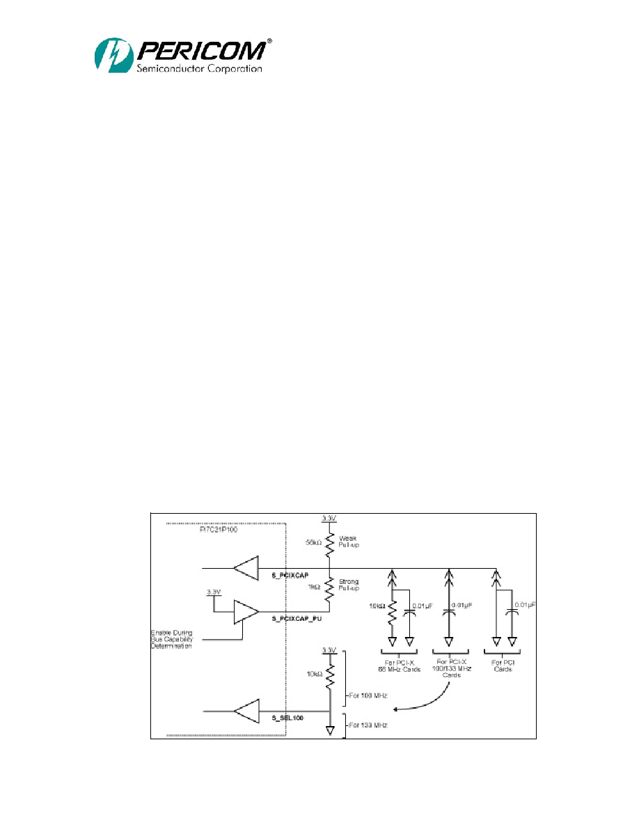
PI7C21P100
2-PORT PCI-X BRIDGE
ADVANCE INFORMATION
Page 35 of 77
June 10, 2005 Revision 1.06
6.3.2
SECONDARY BUS
The secondary interface is capable of operating in either conventional PCI mode or in PCI-X
mode. PI7C21P100 controls the mode and frequency for the secondary bus by utilizing a pull-
up circuit connected to S_PCIXCAP. There are two pull-up resistors in the circuit as
recommended by the PCI-X addendum. The first resistor is a weak pull-up (56K ohms)
whose value is selected to set the voltage of S_PCIXCAP below its low threshold when a
PCI-X 66 device is attached to the secondary bus. The second resistor is a strong pull-up,
externally wired between S_PCIXCAP and S_PCIXCAP_PU. The value of the resistor (1K
ohm) is selected to set the voltage of S_PCIXCAP above its high threshold when all devices
on the secondary are PCI-X 66 capable. To detect the mode and frequency of the secondary
bus, S_PCIXCAP_PU is initially disabled and PI7C21P100 samples the value on
S_PCIXCAP.
If PI7C21P100 sees a logic LOW on S_PCIXCAP, one or more devices on the secondary
have either pulled the signal to ground (PCI-X 66 capable) or tied it to ground (only capable
of conventional PCI mode). To differentiate between the two conditions, PI7C21P100 then
enables S_PCIXCAP_PU to put the strong pull-up into the circuit. If S_PCIXCAP remains at
a logic LOW, it must be tied to ground by one or more devices, and the bus is initialized to
conventional PCI mode. If S_PCIXCAP_PU can be pulled up, one or more devices are
capable of only PCI-X 66 operation so the bus is initialized to PCI-X 66 mode. If
PI7C21P100 sees a logic HIGH on S_PCIXCAP, then all devices on the secondary bus are
capable of PCI-X 133 operation. PI7C21P100 then samples S_SEL100 to distinguish between
the 66-100 MHz and the 100-133 MHz clock frequency ranges. If PI7C21P100 sees logic
HIGH on S_SEL100, the secondary bus is initialized to PCI-X 100 mode. If the value is
LOW, PCI-X 133 is initialized. These two ranges allow adjustment of the clock frequency to
account for bus loading conditions.
There is no pin for M66EN for the secondary interface on PI7C21P100 because the internal
PLL is bypassed in conventional PCI mode. S_CLK is used directly, eliminating the need to
distinguish between conventional PCI 33 and conventional PCI 66.
Table 6-1 PROGRAMMABLE PULL-UP CIRCUIT
PI7C21P100
2-PORT PCI-X BRIDGE
ADVANCE INFORMATION
Page 36 of 77
June 10, 2005 Revision 1.06
6.3.3
CLOCK STABILITY
To comply with PCI and PCI-X architecture specifications, the bus clock must be stable and
running at the designated frequency for at least 100us after deassertion of the bus reset.
S_CLK_STABLE is used to determine and detect when S_CLK has become stable. During a
bus reset, PI7C21P100 will wait for the assertion of S_CLK_STABLE before determining the
mode and frequency. PI7C21P100 is expecting no more than one transition on the
S_CLK_STABLE input from the "not stable" to the "stable" state. S_CLK_STABLE input
may be tied HIGH if the secondary clock input is known to be always stable prior to the
deassertion of the primary bus reset signal or the secondary bus reset bit of the bridge control
register. Examples of sources for S_CLK_STABLE are lock indicators on circuits that
employ PLL's or "power good" indicators.
6.3.4
DRIVER IMPEDANCE SELECTION
The output drivers on PI7C21P100 are capable of two different output impedances, 40 ohm
output impedance and a 20 ohm. The output impedance for the primary and secondary
interfaces is separately controlled. PI7C21P100 selects a default impedance value at the
deassertion of the bus reset based on the bus mode and frequency. If a bus is configured to be
in PCI-X 133 mode, it is assumed that the bus will have fewer devices and have a higher
impedance. In this case, the drivers utilize the 40 ohm output impedance mode. The 20 ohm
output impedance mode is utilized for all other PCI-X and all PCI configurations, assuming
that the bus is more heavily loaded and has lower impedance. Some applications do not
follow these assumptions so two control signals are provided; P_DRVR for the primary and
S_DRVR for the secondary. When these inputs are pulled HIGH, PI7C21P100 will change
the output impedance of the drivers on their respective interfaces to the opposite state than
was assumed by default, as shown in Table 6-2. The driver mode may not be changed
dynamically, but can be changed during each bus reset.
Table 6-2 DRIVER IMPEDANCE SELECTION
Primary Bus
Mode
Default Driver
Mode
(P_DRVR=0)
Driver Mode if
(P_DRVR=1)
Secondary Bus
Mode
Default Driver
Mode
(S_DRVR=0)
Driver Mode if
(S_DRVR=1)
Conventional
PCI
20 ohm
40 ohm
Conventional
PCI
20 ohm
40 ohm
PCI-X 66
20 ohm
40 ohm
PCI-X 66
20 ohm
40 ohm
PCI-X 100
20 ohm
40 ohm
PCI-X 100
20 ohm
40 ohm
PCI-X 133
20 ohm
20 ohm
PCI-X 133
40 ohm
20 ohm
7
RESET
The primary and secondary interface each have their own asynchronous reset signal used at
power-on and at other times to put PI7C21P100 into a known state. The reset signal on the
primary (P_RST#) is an input pin, while the reset signal on the secondary (S_RST#) is an
output pin driven by PI7C21P100.

PI7C21P100
2-PORT PCI-X BRIDGE
ADVANCE INFORMATION
Page 37 of 77
June 10, 2005 Revision 1.06
7.1
PRIMARY INTERFACE RESET
When P_RST# is asserted, the following events occur:
PI7C21P100 immediately tri-states all primary PCI interface signals. S_AD[31:0] and
S_CBE[3:0] are driven LOW on the secondary interface and other control signals are tri-
stated.
PI7C21P100 performs a chip reset.
Registers that have default values are reset.
PI7C21P100 is not accessible during P_RST#. After P_RST# is deasserted in PCI-X mode,
PI7C21P100 remains inaccessible for 100us to enable the internal PLL to lock to its target
frequency. In conventional PCI mode, PI7C21P100 is held in reset 7 PCI clocks after the
deassertion of P_RST#.
7.2
SECONDARY INTERFACE RESET
PI7C21P100 is responsible for driving the secondary bus reset signals, S_RST#. PI721P100
asserts S_RST# when any of the following conditions are met:
Signal P_RST# is asserted. Signal S_RST# remains asserted as long as P_RST# is asserted
and does not de-assert until P_RST# is de-asserted.
The secondary reset bit in the bridge control register is set. Signal S_RST# remains
asserted until a configuration write operation clears the secondary reset bit.
Several things must occur at or prior to the de-assertion of S_RST#. Once P_RST# is
de-asserted or the secondary bus reset bit is changed from 1 to 0, PI7C21P100 will wait for
the S_CLK_STABLE signal to be asserted before proceeding. S_CLK must be stable at a
frequency within the bus capability limits prior to the assertion of S_CLK_STABLE. Since
the PCI Local Bus Specification requires that the bus clock be stable for at least 100us prior to
the de-assertion of the bus reset, S_CLK_STABLE serves as a gate to a timer that ensures that
this requirement is met. During this time delay period, the secondary bus mode and frequency
is determined through the programmable pull-up circuit. This process may include up to 80us
for the capacitive load on S_PCIXCAP to be charged. By the time the 100us timer expires,
the bus mode and frequency will have been determined. The S_RST# signal is then
de-asserted a minimum of ten secondary bus PCI clock cycles later.
When the secondary bus is operating in PCI-X mode, an internal PLL is used to source the
clock tree for the secondary clock domain inside PI7C21P100. The appropriate range and
tuning bits for the PLL are set once the mode and frequency are determined, and an internal
PLL reset signal is deactivated to allow the PLL to begin locking to the S_CLK input
frequency. The PLL requires an allowance of 100us to accomplish this frequency lock. An
internal reset is held on the logic in the secondary clock domain until this time period has
elapsed. While the internal reset is active, PI7C21P100 will not respond to any secondary bus
transactions. When the secondary bus is operating in PCI mode, the internal PLL for the
secondary interface is not used. The internal PLL reset remains activated, keeping the PLL in
the bypass mode, and the internal logic reset is held for 5 additional secondary PCI clock
cycles.
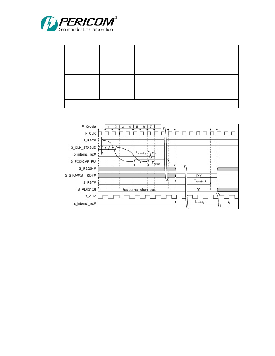
PI7C21P100
2-PORT PCI-X BRIDGE
ADVANCE INFORMATION
Page 38 of 77
June 10, 2005 Revision 1.06
Table 7-1 DELAY TIMES FOR DE-ASSERTION OF S_RST#
Conventional PCI
PCI-X 66
PCI-X 100
PCI-X 133
T
PIRSTDLY
7 primary clock
cycles
6678 primary clock
cycles
100us 133us
13350 primary
clock cycles
133us 200us
13350 primary
clock cycles
100us 133us
T
XCAP
6675 primary clock
cycles
6675 primary clock
cycles
100us 133us
13347 primary
clock cycles
133us 200us
13347 primary
clock cycles
100us 133us
T
SRSTDLY
11 secondary and 7
primary clock
cycles
11 secondary and 7
primary clock
cycles
11 secondary and 7
primary clock
cycles
11 secondary and 7
primary clock
cycles
T
SIRSTDLY
16 secondary clock
cycles
6687 secondary
clock cycles
100us 133us
13350 secondary
clock cycles
133us 200us
13350 secondary
clock cycles
100us 133us
Note: Primary and secondary clock cycles refer to clock cycles whose period is determined by the P_CLK and
S_CLK inputs.
Table 7-2 DE-ASSERTION OF S_RST#
7.3
BUS PARKING & BUS WIDTH DETERMINATION
Bus parking refers to driving the AD[31:0], CBE[3:0], and PAR lines to a known value while
the bus is idle. In general, the device implementing the bus arbiter is responsible for parking
the bus or assigning another device to park the bus. A device parks the bus when the bus is
idle, its bus grant is asserted, and the device's request is not asserted. The AD[31:0],
CBE[3:0], and PAR signals are driven LOW after assertion of S_RST#.
PI7C21P100 will assert S_REQ64# for at least 10 PCI clock cycles to allow devices to
determine whether they are connected on a 64-bit bus or 32-bit bus.
7.4
SECONDARY DEVICE MASKING
Secondary devices can be masked through configuration or power strapping of the secondary
bus private device mask register. The process of converting Type 1 configuration transactions
to Type 0 configuration transactions is modified by the contents of the secondary bus private
device mask register. A configuration transaction that targets a device masked by this register
is routed to device 15. Secondary bus architectures which are designed to support masking of

PI7C21P100
2-PORT PCI-X BRIDGE
ADVANCE INFORMATION
Page 39 of 77
June 10, 2005 Revision 1.06
devices should not implement a device number 15 (i.e., S_AD(31)). The device mask bit
options (device numbers 1, 4, 5, 6, 7, 9, and 13) defined by PI7C21P100 allow architectures
to support private device groupings that use a single or multiple interrupt binding.
7.5
ADDRESS PARITY ERRORS
PI7C21P100 checks address parity for all transactions on both buses, for all address and all
bus commands. When PI7C21P100 detects an address parity error, the transaction will not be
claimed and will be allowed to terminate with a master abort. The result of an address parity
error will be controlled by the parity error response bits in both the command and bridge
control registers.
7.6
OPTIONAL BASE ADDRESS REGISTER
The 64 bit Base Address register located in the configuration register at offsets 10h and 14h
can optionally be used to acquire a 1 MB memory region at system initialization. PI7C21P100
uses this register to claim an additional prefetchable memory region for the secondary bus.
When used with the secondary device masking, this allows for the acquisition of memory
space for private devices that are not otherwise viewable by the system software.
This 64 bit base address register and the memory space defined by it are enabled by the
BAR_EN. When BAR_EN is pulled LOW, this register location returns zeros for reads and
cannot be written. When BAR_EN is pulled HIGH, the upper memory base address register
and lower memory base address registers combined specify address bits 63:20 of a memory
region. Memory accesses on the primary bus are compared against this register, if address bits
63:20 are equal to bits 63:20 of the address defined by the combination of the lower memory
base address register and the upper memory base address register, the access is claimed by
PI7C21P100 and passed through to the secondary bus. Memory accesses on the secondary bus
are also compared against this register, if address bits 63:20 are equal to bits 63:20 of the
address defined by the combination of the lower memory base address register and the upper
memory base address register, the access is ignored by the bridge.
7.7
OPTIONAL CONFIGURATION ACCESS FROM THE
SECONDARY BUS
PI7C21P100 accepts Type 0 configuration transactions when the following conditions are met
during the address phase:
S_CBE[3:0]# indicates a configuration read or configuration write transaction
S_AD[1:0] are 00
S_IDSEL is asserted
Applications that require access to the bridge configuration registers via the secondary bus
may control the initialization sequence through the P_CFG_BUSY pin and bit[2] offset 44h of
the miscellaneous control register. When P_CFG_BUSY is pulled HIGH, bit[2] offset 44h is
set to 1b at power up and reset. This causes PI7C21P100 to retry Type 0 configuration
transactions on the primary bus that would otherwise be accepted. PI7C21P100 continues to
retry these transactions until bit[2] offset 44h is set to 0b by a configuration write initiated on
the secondary bus. This allows a device on the secondary bus to initialize the bridge and any
private devices on the secondary bus without contention from devices accessing the bridge

PI7C21P100
2-PORT PCI-X BRIDGE
ADVANCE INFORMATION
Page 40 of 77
June 10, 2005 Revision 1.06
through the primary bus. Applications that do not require access to the bridge configuration
registers via the secondary bus should pull both the S_IDSEL and P_CFG_BUSY pins LOW.
7.8
SHORT TERM CACHING
Short Term Caching is a means to provide performance improvements where upstream
devices are not able to stream data continuously to meet the prefetching needs of the
PI7C21P100. When the master completes the transaction, the bridge is required to discard the
balance of any data that was prefetched for the master. To prevent performance impacts when
dealing with target devices that can only stream data of 128 to 512 bytes before
disconnecting, PI7C21P100 utilizes Short Term Caching. This feature applies only when the
secondary bus is operating in conventional PCI mode and provides a time limited read data
cache in which the bridge will not discard prefetched read data after the request has been
completed on the initiating bus. Short Term Caching is an optional feature which is enabled
by setting bit[8] and bit[15] offset B8h of the Miscellaneous Control Register 2. When
enabled, PI7C21P100 will not discard the additional prefetched data when the read transaction
has been completed on the initiating bus. PI7C21P100 will continue to prefetch data up to the
amount specified by bits [30:28] offset 40h of the Secondary Data Buffering Control Register.
Should the initiator generate a new transaction requesting the previously prefetched data,
PI7C21P100 will return that data. PI7C21P100 will discard the data approximately 64
secondary clocks after some of the data for a request has been returned to the initiator, and the
initiator has not requested additional data. This feature applies to all secondary devices if
enabled. System designers need to ensure that all attached devices have memory region(s) that
are architected to be accessed by only one master and that the additional prefetching will
present data to the initiator in the same state as if the initial transaction were continued. This
feature should only be used in system designs that are able to ensure that the data provided to
the master has not been modified since the initial transaction.
PI7C21P100
2-PORT PCI-X BRIDGE
ADVANCE INFORMATION
Page 41 of 77
June 10, 2005 Revision 1.06
8
CONFIGURATION REGISTERS
PCI configuration defines a 64 DWORD space to define various attributes of PI7C21P100.
8.1
CONFIGURATION REGISTER SPACE MAP
Table 8-1 CONFIGURATION SPACE MAP
Bit Number
31 24
23 16
15 8
7 - 0
DWORD
Address
Device ID
Vendor ID
00h
Primary Status
Primary Command
04h
Class Code
Revision ID
08h
BIST
Header Type
Primary Latency Timer
Cache Line Size
0Ch
Lower Memory Base Address
10h
Upper Memory Base Address
14h
Secondary Latency
Timer
Subordinate Bus
Number
Secondary Bus Number
Primary Bus Number
18h
Secondary Status
I/O Limit
I/O Base
1Ch
Memory Limit
Memory Base
20h
Prefetchable Memory Limit
Prefetchable Memory Base
24h
Prefetchable Base Upper 32-bit
28h
Prefetchable Limit Upper 32-bit
2Ch
I/O Limit Upper 16-bit
I/O Base Upper 16-bit
30h
Reserved Capability
Pointer
34h
Expansion ROM Base Address
38h
Bridge Control
Interrupt Pin
Interrupt Line
3Ch
Secondary Data Buffering Control
Primary Data Buffering Control
40h
Reserved Miscellaneous
Control
44h
Reserverd
Extended Chip Control
2
Extended Chip Control
1
48h
Reserved
4Ch
Reserved Arbiter
Mode
50h
Reserved Arbiter
Enable
54h
Reserved Arbiter
Priority
58h
Reserved SERR#
Disable
5Ch
Primary Retry Counter
60h
Secondary Retry Counter
64h
Reserved
Discard Timer Control
68h
Reserved
Retry and Timer Status
6Ch
Reserved Opaque
Memory
Enable
70h
Opaque Memory Limit
Opaque Memory Base
74h
Opaque Memory Base Upper 32-bit
78h
Opaque Memory Limit Upper 32-bit
7Ch
PCI-X Secondary Status
Next Capability Pointer
PCI-X Capability ID
80h
PCI-X Bridge Status
84h
Secondary Bus Upstream Split Transaction
88h
Primary Bus Downstream Split Transaction
8Ch
Power Management Capabilities
Next Capabilities
Pointer
Power Management ID
90h
PCI-to-PCI Bridge Support Extension
Power Management Control and Status
94h
Reserved
98h-Ach
Secondary Bus Private Device Mask
B0h
Reserved
B4h
Reserved
Miscellaneous Control 2
B8h
Reserved
BCh-FFh
PI7C21P100
2-PORT PCI-X BRIDGE
ADVANCE INFORMATION
Page 42 of 77
June 10, 2005 Revision 1.06
8.1.1.1
SIGNAL TYPE DEFINITION
SIGNAL TYPE
DEFINITION
RO READ
ONLY
RW
READ / WRITE
RWC
READ / WRITE 1 TO CLEAR
8.1.2
VENDOR ID REGISTER OFFSET 00h
BIT FUNCTION
TYPE
DESCRIPTION
15:0
Vendor ID
RO
Identifies Pericom as the vendor of this device. Hardwired as 12D8h
8.1.3
DEVICE ID REGISTER OFFSET 00h
BIT FUNCTION
TYPE
DESCRIPTION
31:16
Device ID
RO
Identifies the device as PI7C21P100. Hardwired as 01A7h.
8.1.4
COMMAND REGISTER OFFSET 04h
BIT FUNCTION
TYPE
DESCRIPTION
15:10
Reserved
RO
Reserved. Returns 000000 when read.
9 Fast
Back-to-Back
Enable
RO
Fast Back-to-Back Control
0: Prohibits PI7C21P100 to initiate fast back-to-back transactions on
the primary
This bit is ignored in PCI-X mode. Reset to 0
8 P_SERR#
Enable RW
System Error Control
0: Disables the P_SERR# driver on the primary
1: Enables the P_SERR# driver on the primary
Reset to 0
7
Wait Cycle Control
RO
Wait Cycle Control
0: Address/data stepping is disabled (primary and secondary)
This bit is ignored in PCI-X mode. Returns 0 when read.
6
Parity Error Response
RW
Parity Error Response
0: PI7C21P100 may ignore any detected parity errors and continue
normal operation
1: PI7C21P100 must take its normal action when a parity error is
detected.
Reset to 0
5
VGA Palette Snoop
Enable
RW
VGA Palette Snoop Control
0: Ignore VGA palette accesses on the primary
1: Enables positive decoding response to VGA palette writes on the
primary with I/O address bits AD[9:0] equal to 3C6h, 3C8h, and
3C9h (inclusive of ISA aliases; AD[15:10] are not decoded and may
be any value.
Reset to 0
4
Memory Write and
Invalidate Enable
RO
Memory Write and Invalidate Control
0: Disables Memory Write and Invalidate transactions. PI7C21P100
does not generate memory write and invalidate transactions.
This bit is ignored in PCI-X mode. Returns 0 when read.
3 Special
Cycle
Enable
RO
Special Cycle Control
0: PI7C21P100 does not respond as a target to Special Cycle
transactions.
Returns 0 when read.

PI7C21P100
2-PORT PCI-X BRIDGE
ADVANCE INFORMATION
Page 43 of 77
June 10, 2005 Revision 1.06
BIT FUNCTION
TYPE
DESCRIPTION
2 Bus
Master
Enable RW
Bus Master Control
0: PI7C21P100 does not initiate memory and I/O transactions on the
primary and disables responses to memory and I/O transactions on
the secondary
1: Enables PI7C21P100 to operate as a master on the primary for
memory and I/O transactions forwarded from the secondary.
In PCI-X mode, PI7C21P100 is allowed to initiate a split completion
transaction regardless of the status of this bit. Reset to 0
1
Memory Space Enable
RW
Memory Space Control
0: Ignore memory transactions on the primary
1: Enables responses to memory transactions on the primary
Reset to 0
0
I/O Space Enable
RW
I/O Space Control
0: Ignores I/O transactions on the primary
1: Enables responses to I/O transaction on the primary
Reset to 0
8.1.5
PRIMARY STATUS REGISTER OFFSET 04h
BIT FUNCTION
TYPE
DESCRIPTION
31
Detected Parity Error
RWC
Detected Parity Error Status
0: Address or data parity error not detected by PI7C21P100
1: Address or data parity error detected by PI7C21P100
Reset to 0
30
Signaled System Error
RWC
Signaled System Error Status
0: PI7C21P100 did not assert SERR#
1: PI7C21P100 asserted SERR#
Reset to 0
29 Received
Master
Abort
RWC
Received Master Abort Status
0: Transaction not terminated with a bus master abort
1: Transaction terminated with a bus master abort
Reset to 0
28
Received Target Abort
RWC
Received Target Abort Status
0: Transaction not terminated with a target abort
1: Transaction terminated with a target abort
Reset to 0
27
Signaled Target Abort
RWC
Signaled Target Abort Status
0: Target device did not terminate transaction with a target abort
1: Target device terminated transaction with a target abort
26:25 DEVSEL#
Timing
RO DEVESEL# Timing Status
01: Medium decoding.
Returns 01h when read.
24
Data Parity Error
RWC
Data Parity Error Status
0: No data parity error detected
1: Data parity error detected
Reset to 0
23 Fast
Back-to-Back
Capable
RO
Fast Back-to-Back Status
0: Target not capable of decoding fast back-to-back transactions in
PCI-X mode
1: Target capable of decoding fast back-to-back transactions in
conventional PCI mode
Returns 0 in PCI-X mode and 1 in conventional PCI mode
22 Reserved
RO Reserved. Returns 0 when read.
21 66MHz
Capable
RO 66MHz Capable Status
1: Capable of 66MHz operation
Returns 1 when read.
20
Capability List
RO
Capability List
1: PI7C21P100 supports the capability list and offset 34h is the
pointer to the data structure.
Returns 0 when read.
19:16 Reserved
RO Reserved. Returns 0000 when read.
PI7C21P100
2-PORT PCI-X BRIDGE
ADVANCE INFORMATION
Page 44 of 77
June 10, 2005 Revision 1.06
8.1.6
REVISION ID REGISTER OFFSET 08h
BIT FUNCTION
TYPE
DESCRIPTION
7:0
Revision ID
RO
Specifies the revision of PI7C21P100. Read as 0h
8.1.7
CLASS CODE REGISTER OFFSET 08h
BIT FUNCTION
TYPE
DESCRIPTION
31:24
Class Code
RO
Specifies the base class code for PI7C21P100 identifying it as a
Bridge device according to PCI specifications. Read as 06h
23:16
Sub Class Code
RO
Specifies the sub-class code identifying PI7C21P100 as a Bridge
device. Read as 04h.
15:8 Programming
Interface
RO Subtractive
decoding not supported. Read as 0h
8.1.8
CACHE LINE SIZE REGISTER OFFSET 0Ch
BIT FUNCTION
TYPE
DESCRIPTION
7:0
Cache Line Size
RW
Designates the cache line size for the system and is used when
terminating memory write and invalidate transactions and when
prefetching memory read transactions. Not used in PCI-X mode.
bit[7:6]: Not supported and should be 00b
bit[5]: If 1, then cache line size = 32 DWORDS
bit[4]: If 1, then cache line size = 16 DWORDS
bit[3]: If 1, then cache line size = 8 DWORDS
bit[2]: If 1, then cache line size = 4 DWORDS
bit[1:0]: Not supported and should be 00b
8.1.9
PRIMARY LATENCY TIMER OFFSET 0Ch
BIT FUNCTION
TYPE
DESCRIPTION
15:11
Primary Latency Timer
RW
Designates the upper 5 bits of the primary latency timer in PCI clock
units
10:8
Primary Latency Timer
RO
Designates the lower 3 bits of the primary latency timer in PCI clock
units. Returns 000 when read to force 8-cycle increments for the
latency timer.
8.1.10
HEADER TYPE REGISTER OFFSET 0Ch
BIT FUNCTION
TYPE
DESCRIPTION
23
Single Function Device
RO
Returns 0 when read to designate single function device
22:16 PCI-to-PCI
Configuration
RO
Returns 0000001 when read.
8.1.11
BIST REGISTER OFFSET 0Ch
BIT FUNCTION
TYPE
DESCRIPTION
31:24
BIST
RO
BIST not supported. Returns 0 when read.

PI7C21P100
2-PORT PCI-X BRIDGE
ADVANCE INFORMATION
Page 45 of 77
June 10, 2005 Revision 1.06
8.1.12
LOWER MEMORY BASE ADDRESS REGISTER OFFSET 10h
BIT FUNCTION
TYPE
DESCRIPTION
31:20
Memory Base Address
RW
Address bits[31:20] of the memory base address if BAR_EN is 1. If
BAR_EN is 0, then this register is reserved and returns zeros when
read.
19:4
Reserved
RO
Reserved. Returns 00h when read
3
Prefetchable Indicator
RO
Identifies the address range defined by this register is prefetchable.
Returns 1 when read
2:1
Decoder Width
RO
Indicates that this is the lower portion of a 64-bit register. Returns
10b when read.
0
Decoder Type
RO
Indicates that this register is a memory decoder. Returns 0 when
read.
8.1.13
UPPER MEMORY BASE ADDRESS REGISTER OFFSET 14h
BIT FUNCTION
TYPE
DESCRIPTION
31:0
Upper Memory Base
Address
RW
Address bits[63:32] of the memory base address if BAR_EN is 1. If
BAR_EN is 0, this register is reserved and returns zeros when read.
8.1.14
PRIMARY BUS NUMBER REGISTER OFFSET 18h
BIT FUNCTION
TYPE
DESCRIPTION
7:0
Primary Bus Number
RW
Records the bus number of the PCI segment that PI7C21P100 is
connected to on the primary side.
Reset to 00h
8.1.15
SECONDARY BUS NUMBER REGISTER OFFSET 18h
BIT FUNCTION
TYPE
DESCRIPTION
15:8
Secondary Bus Number
RW
Records the bus number of the PCI segment that PI7C21P100 is
connected to on the secondary side.
Reset to 00h
8.1.16
SUBORDINATE BUS NUMBER REGISTER OFFSET 18h
BIT FUNCTION
TYPE
DESCRIPTION
23:16 Subordinate
Bus
Number
RW
Records the highest bus number of the PCI segment that resides
behind PI7C21P100.
Reset to 00h
8.1.17
SECONDARY LATENCY TIMER REGISTER OFFSET 18h
BIT FUNCTION
TYPE
DESCRIPTION
31:24 Secondary
Latency
Timer
RW
Specifies the value of the secondary latency timer in PCI bus clock
units.
Reset to 00h in conventional PCI mode
Reset to 40h in PCI-X mode

PI7C21P100
2-PORT PCI-X BRIDGE
ADVANCE INFORMATION
Page 46 of 77
June 10, 2005 Revision 1.06
8.1.18
I/O BASE ADDRESS REGISTER OFFSET 1Ch
BIT FUNCTION
TYPE
DESCRIPTION
7:4
I/O Base Address
RW
Specifies the base of the I/O address range bits [15:12] and is used
with the I/O limit register and I/O base upper 16 bits and I/O limit
upper 16-bit registers
3:2
Reserved
RO
Reserved. Returns 00b when read.
1:0
32-bit I/O Addressing
RO
Returns 01b when read to indicate PI7C21P100 supports 32-bit I/O
addressing
8.1.19
I/O LIMIT REGISTER OFFSET 1Ch
BIT FUNCTION
TYPE
DESCRIPTION
15:12
I/O Limit Address
RW
Address bits[15:12] of the limit address for the address range of I/O
operations that are passed from primary to secondary
11:10
Reserved
RO
Reserved. Returns 00b when read.
9:8
32-bit I/O Addressing
RO
Returns 01b when read to indicate PI7C21P100 supports 32-bit I/O
addressing
8.1.20
SECONDARY STATUS REGISTER OFFSET 1Ch
BIT FUNCTION
TYPE
DESCRIPTION
31
Detected Parity Error
RWC
Detected Parity Error Status
0: Address or data parity error not detected by PI7C21P100 on the
secondary
1: Address or data parity error detected by PI7C21P100 on the
secondary
Reset to 0
30
Signaled System Error
RWC
Signaled System Error Status
0: PI7C21P100 did not assert SERR# on the secondary
1: PI7C21P100 asserted SERR# on the secondary
Reset to 0
29 Received
Master
Abort
RWC
Received Master Abort Status
0: Transaction not terminated with a bus master abort on the
secondary
1: Transaction terminated with a bus master abort on the secondary
Reset to 0
28
Received Target Abort
RWC
Received Target Abort Status
0: Transaction not terminated with a target abort
1: Transaction terminated with a target abort
Reset to 0
27
Signaled Target Abort
RWC
Signaled Target Abort Status
0: Target device did not terminate transaction with a target abort
1: Target device terminated transaction with a target abort
Reset to 0
26:25 DEVSEL#
Timing
RO DEVESEL# Timing Status
01: Medium decoding.
Returns 01h when read.
24
Data Parity Error
RWC
Data Parity Error Status
0: No data parity error detected on the secondary
1: Data parity error detected on the secondary
Reset to 0
23 Fast
Back-to-Back
Enable
RO
Fast Back-to-Back Status
0: Target not capable of decoding fast back-to-back transactions in
PCI-X mode
1: Target capable of decoding fast back-to-back transactions in
conventional PCI mode
Returns 0 in PCI-X mode and 1 in conventional PCI mode
22 Reserved
RO Reserved. Returns 0 when read.
PI7C21P100
2-PORT PCI-X BRIDGE
ADVANCE INFORMATION
Page 47 of 77
June 10, 2005 Revision 1.06
BIT FUNCTION
TYPE
DESCRIPTION
21 66MHz
Capable
RO 66MHz Capable Status
1: Capable of 66MHz operation
Returns 1 when read.
20:16 Reserved
RO Reserved. Returns 00000 when read.
8.1.21
MEMORY BASE REGISTER OFFSET 20h
BIT FUNCTION
TYPE
DESCRIPTION
15:4
Memory Base
RW
Specifies the base of the memory mapped I/O address range
bit[31:20] and is used with the Memory Limit register to specify a
range of 32-bit addresses supported for memory mapped I/O
transactions.
Reset to 800h
3:0 Reserved
RO Reserved. Returns 0 when read
8.1.22
MEMORY LIMIT REGISTER OFFSET 20h
BIT FUNCTION
TYPE
DESCRIPTION
31:20
Memory Limit
RW
Specifies address bits[31:20] of the limit address for the address
range of memory mapped I/O operations.
Reset to 000h
19:16 Reserved
RO Reserved. Returns 0 when read
8.1.23
PREFETCHABLE MEMORY BASE REGISTER OFFSET 24h
BIT FUNCTION
TYPE
DESCRIPTION
15:4 Prefetchable
Memory
Base
RW
Specifies address bits[31:20] of the base address for the address
range of prefetchable memory operations.
Reset to 800h
3:0
64-bit Addressing
RO
Designates 64-bit addressing support. Returns 1h when read.
8.1.24
PREFETCHABLE MEMORY LIMIT REGISTER OFFSET 24h
BIT FUNCTION
TYPE
DESCRIPTION
31:20 Prefetchable
Memory
Limit
RW
Specifies address bits[31:20] of the limit address for the address
range of prefetchable memory operations.
Reset to 800h
19:16
64-bit Addressing
RO
Designates 64-bit addressing support. Returns 1h when read.
8.1.25
PREFETCHABLE BASE UPPER 32-BIT REGISTER OFFSET 28h
BIT FUNCTION
TYPE
DESCRIPTION
31:0 Prefetchable
Base
Upper 32-bit
RW
Specifies address bits[63:32] of the base address for the address
range of prefetchable memory operations.
Reset to 0000 0000h
PI7C21P100
2-PORT PCI-X BRIDGE
ADVANCE INFORMATION
Page 48 of 77
June 10, 2005 Revision 1.06
8.1.26
PREFETCHABLE LIMIT UPPER 32-BIT REGISTER OFFSET 2Ch
BIT FUNCTION
TYPE
DESCRIPTION
31:0 Prefetchable
Limit
Upper 32-bit
RW
Specifies address bits[63:32] of the limit address for the address
range of prefetchable memory operations.
Reset to 0000 0000h
8.1.27
I/O BASE UPPER 16-BIT REGISTER OFFSET 30h
BIT FUNCTION
TYPE
DESCRIPTION
15:0
I/O Base Upper 16-bit
RW
Specifies address bits[31:16] of the base address for the address
range of I/O operations.
Reset to 0000h
8.1.28
I/O LIMIT UPPER 16-BIT REGISTER OFFSET 30h
BIT FUNCTION
TYPE
DESCRIPTION
31:16
I/O Limit Upper 16-bit
RW
Specifies address bits[31:16] of the limit address for the address
range of I/O operations.
Reset to 0000h
8.1.29
CAPABILITY POINTER OFFSET 34h
BIT FUNCTION
TYPE
DESCRIPTION
7:0 Capability
Pointer RO Pointer to a capabilities list in the configuration space. Returns 80h
when read.
8.1.30
EXPANSION ROM BASE ADDRESS REGISTER OFFSET 38h
BIT FUNCTION
TYPE
DESCRIPTION
31:0
Expansion ROM Base
Address
RO
Expansion ROM not supported. Returns 00000000h when read
8.1.31
INTERRUPT LINE REGISTER OFFSET 3Ch
BIT FUNCTION
TYPE
DESCRIPTION
7:0
Interrupt Line Register
RW
For POST program to initialize to FFh, defining PI7C21P100 does
not implement an interrupt pin.
8.1.32
INTERRUPT PIN REGISTER OFFSET 3Ch
BIT FUNCTION
TYPE
DESCRIPTION
15:8
Interrupt Pin Register
RO
Defines the interrupt pin, but PI7C21P100 does not implement any
interrupt pins. Read as 00h.

PI7C21P100
2-PORT PCI-X BRIDGE
ADVANCE INFORMATION
Page 49 of 77
June 10, 2005 Revision 1.06
8.1.33
BRIDGE CONTROL REGISTER OFFSET 3Ch
BIT FUNCTION
TYPE
DESCRIPTION
31:28 RESERVED
RO Reserved. Returns 0h when read.
27 Discard
Timer
P_SERR# Enable
RW
Discard Timer P_SERR# Enable
0: Does not assert P_SERR# on the primary interface as a result of
the expiration of either the primary discard timer or secondary
discard timer.
1: Asserts P_SERR# on the primary interface as a result of the
expiration of either the primary discard timer or secondary discard
timer.
This bit is ignored in PCI-X mode. Reset to 0h.
26
Master Timeout Status
RWC
Master Timeout Status
0: No discard timer error
1: Discard timer error (from primary or secondary discard timer)
This bit remains 0 when in PCI-X mode. Reset to 0h.
25 Secondary
Master
Timeout Status
RW
Secondary Master Timeout Status
0: The secondary discard timer counts 2
15
PCI clock cycles.
1: The secondary discard timer counts 2
10
PCI clock cycles.
If the secondary interface is in PCI-X mode, this bit is ignored.
Reset to 0h.
24 Primary
Master
Timeout
Status
RW
Primary Master Timeout Status
0: The primary discard timer counts 2
15
PCI clock cycles.
1: The primary discard timer counts 2
10
PCI clock cycles.
If the primary interface is in PCI-X mode, this bit is ignored. Reset
to 0h.
23 Fast
Back-to-Back RO Fast Back-to-Back Transaction Enable
Designates PI7C21P100 does not generate fast back-to-back
transactions. Returns 0 when read.
22 Secondary
Interface
Reset
RW
Secondary Interface Reset
0: Does not force the assertion of S_RST# on the secondary interface
1: Forces the assertion of S_RST# on the secondary interface.
Reset to 0h.
21 Master
Abort
Mode RW
Master Abort Mode
0: Do not report master aborts. Returns FFFFFFFFh on reads and
discard data on writes.
1: Report master aborts by signaling target abort if possible or by
asserting SERR# (if enabled).
If in PCI-X mode, PI7C21P100 will return a split completion
message, leaving the host bridge to return FFFFFFFFh on any non-
posted transaction when the non-posted transaction ends in a master
abort.
Reset to 0h.
20 RESERVED
RO Reserved. Returns 0 when read.
19 VGA
Enable
RW
VGA Enable
0: Does not forward VGA compatible memory and I/O addresses
from the primary to secondary interface unless they are enabled for
forwarding by the defined I/O and memory address ranges.
1: Forwards VGA compatible memory and I/O addresses from the
primary to secondary interface (if the I/O enable and Memory enable
bits are set) independent of the defined I/O and memory address
ranges and independent of the ISA enable bit.
18 ISA
Enable
RW
ISA Enable
0: Forward downstream all I/O addresses in the address defined by
the I/O base and limit registers.
1: Forward upstream all I/O addresses in the address range defined
by the I/O base and limit registers that are in the first 64KB of PCI
I/O address space
Reset to 0h.
17 S_SERR#
Enable RW
S_SERR# Enable
0: Disable the forwarding of S_SERR# to P_SERR#
1: Enable the forwarding of S_SERR# to P_SERR#.
Reset to 0h.

PI7C21P100
2-PORT PCI-X BRIDGE
ADVANCE INFORMATION
Page 50 of 77
June 10, 2005 Revision 1.06
BIT FUNCTION
TYPE
DESCRIPTION
16
Parity Error Response
Enable
RW
Parity Error Response Enable
0: Ignore address and data parity errors on the secondary interface.
1: Enable parity error detection on the secondary interface.
8.1.34
PRIMARY DATA BUFFERING CONTROL REGISTER OFFSET 40h
BIT FUNCTION
TYPE
DESCRIPTION
15 RESERVED
RO Reserved. Returns 0h when read.
14:12 Maximum
Memory
Read Byte Count
RW
Maximum Memory Read Byte Count
000: 512 bytes (default)
001: 128 bytes
010: 256 bytes
011: 512 bytes
100: 1024 bytes
101: 2048 bytes
110: 4096 bytes
111: 512 bytes
Maximum byte count is used by PI7C21P100 when generating read
requests on the secondary interface in response to a memory read
operation initiated on the primary interface which is in PCI mode and
bits[9:8], bits[7:6], or bits[5:4] are set to full prefetch.
Reset to 000
11 Enable
Relaxed
Ordering
RW
Relaxed Ordering Enable
0: Relaxed ordering is disabled in conventional PCI mode.
1: At the primary interface, read completions that occur after the first
read completion are allowed to bypass posted writes and complete
with a higher priority in conventional PCI mode.
In PCI-X mode, the relaxed ordering bit in the attribute field will
take precedence. Reset to 0
10 Primary
Special
Delayed Read Mode
Enable
RW
Primary Special Delayed Read Mode Enable
0: Retry any primary master which repeats its transaction with
command code changes.
1: Allows any primary master to change memory command code
(MR, MRL, MRM) after it has received a retry. PI7C21P100 will
complete the memory read transaction and return data back to the
primary bus master if the address and byte enables are the same.
This bit is ignored in PCI-X mode. Reset to 0
9:8
Primary Read Prefetch
Mode
RW
Primary Read Prefetch Mode
00: One cache line prefetch if memory read address is in the
prefetchable range at the primary interface
01: Reserved
10: Full prefetch if memory read address is in the prefetchable range
at the primary interface.
11: Disconnect on the first DWORD.
These bits are ignored in PCI-X mode. Reset to 00
7:6 Primary
Read
Line
Prefetch Mode
RW
Primary Read Line Prefetch Mode
00: One cache line prefetch if memory read line address is in
prefetchable range at the primary interace
01: Reserved
10: Full prefetch if memory read multiple address is in prefetchable
range at the primary interface
11: Reserved.
These bits are ignored if the primary interface is in PCI-X mode.
5:4 Primary
Read
Multiple
Prefetch Mode
RW
Primary Read Multiple Prefetch Mode
00: One cache line prefetch if memory read multiple address is in
prefetchable range at the primary interface.
01: Reserved.
10: Full prefetch if memory read multiple address is in prefetchable
range at the primary interface.
11: Reserved.
These bits are ignored if the primary interface is in PCI-X mode.
Reset to 10.
3:0 RESERVED
RO Reserved. Returns 0000 when read.

PI7C21P100
2-PORT PCI-X BRIDGE
ADVANCE INFORMATION
Page 51 of 77
June 10, 2005 Revision 1.06
8.1.35
SECONDARY DATA BUFFERING CONTROL REGISTER OFFSET
40h
BIT FUNCTION
TYPE
DESCRIPTION
31 RESERVED
RO Reserved. Returns 0h when read.
30.28 Maximum
Memory
Read Byte Count
RW
Maximum Memory Read Byte Count
000: 512 bytes (default)
001: 128 bytes
010: 256 bytes
011: 512 bytes
100: 1024 bytes
101: 2048 bytes
110: 4096 bytes
111: 512 bytes
Maximum byte count is used by PI7C21P100 when generating read
requests on the primary interface in response to a memory read
operation initiated on the secondary interface which is in
conventional PCI mode and bits[9:8], bits[7:6], or bits[5:4] are set to
full prefetch.
Reset to 000
27 Enable
Relaxed
Ordering
RW
Relaxed Ordering Enable
0: Relaxed ordering is disabled in conventional PCI mode.
1: At the secondary interface, read completions that occur after the
first read completion are allowed to bypass posted writes and
complete with a higher priority in conventional PCI mode.
In PCI-X mode, the relaxed ordering bit in the attribute field will
take precedence. Reset to 0
26 Secondary
Special
Delayed Read Mode
Enable
RW
Secondary Special Delayed Read Mode Enable
0: Retry any secondary master which repeats its transaction with
command code changes.
1: Allows any secondary master to change memory command code
(MR, MRL, MRM) after it has received a retry. PI7C21P100 will
complete the memory read transaction and return data back to the
primary bus master if the address and byte enables are the same.
This bit is ignored in PCI-X mode. Reset to 0
25:24 Secondary
Read
Prefetch Mode
RW
Secondary Read Prefetch Mode
00: One cache line prefetch if memory read address is in the
prefetchable range at the secondary interface
01: Reserved
10: Full prefetch if memory read address is in the prefetchable range
at the secondary interface.
11: Disconnect on the first DWORD.
These bits are ignored in PCI-X mode. Reset to 00
23:22 Secondary
Read
Line
Prefetch Mode
RW
Secondary Read Line Prefetch Mode
00: One cache line prefetch if memory read line address is in
prefetchable range at the secondary interface
01: Reserved
10: Full prefetch if memory read multiple address is in prefetchable
range at the secondary interface
11: Reserved.
These bits are ignored if the secondary interface is in PCI-X mode.
21:20 Secondary
Read
Multiple Prefetch Mode
RW
Secondary Read Multiple Prefetch Mode
00: One cache line prefetch if memory read multiple address is in
prefetchable range at the secondary interface.
01: Reserved.
10: Full prefetch if memory read multiple address is in prefetchable
range at the secondary interface.
11: Reserved.
These bits are ignored if the secondary interface is in PCI-X mode.
Reset to 10.
19:16 RESERVED
RO Reserved. Returns 0000 when read.

PI7C21P100
2-PORT PCI-X BRIDGE
ADVANCE INFORMATION
Page 52 of 77
June 10, 2005 Revision 1.06
8.1.36
MISCELLANEOUS CONTROL REGISTER OFFSET 44h
BIT FUNCTION
TYPE
DESCRIPTION
7:3 RESERVED
RO Reserved. Returns 00000 when read.
2 Primary
Configuration
Busy
RW
Primary Configuration Busy
0: Type 0 configuration commands accepted normally on the primary
interface.
1: Type 0 configuration commands retried on the primary interface.
This bit can be read from both the primary and secondary buses, but
written only from the secondary bus.
Reset value is based on P_CFG_BUSY. If P_CFG_BUSY is tied
HIGH, reset to 1.
1
Data Parity Error
Recovery Enable
RW
Data Parity Error Recovery Enable
0: All PI7C21P100 to pass parity errors through.
1: Cause SERR# to be asserted whenever either master-data-parity-
error bit[8] is set.
Reset to 1.
0
Parity Error Behavior
RW
Parity Error Behavior
0: PI7C21P100 will pass the corrupted data sequence and PERR#
will be asserted (if enabled), but PI7C21P100 will not complete the
data and CBE# for performing completion on the initiating bus when
detecting a data parity error on a non-posted write transaction.
1: Transaction will be completed on the originating bus, PERR# will
be asserted (if enabled), he appropriate status bits will be set, the data
will be discarded and no request will be queued.
Reset to 1.
8.1.37
EXTENDED CHIP CONTROL REGISTER 1 OFFSET 48h
BIT FUNCTION
TYPE
DESCRIPTION
7 RESERVED
RO
Reserved. Returns 0 when read.
6 Bridge
Disconnect
Discard Timer
RW
Bridge Disconnect Discard Control
0: PI7C21P100 will discard remaining data after it disconnects the
external master during burst memory reads transaction on the PCI
source bus.
1: PI7C21P100 will keep remaining data after it disconnects the
external master during burst memory reads on the PCI source bus,
until the external master returns or the discard timer expires.
Reset to 0.
5 Memory
Write
Transaction Entry
Control
RW
Memory Write Transaction Entry Control
0: PI7C21P100 can accept 4 memory write transactions
1: PI7C21P100 can accept 8 memory write transactions
Reset to 0.
4 Synchronous
Mode
Enable
RW
Synchronous Mode Enable
0: Synchronous mode is disabled, and the asynchronous clock input
is supported.
1: Synchronous mode is enabled and is used to decrease the
frequency to frequency latency when PI7C21P100 is forwarding
transactions through the bridge. The clock inputs have to be
synchronized and the primary clock need to lead the secondary clock
with the following combinations:
Primary Secondary time
33MHz 33MHz 0 14ns
66MHz 66MHz 0 7ns
66MHz 33MHz 3 14ns
133MHz 133MHz 0 3ns
133MHz 66MHz 3 7ns
Reset to 0
3 Upstream
Memory
Read
Prefetching Dynamic
Control
RW
Upstream Memory Read Prefetching Dynamic Control
0: Enable upstream memory read prefetching dynamic control
1: Disable upstream memory read prefetching dynamic control
Reset to 0
(Described in section 4.3.6)

PI7C21P100
2-PORT PCI-X BRIDGE
ADVANCE INFORMATION
Page 53 of 77
June 10, 2005 Revision 1.06
BIT FUNCTION
TYPE
DESCRIPTION
2 Downstream
Memory
Read Prefetching
Dynamic Control
RW
Downstream Memory Read Prefetching Dynamic Control
0: Enable downstream memory read prefetching dynamic control
1: Disable downstream memory read prefetching dynamic control
Reset to 0
(Described in section 4.3.6)
1:0 RESERVED
RO Reserved. Returns 00 when read.
8.1.38
EXTENDED CHIP CONTROL REGISTER 2 OFFSET 48h
BIT FUNCTION
TYPE
DESCRIPTION
11:10
Minimum Free Space in
Memory Data FIFO
Control (Secondary)
RW
Minimum Free Space in Memory Data FIFO Control
(Secondary)
Selects the minimum free space in the memory data FIFO to accept
memory writes on the secondary bus in PCI-X mode
00: 128 bytes of free space to accept memory writes
01: 256 bytes of free space to accept memory writes
10: 512 bytes of free space to accept memory writes
11: 128 bytes of free space to accept memory writes
Reset to 00
9:8
Minimum Free Space in
Memory Data FIFO
Control (Primary)
RW
Minimum Free Space in Memory Data FIFO Control (Primary)
Selects the minimum free space in the memory data FIFO to accept
memory writes on the primary bus in PCI-X mode
00: 128 bytes of free space to accept memory writes
01: 256 bytes of free space to accept memory writes
10: 512 bytes of free space to accept memory writes
11: 128 bytes of free space to accept memory writes
Reset to 00
8.1.39
ARBITER MODE REGISTER OFFSET 50h
BIT FUNCTION
TYPE
DESCRIPTION
15:8 Arbiter
Fairness
Counter
RW
Arbiter Fairness Counter
These bits are the initialization value of a counter used by the internal
arbiter. It controls the number of PCI bus cycles that the arbiter holds
a device's PCI bus grant active after detecting a PCI bus request from
another device. The counter is reloaded whenever a new PCI bus
grant is asserted. For every new PCI bus grant, the counter is armed
to decrement when it detects the de-assertion of FRAME#. If the
arbiter fairness counter is set to 00h, the arbiter will not remove a
device's PCI bus grant until the device has de-asserted its PCI bus
request.
Reset to 08h
7
GNT# Output Toggling
Enable
RW
GNT# Output Toggling Enable
0: GNT# not de-asserted after granted master asserts FRAME#
1: GNT# de-asserts for 1 clock after 2 clocks from the granted master
asserting FRAME#.
Reset to 0
6
Broken Master Refresh
RW
Broken Master Refresh
0: A broken master will be ignored forever except when it de-asserts
its REQ# for at least 1 clock
1: Refresh broken master state after all other masters have been
served once.
Reset to 0
5:2 RESERVED
RO Reserved. Returns 0000 when read.
1 Broken
Master
Timeout
Enable
RW
Broken Master Timeout Enable
0: Broken master timeout disabled
1: Broken master timeout enabled. This enables the internal arbiter to
count 16 PCI bus cycles while waiting for FRAME# to become
active when a device's PCI bus GNT# is active and the PCI bus is
idle. If the broken master timeout expires, the PCI bus GNT# for the
device is de-asserted.
Reset to 0

PI7C21P100
2-PORT PCI-X BRIDGE
ADVANCE INFORMATION
Page 54 of 77
June 10, 2005 Revision 1.06
BIT FUNCTION
TYPE
DESCRIPTION
0 External
Arbiter RO
External Arbiter
0: Enable internal arbiter.
1: Disable internal arbiter.
Reset to 0 or 1 according to the value of S_ARB# during the reset. If
S_ARB# is tied LOW, then returns 0 when read. If S_ARB# is tied
HIGH, then returns 1 when read.
8.1.40
ARBITER ENABLE REGISTER OFFSET 54h
BIT FUNCTION
TYPE
DESCRIPTION
7 RESERVED
RO
Reserved. Returns 0 when read.
6
Enable Arbiter 6
RW
Enable Arbiter 6
0: Disable arbitration for master 6
1: Enable arbitration for master 6
Reset to 1
5
Enable Arbiter 5
RW
Enable Arbiter 5
0: Disable arbitration for master 5
1: Enable arbitration for master 5
Reset to 1
4
Enable Arbiter 4
RW
Enable Arbiter 4
0: Disable arbitration for master 4
1: Enable arbitration for master 4
Reset to 1
3
Enable Arbiter 3
RW
Enable Arbiter 3
0: Disable arbitration for master 3
1: Enable arbitration for master 3
Reset to 1
2
Enable Arbiter 2
RW
Enable Arbiter 2
0: Disable arbitration for master 2
1: Enable arbitration for master 2
Reset to 1
1
Enable Arbiter 1
RW
Enable Arbiter 1
0: Disable arbitration for master 1
1: Enable arbitration for master 1
Reset to 1
0
Enable Arbiter 0
RW
Enable Arbiter 0
0: Disable arbitration for internal bridge request
1: Enable arbitration for internal bridge request
Reset to 1
8.1.41
ARBITER PRIORITY REGISTER OFFSET 58h
BIT FUNCTION
TYPE
DESCRIPTION
7 RESERVED
RO
Reserved. Returns 0 when read.
6
Arbiter Priority 6
RW
Arbiter Priority 6
0: Low priority request to master 6
1: High priority request to master 6
Reset to 0
5
Arbiter Priority 5
RW
Arbiter Priority 5
0: Low priority request to master 5
1: High priority request to master 5
Reset to 0
4
Arbiter Priority 4
RW
Arbiter Priority 4
0: Low priority request to master 4
1: High priority request to master 4
Reset to 0
3
Arbiter Priority 3
RW
Arbiter Priority 3
0: Low priority request to master 3
1: High priority request to master 3
Reset to 0

PI7C21P100
2-PORT PCI-X BRIDGE
ADVANCE INFORMATION
Page 55 of 77
June 10, 2005 Revision 1.06
BIT FUNCTION
TYPE
DESCRIPTION
2
Arbiter Priority 2
RW
Arbiter Priority 2
0: Low priority request to master 2
1: High priority request to master 2
Reset to 0
1
Arbiter Priority 1
RW
Arbiter Priority 1
0: Low priority request to master 1
1: High priority request to master 1
Reset to 0
0
Arbiter Priority 0
RW
Arbiter Priority 0
0: Low priority request to internal bridge
1: High priority request to internal bridge
Reset to 1
8.1.42
SERR# DISABLE REGISTER OFFSET 5Ch
BIT FUNCTION
TYPE
DESCRIPTION
7:5 RESERVED
RO Reserved. Returns 000 when read.
4
PERR# on Posted
Writes SERR# Disable
RW
PERR# on Posted Writes SERR# Disable
0: Assert SERR# and set bit[30] offset 04h of the status register if
bit[8] offset 04h in the command register is set. Discard the delayed
transaction.
1: Disable the assertion of SERR#.
Reset to 0
3
Primary Discard Timer
SERR# Disable
RW
Primary Discard Timer SERR# Disable
0: Assert SERR# and update bit[30] offset 04h of the status register
if the primary discard timer expires and bit[8] offset 04h in the
command register is set and bit[27] offset 3Ch in the control register
is set. Discard the delayed transaction and set bit[3] offset 6Ch of the
retry and timer status register.
1: Disable the assertion of SERR# if the primary discard timer
expires. Discard the delayed transaction and set bit[3] offset 6Ch of
the retry and timer status register.
Reset to 0
2 Secondary
Discard
Timer SERR# Disable
RW
Secondary Discard Timer SERR# Disable
0: Assert SERR# and update bit[30] offset 04h of the status register
if the secondary discard timer expires and bit[8] offset 04h in the
command register is set and bit[27] offset 3Ch in the control register
is set. Discard the delayed transaction and set bit[3] offset 6Ch of the
retry and timer status register.
1: Disable the assertion of SERR# if the primary discard timer
expires. Discard the delayed transaction and set bit[3] offset 6Ch of
the retry and timer status register.
Reset to 0
1
Primary Retry Count
SERR# Disable
RW
Primary Retry Count SERR# Disable
0: Assert SERR# and update bit[30] offset 04h of the status register
if the primary retry counter expires and bit[8] offset 04h in the
command register is set. Discard the transaction and set bit[1] offset
6Ch of the retry and timer status register.
1: Disable the assertion of SERR# if the primary retry counter
expires. Discard the transaction and set bit[1] offset 6Ch of the retry
and timer status register.
Reset to 0
0
Secondary Retry Count
SERR# Disable
RW
Secondary Retry Count SERR# Disable
0: Assert SERR# and update bit[30] offset 04h of the status register
if the secondary retry counter expires and bit[8] offset 04h in the
command register is set. Discard the transaction and set bit[0] offset
6Ch of the retry and timer status register.
1: Disable the assertion of SERR# if the primary retry counter
expires. Discard the transaction and set bit[0] offset 6Ch of the retry
and timer status register.
Reset to 0
PI7C21P100
2-PORT PCI-X BRIDGE
ADVANCE INFORMATION
Page 56 of 77
June 10, 2005 Revision 1.06
8.1.43
PRIMARY RETRY COUNTER REGISTER OFFSET 60h
BIT FUNCTION
TYPE
DESCRIPTION
31
2G Retry Count Control
RW
2G Retry Count Control
1: Designates 2G retries before expiration
Reset to 0
30:25 RESERVED
RO Reserved. Returns 000000 when read.
24
16M Retry Count
Control
RW
16M Retry Count Control
1: Designates 16M retries before expiration.
Reset to 0
23:17 RESERVED
RO Reserved. Returns 0000000 when read.
16
64K Retry Count
Control
RW
64K Retry Count Control
1: Designates 64K retries before expiration.
Reset to 0
15:9 RESERVED
RO Reserved. Returns 0000000 when read.
8
256 Retry Count
Control
RW
256 Retry Count Control
1: Designates 256 retries before expiration.
Reset to 0
7:0 RESERVED
RO Reserved. Returns 00000000 when read.
The below settings are the only allowed values. Other settings are not valid and will result in
smaller retry counts. When the counter expires, the bridge discards the requested transaction
on the primary bus and issues SERR# on the primary bus if enabled.
0000 0000: No expiration limit
8000 0000: Allow 2G retries before expiration
0100 0000: Allow 16M retries before expiration
0001 0000: Allow 64K retries before expiration
0000 0100: Allow 256 retries before expiration
8.1.44
SECONDARY RETRY COUNTER REGISTER OFFSET 64h
BIT FUNCTION
TYPE
DESCRIPTION
31
2G Retry Count Control
RW
2G Retry Count Control
1: Designates 2G retries before expiration
Reset to 0
30:25 RESERVED
RO Reserved. Returns 000000 when read.
24
16M Retry Count
Control
RW
16M Retry Count Control
1: Designates 16M retries before expiration.
Reset to 0
23:17 RESERVED
RO Reserved. Returns 0000000 when read.
16
64K Retry Count
Control
RW
64K Retry Count Control
1: Designates 64K retries before expiration.
Reset to 0
15:9 RESERVED
RO Reserved. Returns 0000000 when read.
8
256 Retry Count
Control
RW
256 Retry Count Control
1: Designates 256 retries before expiration.
Reset to 0
7:0 RESERVED
RO Reserved. Returns 00000000 when read.
The below settings are the only allowed values. Other settings are not valid and will result in
smaller retry counts. When the counter expires, the bridge discards the requested transaction
on the secondary bus and issues SERR# on the primary bus if enabled.
0000 0000: No expiration limit
8000 0000: Allow 2G retries before expiration
0100 0000: Allow 16M retries before expiration
0001 0000: Allow 64K retries before expiration
0000 0100: Allow 256 retries before expiration

PI7C21P100
2-PORT PCI-X BRIDGE
ADVANCE INFORMATION
Page 57 of 77
June 10, 2005 Revision 1.06
8.1.45
DISCARD TIMER CONTROL REGISTER OFFSET 68h
BIT FUNCTION
TYPE
DESCRIPTION
7:4 RESERVED
RO Reserved. Returns 0000 when read.
3
Primary Discard Timer
Short Duration
RW
Primary Discard Timer Short Duration
0: Use bit[24] offset 3Ch of the bridge control register to indicate
how many PCI clocks should be allowed before the primary discard
timer expires.
1: 64 PCI clocks allowed before the discard time expires.
Reset to 0
2 Secondary
Discard
Timer Short Duration
RW
Secondary Discard Timer Short Duration
0: Use bit[25] offset 3Ch of the bridge control register to indicate
how many PCI clocks should be allowed before the secondary
discard timer expires.
1: 64 PCI clocks allowed before the secondary discard timer expires.
Reset to 0
1
Primary Discard Timer
Disable
RW
Primary Discard Timer Disable
0: Enable the primary discard timer in conjunction with bit[27] offset
3Ch of the bridge control register
1: Disable the primary discard timer in conjunction with bit[27]
offset 3Ch of the bridge control register
Reset to 0
0 Secondary
Discard
Timer Disable
RW
Secondary Discard Timer Disable
0: Enable the secondary discard timer in conjunction with bit[27]
offset 3Ch of the bridge control register
1: Disable the secondary discard timer in conjunction with bit[27]
offset 3Ch of the bridge control register
Reset to 0
8.1.46
RETRY AND TIMER STATUS REGISTER OFFSET 6Ch
BIT FUNCTION
TYPE
DESCRIPTION
7:4 RESERVED
RO Reserved. Returns 0000 when read.
3
Primary Discard Timer
Status
RW
Primary Discard Timer Status
0: The primary discard timer has not expired since the last reset.
1: The primary discard timer has expired since the last reset.
Reset to 0
2 Secondary
Discard
Timer Status
RW
Secondary Discard Timer Status
0: The secondary discard timer has not expired since the last reset.
1: The secondary discard timer has expired since the last reset.
Reset to 0
1
Primary Retry Counter
Status
RW
Primary Retry Counter Status
0: The primary retry counter has not expired since the last request.
1: The primary retry counter has expired since the last request.
Reset to 0.
0 Secondary
Retry
Counter Status
RW
Secondary Retry Counter Status
0: The secondary retry counter has not expired since the last request.
1: The secondary retry counter has expired since the last request.
Reset to 0.
8.1.47
OPAQUE MEMORY ENABLE REGISTER OFFSET 70h
BIT FUNCTION
TYPE
DESCRIPTION
7:1 RESERVED
RO Reserved. Returns 0000000 when read.
0 Opaque
Memory
Enable
RW
Opaque Memory Enable
0: Disable the opaque memory address range if OPAQUE_EN=0.
1: Enable the opaque memory address range if OPAQUE_EN=1.
Reset to the value of OPAQUE_EN during reset.

PI7C21P100
2-PORT PCI-X BRIDGE
ADVANCE INFORMATION
Page 58 of 77
June 10, 2005 Revision 1.06
8.1.48
OPAQUE MEMORY BASE REGISTER OFFSET 74h
BIT FUNCTION
TYPE
DESCRIPTION
15:4 Opaque
Memory
Base
Address
RW
Opaque Memory Base Address
Address bits[31:20] of the opaque memory base address in
conjunction with the opaque memory base upper 32-bit register and
opaque memory limit address. In this range, memory transactions are
not accepted by PI7C21P100 on both primary and secondary
interfaces.
Reset to 000h
3:0 Address
Select
RO Address Select
Returns 0001 when read to indicate 64-bit addressing.
8.1.49
OPAQUE MEMORY LIMIT REGISTER OFFSET 74h
BIT FUNCTION
TYPE
DESCRIPTION
31:20 Opaque
Memory
Limit
Address
RW
Opaque Memory Limit Address
Address bits[31:20] of the opaque memory limit address in
conjunction with the opaque memory limit upper 32-bit register and
opaque memory base address. In this range, memory transactions are
not accepted by PI7C21P100 on both primary and secondary
interfaces.
Reset to FFFh
19:16 Address
Select
RO Address Select
Returns 0001 when read to indicate 64-bit addressing.
8.1.50
OPAQUE MEMORY BASE UPPER 32-BIT REGISTER OFFSET 78h
BIT FUNCTION
TYPE
DESCRIPTION
31:0 Opaque
Memory
Base
Upper 32-bit Register
RW
Opaque Memory Base Upper 32-bit Register
Address bits[63:32] of the opaque memory base address. In this
range, memory transactions are not accepted by PI7C21P100 on both
primary and secondary interfaces.
Reset to FFFF FFFFh
8.1.51
OPAQUE MEMORY LIMIT UPPER 32-BIT REGISTER OFFSET
7Ch
BIT FUNCTION
TYPE
DESCRIPTION
31:0 Opaque
Memory
Base
Upper 32-bit Register
RW
Opaque Memory Base Upper 32-bit Register
Address bits[63:32] of the opaque memory limit address. In this
range, memory transactions are not accepted by PI7C21P100 on both
primary and secondary interfaces.
Reset to FFFF FFFFh
8.1.52
PCI-X CAPABILITY ID REGISTER OFFSET 80h
BIT FUNCTION
TYPE
DESCRIPTION
7:0 PCI-X
Capability
ID RO PCI-X Capability ID
Returns 07h when read to indicate that this register set of the
Capabilities List is a PCI-X register set.
PI7C21P100
2-PORT PCI-X BRIDGE
ADVANCE INFORMATION
Page 59 of 77
June 10, 2005 Revision 1.06
8.1.53
NEXT CAPABILITY POINTER REGISTER OFFSET 80h
BIT FUNCTION
TYPE
DESCRIPTION
15:8
Next Capability Pointer
RO
Next Capability Pointer
Returns 90h when read to indicate that there are more list items in the
Capabilities List.
8.1.54
PCI-X SECONDARY STATUS REGISTER OFFSET 80h
BIT FUNCTION
TYPE
DESCRIPTION
31:25 RESERVED
RO Reserved. Returns 0000000 when read.
24:22 Secondary
Clock
Frequency
RO
Secondary Clock Frequency
Enables the configuration software to determine what mode and what
frequency PI7C21P100 set the secondary bus to the last time the
secondary RST# was asserted.
VALUE MAX CLOCK FREQUENCY MIN CLK PERIOD
000 conventional
mode
N/A
001
66
MHz
15ns
010
100
MHz
10ns
011
133
MHz
7.5ns
1xx
Reserved
Reserved
21
Split Request Delayed
RW
Split Request Delayed
0: The bridge has not delayed a split request
1: The bridge has delayed a split request because the bridge cannot
forward a transaction to the secondary bus because there isn't enough
room within the limit specified in the split transaction commitment
limit field in the downstream split transaction control register.
Reset to 0
20 Split
Completion
Overrun
RW
Split Completion Overrun
0: PI7C21P100 has accepted all split completions.
1: PI7C21P100 has terminated a split completion on the secondary
bus with retry or disconnect at the next ADB because the bridge
buffers were full.
Reset to 0
19 Unexpected
Split
Completion
RW
Unexpected Split Completion
0: No unexpected split completion has been received.
1: An unexpected split completion has been received with the
requested ID equal to the bridge's secondary bus number, device
number 00h, and function number 0 on the bridge secondary
interface.
Reset to 0
18 Split
Completion
Discarded
RW
Split Completion Discarded
0: No split completion has been discarded.
1: A split completion moving toward the secondary bus has been
discarded by the bridge because the requester would not accept it.
Reset to 0.
17 133MHz
Capable RO 133MHz Capable
Returns 1 when read to indicate PI7C21P100 is capable of 133MHz
operation on the secondary interface.
16 64-bit
Device
RO 64-bit Device
Returns a 1 when the AD interface is 64-bits wide on the secondary
bus and 64BIT_DEV#=1. Returns a 0 when 64BIT_DEV#=0.
8.1.55
PCI-X BRIDGE PRIMARY STATUS REGISTER OFFSET 84h
BIT FUNCTION
TYPE
DESCRIPTION
31:22 RESERVED
RO Reserved. Returns 00000000 when read.

PI7C21P100
2-PORT PCI-X BRIDGE
ADVANCE INFORMATION
Page 60 of 77
June 10, 2005 Revision 1.06
BIT FUNCTION
TYPE
DESCRIPTION
21
Split Request Delayed
RW
Split Request Delayed
0: PI7C21P100 has not delayed a split request.
1: A split request moving toward the primary bus has been delayed
by PI7C21P100 because there is not enough room within the limit
specified in the split transaction commitment limit field in the
upstream split transaction control register.
Reset to 0
20 Split
Completion
Overrun
RW
Split Completion Overrun
0: PI7C21P100 has accepted all split completions.
1: PI7C21P100 has terminated a split completion on the primary bus
with retry or disconnect at the next ADB because the buffers in the
bridge were full.
Reset to 0
19 Unexpected
Split
Completion
RW
Unexpected Split Completion
0: No unexpected split completion has been received.
1: An unexpected split completion has been received with the
requested ID equal to the bridge's primary bus number, device
number, and function number on the bridge pirmary interface.
Reset to 0
18 Split
Completion
Discarded
RW
Split Completion Discarded
0: No split completion has been discarded.
1: A split completion moving toward the primary bus has been
discarded by the bridge because the requester would not accept it.
Reset to 0.
17 133MHz
Capable RO 133MHz Capable
Returns 1 when read to indicate PI7C21P100 is capable of 133MHz
operation on the primary interface.
16 64-bit
Device
RO 64-bit Device
Returns a 1 when the AD interface is 64-bits wide on the primary bus
and P_REQ64#=0 at P_RST# de-assertion. Otherwise, AD interface
is 32-bits wide.
15:8 Bus
Number
RO Bus Number
This is an additional address from which the contents of the primary
bus number register on type 1 configuration space header is read. The
bridge uses the bus number, device number, and function number
fields to create the completer ID when responding with a split
completion to a read of an internal bridge register. These fields are
also used for cases when one interface is in conventional PCI mode
and the other is in PCI-X mode.
Reset to 11111111
7:3 Device
Number
RO Device Number
The device number (AD[15:11]) of a type 0 configuration transaction
is assigned to the bridge by the connection of system hardware. Each
time the bridge is addressed by a configuration write transaction, the
bridge updates this register with the contents of AD[15:11] of the
address phase of the configuration transaction, regardless of which
register in the bridge is addressed by the transaction. The bridge is
addressed by a configuration write transaction if all of the following
are true:
- The transaction uses a configuration write command
- IDSEL is asserted during the address phase
- AD[1:0] are 00 (type 0 configuration transaction)
- AD[10:8] of the configuration address contain the appropriate
function number
Reset to 11111
2:0 Function
Number RO Function Number
The function number (AD[10:8]) of the address of a type 0
configuration transaction to which the bridge responds.
Reset to 000

PI7C21P100
2-PORT PCI-X BRIDGE
ADVANCE INFORMATION
Page 61 of 77
June 10, 2005 Revision 1.06
8.1.56
SECONDARY BUS UPSTREAM SPLIT TRANSACTION REGISTER
OFFSET 88h
BIT FUNCTION
TYPE
DESCRIPTION
31:16 Split
Transaction
Commitment Limit
RW
Split Transaction Commitment Limit
This field indicates the cumulative sequence size of the commitment
limit in units of ADQ's. Software is allowed to program this field to
any value greater than or equal to the contents of the split transaction
capacity field. For example, if the limit is set to FFFFh, the bridge is
allowed to forward all split requests of any size regardless of the
amount of buffer space available. If the limit is set to 0100h or
greater, causes the bridge to forward accepted split requests of any
size regardless of the amount of buffer space available. The limit can
be programmed at any time after reset. The value of the limit is equal
to the split transaction capacity field reset.
Reset to 0020h
15:0 Split
Transaction
Capability
RO
Split Transaction Capability
The bridge returns 0020h to indicate that there are 32 ADQ's (4K
bytes) available buffer space for storing split completions for
memory reads. This applies to requesters on the secondary bus
addressing completers on the primary bus.
Reset to 0020h
8.1.57
PRIMARY BUS DOWNSTREAM SPLIT TRANSACTION REGISTER
OFFSET 8Ch
BIT FUNCTION
TYPE
DESCRIPTION
31:16 Split
Transaction
Commitment Limit
RW
Split Transaction Commitment Limit
This field indicates the cumulative sequence size of the commitment
limit in units of ADQ's. Software is allowed to program this field to
any value greater than or equal to the contents of the split transaction
capacity field. For example, if the limit is set to FFFFh, the bridge is
allowed to forward all split requests of any size regardless of the
amount of buffer space available. If the limit is set to 0100h or
greater, the bridge will forward accepted split requests of any size
regardless of the amount of buffer space available. The limit can be
programmed at any time after reset. The value of the limit is equal to
the split transaction capacity field reset.
Reset to 0020h
15:0 Split
Transaction
Capability
RO
Split Transaction Capability
The bridge returns 0020h to indicate that there are 32 ADQ's (4K
bytes) available buffer space for storing split completions for
memory reads. This applies to requesters on the secondary bus
addressing completers on the primary bus.
Reset to 0020h
8.1.58
POWER MANAGEMENT ID REGISTER OFFSET 90h
BIT FUNCTION
TYPE
DESCRIPTION
7:0 Power
Management
ID
RO Power Management ID
Returns 01h when read indicating that this register set of the
capabilities list is a power management register set.
PI7C21P100
2-PORT PCI-X BRIDGE
ADVANCE INFORMATION
Page 62 of 77
June 10, 2005 Revision 1.06
8.1.59
NEXT CAPABILITIES POINTER REGISTER OFFSET 90h
BIT FUNCTION
TYPE
DESCRIPTION
15:8 Next
Capabilities
Pointer
RO
Next Capabilities Pointer
Returns 00h when read indicating that there are no more list items in
the capabilities list.
8.1.60
POWER MANAGEMENT CAPABILITIES REGISTER OFFSET 90h
BIT FUNCTION
TYPE
DESCRIPTION
31:27
PME# Pin Support
RO
PME# Pin Support
Returns 00000 when read designating that PI7C21P100 does not
support the PME# pin.
26
D2 Power State Support
RO
D2 Power State Support
Returns 0 when read indicating the D2 power management state is
not supported.
25
D1 Power State Support
RO
D1 Power State Support
Returns 0 when read indicating the D1 power management state is
not supported.
24:22 AUX
Current
RO AUX Current
Returns 000 when read indicating PME# generation is not supported
in the D3
cold
power management state.
21 Device
Specific
Initialization
RO
Device Specific Initialization
Returns 0 when read indicating that no special initialization of this
function beyond the standard PCI configuration header is required
following transition to the D0 un-initialized state.
20 RESERVED
RO Reserved. Returns 0 when read.
19 PME
Clock
RO PME Clock
Returns 0 when read indicating PME# generation is not supported.
18:16 Version
RO Version
Returns 010 when read indicating PI7C21P100 complies with
revision 2.0 of the PCI Power Management Interface Specification.
8.1.61
POWER MANAGEMENT CONTROL AND STATUS REGISTER
OFFSET 94h
BIT FUNCTION
TYPE
DESCRIPTION
15 PME
Status
RO PME Status
Returns 0 when read indicating PI7C21P100 does not support the
PME# pin.
14:13 Data
Scale
RO Data Scale
Returns 00 when read indicating the data register is not implemented.
12:9 Data
Select
RO Data Select
Returns 0000 when read indicating the data register is not
implemented.
8 PME
Enable
RO
PME Enable
Returns 0 when read indication PME# generation is not supported.
7:2 RESERVED
RO Reserved. Returns 000000 when read.

PI7C21P100
2-PORT PCI-X BRIDGE
ADVANCE INFORMATION
Page 63 of 77
June 10, 2005 Revision 1.06
BIT FUNCTION
TYPE
DESCRIPTION
1:0 Power
State
RW Power State
Determines and reflects the current power state. If an un-
implemented power state is written to this register, the bridge
completes the write transaction, ignores the write data, and does not
change the value of this field. Writing a value of D0 when the
previous state was D3 will cause a device reset to occur without
activating the secondary S_RST#.
00 D0
01
D1 (not supported)
10
D2 (not supported)
11 D3
Reset to 00
8.1.62
PCI-TO-PCI BRIDGE SUPPORT EXTENSION REGISTER OFFSET
94h
BIT FUNCTION
TYPE
DESCRIPTION
31:24 Data
Register
RO Data Register
Returns 0 when read indicating the data register is not implemented.
23
Bus Power / Clock
Control
RO
Bus Power / Clock Control
Returns 0 when read indicating the bus power / clock control is
disabled and the secondary clock cannot be controlled by
PI7C21P100.
22
B2/B3 Support for
D3
HOT
RO
B2/B3 Support for D3
HOT
Returns 0 when read indicating B2/B3 support for D3
HOT
power
management state is disabled.
21:16 RESERVED
RO Reserved. Returns 000000 when read.
8.1.63
SECONDARY BUS PRIVATE DEVICE MASK REGISTER OFFSET
B0h
BIT FUNCTION
TYPE
DESCRIPTION
31:30 RESERVED
RW Reserved. Returns 00 when read.
29
Private Device Mask 13
RW
Private Device Mast 13
0: Rerouting disabled for device 13
1: Block assertion of S_AD[29] for configuration transactions to
device 13 and assert S_AD[31] instead.
28:26 RESERVED
RW Reserved. Returns 000 when read.
25
Private Device Mask 9
RW
Private Device Mask 9
0: Rerouting disabled for device 9
1: Block assertion of S_AD[25] for configuration transactions to
device 9 and assert S_AD[31] instead.
24 RESERVED
RW
Reserved. Returns 0 when read.
23
Private Device Mask 7
RW
Private Device Mask 7
0: Rerouting disabled for device 7
1: Block assertion of S_AD[23] for configuration transactions to
device 7 and assert S_AD[31] instead.
22
Private Device Mask 6
RW
Private Device Mask 6
0: Rerouting disabled for device 6
1: Block assertion of S_AD[22] for configuration transactions to
device 6 and assert S_AD[31] instead.
21
Private Device Mask 5
RW
Private Device Mask 5
0: Rerouting disabled for device 5
1: Block assertion of S_AD[21] for configuration transactions to
device 5 and assert S_AD[31] instead.
PI7C21P100
2-PORT PCI-X BRIDGE
ADVANCE INFORMATION
Page 64 of 77
June 10, 2005 Revision 1.06
BIT FUNCTION
TYPE
DESCRIPTION
20
Private Device Mask 4
RW
Private Device Mask 4
0: Rerouting disabled for device 4
1: Block assertion of S_AD[20] for configuration transactions to
device 4 and assert S_AD[31] instead.
19:18 RESERVED
RW Reserved. Returns 00 when read.
17
Private Device Mask 1
RW
Private Device Mask 1
0: Rerouting disabled for device 1
1: Block assertion of S_AD[17] for configuration transactions to
device 1 and assert S_AD[31] instead.
16:0 RESERVED
RW Reserved. Returns 000000000000000000 when read.
8.1.64
MISCELLANEOUS CONTROL REGISTER 2 OFFSET B8h
BIT FUNCTION
TYPE
DESCRIPTION
15
Short Term Caching
RW
Short Term Caching
0: Short term caching is disabled
1: Short term caching is enabled.
14:10 RESERVED
RO Reserved. Returns 00000 when read.
9 Primary
Prefetching
Persistence Control
RW
Primary Prefetching Persistence Control
0: PI7C21P100 discontinue prefetching on the secondary bus when
the target disconnects, regardless of how much data has been
buffered
1: PI7C21P100 continues prefetching on the secondary bus despite
target disconnects until either the byte count specified by Primary
Data Buffering Control Register has been prefetched, or the initiator
disconnects.
8 Secondary
Prefetching
Persistence Control
RW
Secondary Prefetching Persistence Control
0: PI7C21P100 discontinue prefetching on the primary bus when the
target disconnects, regardless of how much data has been buffered
1: PI7C21P100 continues prefetching on the primary bus despite
target disconnects until either the byte count specified by Primary
Data Buffering Control Register has been prefetched, or the initiator
disconnects.
7:0 RESERVED
RO Reserved. Returns 00h when read.
PI7C21P100
2-PORT PCI-X BRIDGE
ADVANCE INFORMATION
Page 65 of 77
June 10, 2005 Revision 1.06
9
IEEE 1149.1 COMPATIBLE JTAG CONTROLLER
An IEEE 1149.1 compatible Test Access Port (TAP) controller and associated TAP pins are
provided to support boundary scan in PI721P100 for board-level continuity test and
diagnostics. The TAP pins assigned are TCK, TDI, TDO, TMS and TRST#. All digital input,
output, input/output pins are tested except TAP pins.
The IEEE 1149.1 Test Logic consists of a TAP controller, an instruction register, and
a group of test data registers including Bypass and Boundary Scan registers. The TAP
controller is a synchronous 16-state machine driven by the Test Clock (TCK) and the Test
Mode Select (TMS) pins. An independent power on reset circuit is provided to ensure the
machine is in TEST_LOGIC_RESET state at power-up. The JTAG signal lines are not active
when the PCI resource is operating PCI bus cycles.
9.1
INSTRUCTION REGISTER
PI7C21P100 implements a 4-bit Instruction register to control the operation of the JTAG
logic. The defined instruction codes are shown in. Those bit combinations that are not listed
are equivalent to the BYPASS (1111) instruction:
Instruction
Operation Code (binary)
Register Selected
Operation
EXTEST 0000
Boundary
Scan
Drives
/ receives off-chip test data
SAMPLE
0100
Boundary Scan
Samples inputs / pre-loads outputs
HIGHZ 0101
Bypass
Tri-states
outputs
IDCODE
0110
Device ID
Accesses the Device ID register, to read
manufacturer ID, part number, and version
number
BYPASS
1111
Bypass
Selected Bypass Register
INT_SCAN
0010
Internal Scan
Scan test
9.2
BYPASS REGISTER
The required bypass register, a one-bit shift register, provides the shortest path between TDI
and TDO when a bypass instruction is in effect. This allows rapid movement of test data to
and from other components on the board. This path can be selected when no test operation is
being performed on the PI7C21P100.
9.3
DEVICE ID REGISTER
This register identifies Pericom as the manufacturer of the device and details the part number
and revision number for the device.
BIT TYPE
VALUE DESCRIPTION
31:28 RO 0h
Version
number
27:12
RO
01A7h
Last 4 digits (hex) of the die part number
11:0
RO
47Fh
Pericom identifier assigned by JEDEC
Bit 0 is set to 1
PI7C21P100
2-PORT PCI-X BRIDGE
ADVANCE INFORMATION
Page 66 of 77
June 10, 2005 Revision 1.06
9.4
BOUNDARY SCAN REGISTER
The boundary scan register is a required set of serial-shiftable register cells, formed by
connecting boundary scan cells placed at the device's signal pins into a shift register path. The
VDD, VSS, and JTAG pins are NOT in the boundary-scan chain. The input to the shift
register is TDI and the output from the shift register is TDO. There are 4 different types of
boundary scan cells, based on the function of each signal pin.
The boundary scan register cells are dedicated logic and do not have any system function.
Data may be loaded into the boundary-scan register master cells from the device input pins
and output pin-drivers in parallel by the mandatory SAMPLE and EXTEST instructions.
Parallel loading takes place on the rising edge of TCK.
9.5
JTAG BOUNDARY REGISTER ORDER
Table 9-1 JTAG BOUNDARY SCAN REGISTER
Boundary Scan
Register Number
Pin Name
Ball Location
Type
Tri-state Control Cell
0 P_ACK64#
A2 BIDIR
208
1 P_AD[0]
B13
BIDIR
209
2 P_AD[1]
C13
BIDIR
210
3 P_AD[2]
B14
BIDIR
211
4 P_AD[3]
C15
BIDIR
212
5 P_AD[4]
A19
BIDIR
213
6 P_AD[5]
B16
BIDIR
214
7 P_AD[6]
C16
BIDIR
215
8 P_AD[7]
A20
BIDIR
216
9 P_AD[8]
B17
BIDIR
217
10 P_AD[9]
C17
BIDIR
218
11 P_AD[10]
C19
BIDIR
219
12 P_AD[11]
D18
BIDIR
220
13 P_AD[12]
F22
BIDIR
221
14 P_AD[13]
F20
BIDIR
222
15 P_AD[14]
G22
BIDIR
223
16 P_AD[15]
B20
BIDIR
224
17 P_AD[16]
G21
BIDIR
225
18 P_AD[17]
H22
BIDIR
226
19 P_AD[18]
H21
BIDIR
227
20 P_AD[19]
J22
BIDIR
228
21 P_AD[20]
J21
BIDIR
229
22 P_AD[21]
K22
BIDIR
230
23 P_AD[22]
D23
BIDIR
231
24 P_AD[23]
K21
BIDIR
232
25 P_AD[24]
E23
BIDIR
233
26 P_AD[25]
K20
BIDIR
234
27 P_AD[26]
G23
BIDIR
235
28 P_AD[27]
L22
BIDIR
236
29 P_AD[28]
L21
BIDIR
237
30 P_AD[29]
M22
BIDIR
238
31 P_AD[30]
M21
BIDIR
239
32 P_AD[31]
J23
BIDIR
240

PI7C21P100
2-PORT PCI-X BRIDGE
ADVANCE INFORMATION
Page 67 of 77
June 10, 2005 Revision 1.06
Boundary Scan
Register Number
Pin Name
Ball Location
Type
Tri-state Control Cell
33 P_AD[32]
L1 BIDIR
241
34 P_AD[33] J1 BIDIR
242
35 P_AD[34] J2 BIDIR
243
36 P_AD[35]
H1 BIDIR
244
37 P_AD[36]
G1 BIDIR
245
38 P_AD[37] J3 BIDIR
246
39 P_AD[38]
E1 BIDIR
247
40 P_AD[39]
H2 BIDIR
248
41 P_AD[40]
H3 BIDIR
249
42 P_AD[41]
G3 BIDIR
250
43 P_AD[42]
F2 BIDIR
251
44 P_AD[43]
B1 BIDIR
252
45 P_AD[44]
F3 BIDIR
253
46 P_AD[45]
E3 BIDIR
254
47 P_AD[46]
F4 BIDIR
255
48 P_AD[47]
D2 BIDIR
256
49 P_AD[48]
C2 BIDIR
257
50 P_AD[49]
B5 BIDIR
258
51 P_AD[50]
B6 BIDIR
259
52 P_AD[51]
D6 BIDIR
260
53 P_AD[52]
B7 BIDIR
261
54 P_AD[53]
C7 BIDIR
262
55 P_AD[54]
B3 BIDIR
263
56 P_AD[55]
B8 BIDIR
264
57 P_AD[56]
A3 BIDIR
265
58 P_AD[57]
B9 BIDIR
266
59 P_AD[58]
C9 BIDIR
267
60 P_AD[59]
B10
BIDIR
268
61 P_AD[60]
A4 BIDIR
269
62 P_AD[61]
C10
BIDIR
270
63 P_AD[62]
D10
BIDIR
271
64 P_AD[63]
B11
BIDIR
272
65 P_CBE[0]
A13
BIDIR
273
66 P_CBE[1]
B18
BIDIR
274
67 P_CBE[2]
D14
BIDIR
275
68 P_CBE[3]
A15
BIDIR
276
69 P_CBE[4]
A5 BIDIR
277
70 P_CBE[5]
C11
BIDIR
278
71 P_CBE[6]
B12
BIDIR
279
72 P_CBE[7]
A7 BIDIR
280
73 P_CLK
E21
INPUT
-
74 P_DEVSEL
D21 BIDIR
281
75 P_FRAME
A17
BIDIR
282
76 P_GNT
C20
INPUT
-
77 P_IDSEL
B19
INPUT
-
78 P_IRDY
A16
BIDIR
283
79 P_LOCK
C14
INPUT
-
80 P_DRVR
E2
INPUT
-
81 P_PAR
C18
BIDIR
284
82 P_PAR64
A9
BIDIR
285
83 P_CFG_BUSY
C6 INPUT
-
84 P_PERR
C8
BIDIR
286

PI7C21P100
2-PORT PCI-X BRIDGE
ADVANCE INFORMATION
Page 68 of 77
June 10, 2005 Revision 1.06
Boundary Scan
Register Number
Pin Name
Ball Location
Type
Tri-state Control Cell
85 P_REQ64
C12
BIDIR
287
86 P_REQ
B21
OUTPUT
288
87 P_RST
R3
INPUT
-
88 P_SERR
B4
OUTPUT
289
89 P_STOP
C4
BIDIR
290
90 P_TRDY
B15
BIDIR
291
91 S_ACK64
AA8
BIDIR
292
92 S_AD[0]
AA9
BIDIR
293
93 S_AD[1]
AB9
BIDIR
294
94 S_AD[2]
AC9
BIDIR
295
95 S_AD[3]
AC11
BIDIR
296
96 S_AD[4]
AB11
BIDIR
297
97 S_AD[5]
AC15
BIDIR
298
98 S_AD[6]
AA12
BIDIR
299
99 S_AD[7]
AA13
BIDIR
300
100 S_AD[8]
AC17
BIDIR
301
101 S_AD[9]
AB15
BIDIR
302
102 S_AD[10]
AA16
BIDIR
303
103 S_AD[11]
Y18 BIDIR
304
104 S_AD[12]
AB18
BIDIR
305
105 S_AD[13]
AA20
BIDIR
306
106 S_AD[14]
V20 BIDIR
307
107 S_AD[15]
W21
BIDIR
308
108 S_AD[16]
V21 BIDIR
309
109 S_AD[17]
V22 BIDIR
310
110 S_AD[18]
U21 BIDIR
311
111 S_AD[19]
U22 BIDIR
312
112 S_AD[20]
T22 BIDIR
313
113 S_AD[21]
W23
BIDIR
314
114 S_AD[22]
R21 BIDIR
315
115 S_AD[23]
T23 BIDIR
316
116 S_AD[24]
R22 BIDIR
317
117 S_AD[25]
N23 BIDIR
318
118 S_AD[26]
P20 BIDIR
319
119 S_AD[27]
M23
BIDIR
320
120 S_AD[28]
P21 BIDIR
321
121 S_AD[29]
P22 BIDIR
322
122 S_AD[30]
N21 BIDIR
323
123 S_AD[31]
N22 BIDIR
324
124 S_AD[32] K4 BIDIR
325
125 S_AD[33] K3 BIDIR
326
126 S_AD[34] K2 BIDIR
327
127 S_AD[35] L3 BIDIR
328
128 S_AD[36] L2 BIDIR
329
129 S_AD[37] R1 BIDIR
330
130 S_AD[38] M3 BIDIR
331
131 S_AD[39] M2 BIDIR
332
132 S_AD[40] N3 BIDIR
333
133 S_AD[41] N2 BIDIR
334
134 S_AD[42] U1 BIDIR
335
135 S_AD[43] P4 BIDIR
336
136 S_AD[44] W1 BIDIR
337

PI7C21P100
2-PORT PCI-X BRIDGE
ADVANCE INFORMATION
Page 69 of 77
June 10, 2005 Revision 1.06
Boundary Scan
Register Number
Pin Name
Ball Location
Type
Tri-state Control Cell
137 S_AD[45] P3 BIDIR
338
138 S_AD[46] Y1 BIDIR
339
139 S_AD[47] P2 BIDIR
340
140 S_AD[48] R3 BIDIR
341
141 S_AD[49] R2 BIDIR
342
142 S_AD[50] T3 BIDIR
343
143 S_AD[51] T2 BIDIR
344
144 S_AD[52] U3 BIDIR
345
145 S_AD[53] U2 BIDIR
346
146 S_AD[54] V4 BIDIR
347
147 S_AD[55] V2 BIDIR
348
148 S_AD[56] Y3 BIDIR
349
149 S_AD[57] Y6 BIDIR
350
150 S_AD[58]
AA5
BIDIR
351
151 S_AD[59]
AA6
BIDIR
352
152 S_AD[60]
AB6
BIDIR
353
153 S_AD[61]
AA7
BIDIR
354
154 S_AD[62]
AB7
BIDIR
355
155 S_AD[63]
AB8
BIDIR
356
156 S_CBE[0]
AB12
BIDIR
357
157 S_CBE[1]
AB16
BIDIR
358
158 S_CBE[2]
AB14
BIDIR
359
159 S_CBE[3]
AA15
BIDIR
360
160 S_CBE[4]
AC8
BIDIR
361
161 S_CBE[5]
AA11
BIDIR
362
162 S_CBE[6]
AB10
BIDIR
363
163 S_CBE[7]
Y10 BIDIR
364
164 S_CLK
AB23
INPUT
-
165 S_CLK_STABLE W3
INPUT
-
166 S_DEVSEL
AC21 BIDIR
365
167 S_FRAME
AA14
BIDIR
366
168 S_GNT[1]
AA19
OUTPUT
202
169 S_GNT[2]
AB1
OUTPUT
203
170 S_GNT[3] Y2
OUTPUT
204
171 S_GNT[4]
AC5
OUTPUT
205
172 S_GNT[5]
AB4
OUTPUT
206
173 S_GNT[6]
AC4
OUTPUT
207
174 S_ARB
T21
INPUT
-
175 S_IRDY
AC19
BIDIR
367
176 S_LOCK
AC20
BIDIR
368
177 S_DRVR
AC7
INPUT
-
178 S_PAR
AA17
BIDIR
369
179 S_PAR64
AA10
BIDIR
370
180 S_PCIXCAP
R23 INPUT
-
181 S_PCIXCAP_PU
AA1 OUTPUT
376
182 S_PERR
AB17
BIDIR
371
183 S_REQ[1]
AA23
INPUT
-
184 S_REQ[2]
AA2
INPUT
-
185 S_REQ[3] W2 INPUT
-
186 S_REQ[4]
AB3
INPUT
-
187 S_REQ[5]
AB5
INPUT
-
188 S_REQ64 AB13 INPUT
372

PI7C21P100
2-PORT PCI-X BRIDGE
ADVANCE INFORMATION
Page 70 of 77
June 10, 2005 Revision 1.06
Boundary Scan
Register Number
Pin Name
Ball Location
Type
Tri-state Control Cell
189 S_REQ[6]
AC3
INPUT
-
190 S_RST
U23
OUTPUT
-
191 S_SEL100 V3 INPUT
-
192 S_SERR
AB19
INPUT
-
193 S_STOP
AB20
BIDIR
373
194 S_TRDY
Y14
BIDIR
374
195 BAR_EN G2 INPUT
-
196 RESERVED D1 INPUT
-
197 XCLK_OUT D3 OUTPUT
375
198 S_IDSEL
AA22
INPUT
-
199 64BIT_DEV
Y22 INPUT
-
200 IDSEL_ROUTE
AC22
-
-
201 OPAQUE_EN
AA18 INPUT
-
202 - -
CONTROL
-
203 - -
CONTROL
-
204 - -
CONTROL
-
205 - -
CONTROL
-
206 - -
CONTROL
-
207 - -
CONTROL
-
208 - -
CONTROL
-
209 - -
CONTROL
-
210 - -
CONTROL
-
211 - -
CONTROL
-
212 - -
CONTROL
-
213 - -
CONTROL
-
214 - -
CONTROL
-
215 - -
CONTROL
-
216 - -
CONTROL
-
217 - -
CONTROL
-
218 - -
CONTROL
-
219 - -
CONTROL
-
220 - -
CONTROL
-
221 - -
CONTROL
-
222 - -
CONTROL
-
223 - -
CONTROL
-
224 - -
CONTROL
-
225 - -
CONTROL
-
226 - -
CONTROL
-
227 - -
CONTROL
-
228 - -
CONTROL
-
229 - -
CONTROL
-
230 - -
CONTROL
-
231 - -
CONTROL
-
232 - -
CONTROL
-
233 - -
CONTROL
-
234 - -
CONTROL
-
235 - -
CONTROL
-
236 - -
CONTROL
-
237 - -
CONTROL
-
238 - -
CONTROL
-
239 - -
CONTROL
-
240 - -
CONTROL
-

PI7C21P100
2-PORT PCI-X BRIDGE
ADVANCE INFORMATION
Page 71 of 77
June 10, 2005 Revision 1.06
Boundary Scan
Register Number
Pin Name
Ball Location
Type
Tri-state Control Cell
241 - -
CONTROL
-
242 - -
CONTROL
-
243 - -
CONTROL
-
244 - -
CONTROL
-
245 - -
CONTROL
-
246 - -
CONTROL
-
247 - -
CONTROL
-
248 - -
CONTROL
-
249 - -
CONTROL
-
250 - -
CONTROL
-
251 - -
CONTROL
-
252 - -
CONTROL
-
253 - -
CONTROL
-
254 - -
CONTROL
-
255 - -
CONTROL
-
256 - -
CONTROL
-
257 - -
CONTROL
-
258 - -
CONTROL
-
259 - -
CONTROL
-
260 - -
CONTROL
-
261 - -
CONTROL
-
262 - -
CONTROL
-
263 - -
CONTROL
-
264 - -
CONTROL
-
265 - -
CONTROL
-
266 - -
CONTROL
-
267 - -
CONTROL
-
268 - -
CONTROL
-
269 - -
CONTROL
-
270 - -
CONTROL
-
271 - -
CONTROL
-
272 - -
CONTROL
-
273 - -
CONTROL
-
274 - -
CONTROL
-
275 - -
CONTROL
-
276 - -
CONTROL
-
277 - -
CONTROL
-
278 - -
CONTROL
-
279 - -
CONTROL
-
280 - -
CONTROL
-
281 - -
CONTROL
-
282 - -
CONTROL
-
283 - -
CONTROL
-
284 - -
CONTROL
-
285 - -
CONTROL
-
286 - -
CONTROL
-
287 - -
CONTROL
-
288 - -
CONTROL
-
289 - -
CONTROL
-
290 - -
CONTROL
-
291 - -
CONTROL
-
292 - -
CONTROL
-

PI7C21P100
2-PORT PCI-X BRIDGE
ADVANCE INFORMATION
Page 72 of 77
June 10, 2005 Revision 1.06
Boundary Scan
Register Number
Pin Name
Ball Location
Type
Tri-state Control Cell
293 - -
CONTROL
-
294 - -
CONTROL
-
295 - -
CONTROL
-
296 - -
CONTROL
-
297 - -
CONTROL
-
298 - -
CONTROL
-
299 - -
CONTROL
-
300 - -
CONTROL
-
301 - -
CONTROL
-
302 - -
CONTROL
-
303 - -
CONTROL
-
304 - -
CONTROL
-
305 - -
CONTROL
-
306 - -
CONTROL
-
307 - -
CONTROL
-
308 - -
CONTROL
-
309 - -
CONTROL
-
310 - -
CONTROL
-
311 - -
CONTROL
-
312 - -
CONTROL
-
313 - -
CONTROL
-
314 - -
CONTROL
-
315 - -
CONTROL
-
316 - -
CONTROL
-
317 - -
CONTROL
-
318 - -
CONTROL
-
319 - -
CONTROL
-
320 - -
CONTROL
-
321 - -
CONTROL
-
322 - -
CONTROL
-
323 - -
CONTROL
-
324 - -
CONTROL
-
325 - -
CONTROL
-
326 - -
CONTROL
-
327 - -
CONTROL
-
328 - -
CONTROL
-
329 - -
CONTROL
-
330 - -
CONTROL
-
331 - -
CONTROL
-
332 - -
CONTROL
-
333 - -
CONTROL
-
334 - -
CONTROL
-
335 - -
CONTROL
-
336 - -
CONTROL
-
337 - -
CONTROL
-
338 - -
CONTROL
-
339 - -
CONTROL
-
340 - -
CONTROL
-
341 - -
CONTROL
-
342 - -
CONTROL
-
343 - -
CONTROL
-
344 - -
CONTROL
-

PI7C21P100
2-PORT PCI-X BRIDGE
ADVANCE INFORMATION
Page 73 of 77
June 10, 2005 Revision 1.06
Boundary Scan
Register Number
Pin Name
Ball Location
Type
Tri-state Control Cell
345 - -
CONTROL
-
346 - -
CONTROL
-
347 - -
CONTROL
-
348 - -
CONTROL
-
349 - -
CONTROL
-
350 - -
CONTROL
-
351 - -
CONTROL
-
352 - -
CONTROL
-
353 - -
CONTROL
-
354 - -
CONTROL
-
355 - -
CONTROL
-
356 - -
CONTROL
-
357 - -
CONTROL
-
358 - -
CONTROL
-
359 - -
CONTROL
-
360 - -
CONTROL
-
361 - -
CONTROL
-
362 - -
CONTROL
-
363 - -
CONTROL
-
364 - -
CONTROL
-
365 - -
CONTROL
-
366 - -
CONTROL
-
367 - -
CONTROL
-
368 - -
CONTROL
-
369 - -
CONTROL
-
370 - -
CONTROL
-
371 - -
CONTROL
-
372 - -
CONTROL
-
373 - -
CONTROL
-
374 - -
CONTROL
-
375 - -
CONTROL
-
376 - -
CONTROL
-
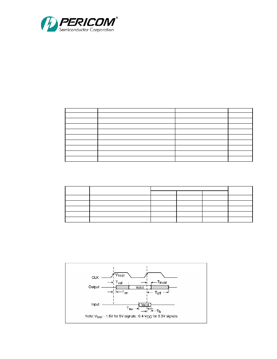
PI7C21P100
2-PORT PCI-X BRIDGE
ADVANCE INFORMATION
Page 74 of 77
June 10, 2005 Revision 1.06
10
ELECTRICAL INFORMATION
10.1
MAXIMUM RATINGS
Stresses greater than those listed under MAXIMUM RATINGS may cause permanent damage
to the device. This is a stress rating only and functional operation of the device at these or any
conditions above those indicated in the operational sections of this specification is not
implied. Exposure to absolute maximum rating conditions for extended periods of time may
affect reliability.
SYMBOL PARAMETER
RATING
UNITS
V
DD
Core logic power supply
TBD
V
V
DD2
I/O power supply voltage
TBD
V
V
IN
Input voltage
TBD
V
V
OUT
Output voltage
TBD
V
T
A
Ambient operating temperature
0 to 70
°C
T
J
Maximum junction temperature
125
°C
T
STG
Storage temperature
-55 to 125
°C
P
WC
Worst case power dissipation
TBD
W
I
OUT
Short circuit output current
TBD
mA
10.2
DC SPECIFICATIONS
RATING
SYMBOL PARAMETER
min typ max
UNITS
V
DD
Core logic power supply
2.3
2.5
2.7
V
V
DD2
I/O power supply voltage
3.0
3.3
3.6
V
V
IH
Input High voltage
2.0
-
V
DDI
* + 0.5
V
V
IL
Input Low voltage
-0.3
-
0.3 V
DDI
*
V
C
IN
Input pin capacitance
-
-
8.0
pF
*
V
DDI
is in reference to the power supply of the input device.
10.3
AC SPECIFICATIONS
Figure 10-1 PCI SIGNAL TIMING MEASUREMENTS
PI7C21P100
2-PORT PCI-X BRIDGE
ADVANCE INFORMATION
Page 75 of 77
June 10, 2005 Revision 1.06
Table 10-1 AC TIMING SPECIFICATIONS PCI-X MODE
PCI-X 133
PCI-X 100
PCI-X 66
Symbol Parameter
min max min
max min max
Units
Tsu
Input setup time to CLK bussed
signals
1.2 - 1.2 - 1.7 - ns
Tsu(ptp)
Input setup time to CLK point-to-
point signals
1.2 - 1.2 - 1.7 - ns
Th
Input signal hold time from CLK
0.5
-
0.5
-
0.5
-
ns
Tval
CLK to signal valid delay bussed
signals
0.7 3.8 0.7 3.8 0.7 3.8 ns
Tval(ptp)
CLK to signal valid delay point-
to-point signals
0.7 3.8 0.7 3.8 0.7 3.8 ns
Ton
Float
to
active
delay
0 - 0 - 0 - ns
Toff
Active
to
float
delay
- 7 - 7 - 7 ns
Table 10-2 AC TIMING SPECIFICATIONS CONVENTIONAL PCI MODE
PCI 66
PCI 33
Symbol Parameter
min max
min
max
Units
Tsu
Input setup time to CLK bussed
signals
3 - 7 -
ns
Tsu(ptp)
Input setup time to CLK point-to-
point signals
5 -
10,
12
-
ns
Th
Input signal hold time from CLK
0
-
0
-
ns
Tval
CLK to signal valid delay bussed
signals
2 6 2 11
ns
Tval(ptp)
CLK to signal valid delay point-
to-point signals
2 6 2 12
ns
Ton
Float to active delay
2
-
2
-
ns
Toff
Active to float delay
-
14
-
14
ns
10.4
POWER CONSUMPTION
RATING
PARAMETER
min typ max
UNITS
Power dissipation for V
DD
(2.5V)
1.33 W
Power dissipation for V
DD2
(3.3V)
0.46 W
*Running at 133MHz
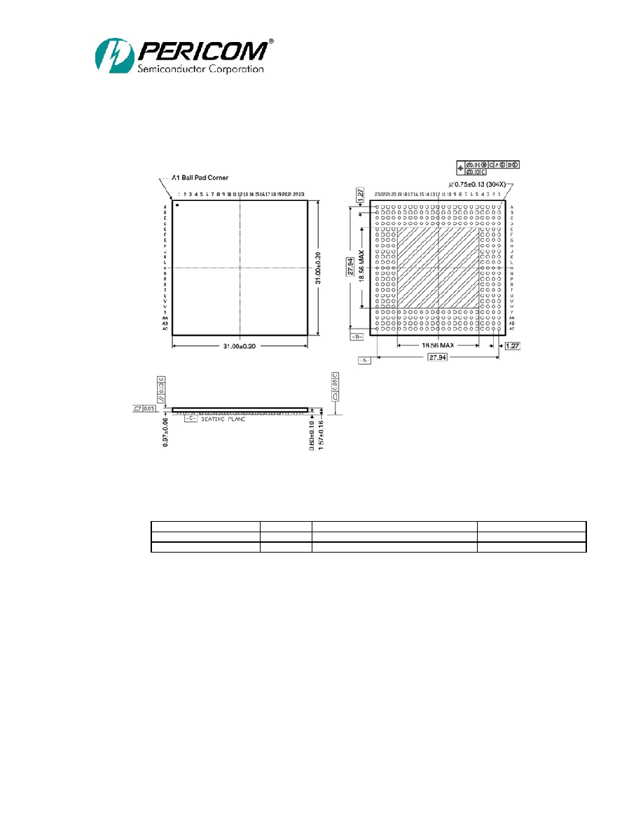
PI7C21P100
2-PORT PCI-X BRIDGE
ADVANCE INFORMATION
Page 76 of 77
June 10, 2005 Revision 1.06
11
MECHANICAL INFORMATION
Figure 11-1 PACKAGE DIAGRAM 31 X 31mm 304-PIN CSBGA
12
ORDERING INFORMATION
PART NUMBER
SPEED
PIN PACKAGE
TEMPERATURE
PI7C21P100NH
133MHz
304-PINS CSGA
0°C TO 85°C
PI7C21P100NH
133MHz
Pb-free & Green, 304-PINS - CSBGA
0°C TO 85°C

PI7C21P100
2-PORT PCI-X BRIDGE
ADVANCE INFORMATION
Page 77 of 77
June 10, 2005 Revision 1.06
NOTES: