Äîêóìåíòàöèÿ è îïèñàíèÿ www.docs.chipfind.ru

09/18/00 Rev 1.1
PI7C7100
3-Port
PCI Bridge
The Complete Interface Solution
2380 Bering Drive, San Jose, California 95131
Telephone: 1-877-PERICOM, (1-877-737-4266)
Fax: (408) 435-1100, E-mail: nolimits@pericom.com
Internet: http://www.pericom.com
© 2000 Pericom Semiconductor Corporation
Pericom Semiconductor Corporation
Rev 1.1

ii
12345678901234567890123456789012123456789012345678901234567890121234567890123456789012345678901212345678901234567890123456789012123456
12345678901234567890123456789012123456789012345678901234567890121234567890123456789012345678901212345678901234567890123456789012123456
PI7C7100
3-Port PCI Bridge
ADVANCE INFORMATION
09/18/00 Rev 1.1
LIFE SUPPORT POLICY
Pericom Semiconductor Corporation's products are not authorized for use as critical components in life support devices or
systems unless a specific written agreement pertaining to such intended use is executed between the manufacturer and an
officer of PSC.
1.Life support devices or systems are devices or systems which:
a) are intended for surgical implant into the body or
b) support or sustain life and whose failure to perform, when properly used in accordance with instructions for use provided
in the labeling, can be reasonably expected to result in a significant injury to the user.
2. A critical component is any component of a life support device or system whose failure to perform can be reasonably
expected to cause the failure of the life support device or system, or to affect its safety or effectiveness.Pericom Semiconductor
Corporation reserves the right to make changes to its products or specifications at any time, without notice, in order to improve
design or performance and to supply the best possible product. Pericom Semiconductor does not assume any responsibility
for use of any circuitry described other than the circuitry embodied in a Pericom Semiconductor product. The Company makes
no representations that circuitry described herein is free from patent infringement or other rights of third parties which may
result from its use. No license is granted by implication or otherwise under any patent, patent rights or other rights, of Pericom
Semiconductor Corporation.
All other trademarks are of their respective companies.

iii
123456789012345678901234567890121234567890123456789012345678901212345678901234567890123456789012123456789012345678901234567890121234567
123456789012345678901234567890121234567890123456789012345678901212345678901234567890123456789012123456789012345678901234567890121234567
123456789012345678901234567890121234567890123456789012345678901212345678901234567890123456789012123456789012345678901234567890121234567
PI7C7100
3-Port PCI Bridge
ADVANCE INFORMATION
09/18/00 Rev 1.1
1.
Introduction/Product Features ............................................................................................................................... 1
2.
PI7C7100 Block Diagram ...................................................................................................................................... 3
3.
Signal Definitions ................................................................................................................................................... 4
3.1
Signal Types ............................................................................................................................................................ 4
3.2
Signals ...................................................................................................................................................................... 4
3.2.1
Primary Bus Interface Signals .................................................................................................................................. 4
3.2.2
Secondary Bus Interface Signals ............................................................................................................................. 6
3.2.3
Clock Signals ............................................................................................................................................................ 8
3.2.4
Miscellaneous Signals ............................................................................................................................................. 8
3.2.5
JTAG Boundary Scan Signals .................................................................................................................................. 9
3.2.6
Power and Ground .................................................................................................................................................... 9
3.3
PI7C7100 PBGA Pin Listing ..................................................................................................................................... 9
4.
PCI Bus Operation ................................................................................................................................................ 13
4.1
Types of Transactions ........................................................................................................................................... 13
4.2
Single Address Phase ............................................................................................................................................ 14
4.3
Device Select (DEVSEL#) Generation .................................................................................................................... 14
4.4
Data Phase ............................................................................................................................................................. 14
4.5
Write Transactions ................................................................................................................................................ 14
4.5.1
Posted Write Transactions .................................................................................................................................... 14
4.5.2
Memory Write and Invalidate Transactions .......................................................................................................... 15
4.5.3
Delayed Write Transactions .................................................................................................................................. 15
4.5.4
Write Transaction Address Boundaries ................................................................................................................ 16
4.5.5
Buffering Multiple Write Transactions .................................................................................................................. 16
4.5.6
Fast Back-to-Back Write Transactions .................................................................................................................. 16
4.6
Read Transactions ................................................................................................................................................. 17
4.6.1
Prefetchable Read Transactions ............................................................................................................................ 17
4.6.2
Non-prefetchable Read Transactions .................................................................................................................... 17
4.6.3
Read Pre-fetch Address Boundaries ...................................................................................................................... 17
4.6.4
Delayed Read Requests ......................................................................................................................................... 18
4.6.5
Delayed Read Completion with Target .................................................................................................................. 18
4.6.6
Delayed Read Completion on Initiator Bus ........................................................................................................... 18
4.7
Configuration Transactions ................................................................................................................................... 19
4.7.1
Type 0 Access to PI7C7100 ................................................................................................................................... 19
4.7.2
Type 1 to Type 0 Conversion ................................................................................................................................ 20
4.7.3
Type 1 to Type 1 Forwarding ................................................................................................................................ 21
4.7.4
Special Cycles ........................................................................................................................................................ 22
4.8
Transaction Termination ........................................................................................................................................ 22
4.8.1
Master Termination Initiated by PI7C7100 ............................................................................................................ 23
4.8.2
Master Abort Received by PI7C7100 ..................................................................................................................... 23
4.8.3
Target Termination Received by PI7C7100 ............................................................................................................ 24
4.8.3.1
Delayed Write Target Termination Response ....................................................................................................... 24
4.8.3.2 Posted Write Target Termination Response ......................................................................................................... 24
4.8.3.3 Delayed Read Target Termination Response ........................................................................................................ 25
4.8.4
Target Termination Initiated by PI7C7100 ............................................................................................................. 26
4.8.4.1 Target Retry ........................................................................................................................................................... 26
4.8.4.2 Target Disconnect .................................................................................................................................................. 27
Table of Contents

iv
12345678901234567890123456789012123456789012345678901234567890121234567890123456789012345678901212345678901234567890123456789012123456
12345678901234567890123456789012123456789012345678901234567890121234567890123456789012345678901212345678901234567890123456789012123456
PI7C7100
3-Port PCI Bridge
ADVANCE INFORMATION
09/18/00 Rev 1.1
4.8.4.3 Target Abort .......................................................................................................................................................... 27
4.9
Concurrent Mode Operation .................................................................................................................................. 27
5.
Address Decoding .................................................................................................................................................. 28
5.1
Address Ranges ..................................................................................................................................................... 28
5.2
I/O Address Decoding ........................................................................................................................................... 28
5.2.1
I/O Base and Limit Address Registers ................................................................................................................... 28
5.2.2
ISA Mode ............................................................................................................................................................... 29
5.3
Memory Address Decoding ................................................................................................................................... 29
5.3.1
Memory-Mapped I/O Base and Limit Address Registers ...................................................................................... 30
5.3.2
Prefetchable Memory Base and Limit Address Registers ...................................................................................... 30
5.4
VGA Support .......................................................................................................................................................... 31
5.4.1
VGA Mode ............................................................................................................................................................. 31
5.4.2
VGA Snoop Mode .................................................................................................................................................. 31
6.
Transaction Ordering ........................................................................................................................................... 32
6.1
Transactions Governed by Ordering Rules ........................................................................................................... 32
6.2
General Ordering Guidelines .................................................................................................................................. 32
6.3
Ordering Rules ....................................................................................................................................................... 33
6.4
Data Synchronization ............................................................................................................................................. 34
7.
Error Handling ...................................................................................................................................................... 35
7.1
Address Parity Errors ............................................................................................................................................. 35
7.2
Data Parity Errors ................................................................................................................................................... 35
7.2.1
Configuration Write Transactions to Configuration Space ................................................................................... 35
7.2.2
Read Transactions ................................................................................................................................................. 36
7.2.3
Delayed Write Transactions .................................................................................................................................. 36
7.2.4
Posted Write Transactions .................................................................................................................................... 38
7.3
Data Parity Error Reporting Summary .................................................................................................................... 39
7.4
System Error (SERR#) Reporting ........................................................................................................................... 45
8.
Exclusive Access ................................................................................................................................................... 46
8.1
Concurrent Locks ................................................................................................................................................... 46
8.2
Acquiring Exclusive Access across PI7C7100 ....................................................................................................... 46
8.3
Ending Exclusive Access ....................................................................................................................................... 47
9.
PCI Bus Arbitration .............................................................................................................................................. 48
9.1
Primary PCI Bus Arbitration ................................................................................................................................... 48
9.2
Secondary PCI Bus Arbitration ............................................................................................................................. 48
9.2.1
Secondary Bus Arbitration Using the Internal Arbiter .......................................................................................... 48
9.2.2
Secondary Bus Arbitration Using an External Arbiter ........................................................................................... 49
9.2.3
Bus Parking ............................................................................................................................................................ 49
10.
Clocks .................................................................................................................................................................... 50
10.1
Primary Clock Inputs .............................................................................................................................................. 50
10.2
Secondary Clock Outputs ...................................................................................................................................... 50
11.
Reset ...................................................................................................................................................................... 51
11.1
Primary Interface Reset .......................................................................................................................................... 51
11.2
Secondary Interface Reset ..................................................................................................................................... 51
11.3
Chip Reset .............................................................................................................................................................. 51
12.
Supported Commands ............................................................................................................................................ 52
12.1
Primary Interface .................................................................................................................................................... 52
12.2
Secondary Interface ............................................................................................................................................... 54
13.
Configuration Registers ....................................................................................................................................... 55

v
123456789012345678901234567890121234567890123456789012345678901212345678901234567890123456789012123456789012345678901234567890121234567
123456789012345678901234567890121234567890123456789012345678901212345678901234567890123456789012123456789012345678901234567890121234567
123456789012345678901234567890121234567890123456789012345678901212345678901234567890123456789012123456789012345678901234567890121234567
PI7C7100
3-Port PCI Bridge
ADVANCE INFORMATION
09/18/00 Rev 1.1
13.1
Config Register 1 .................................................................................................................................................... 55
13.2
Config Register 2 .................................................................................................................................................... 56
13.2.1
Config Register 1 or 2:Vendor ID Register (read only, bit 15-0; offset 00h) .......................................................... 57
13.2.2
Config Register 1: Device ID Register (read only, bit 31-16; offset 00h) ............................................................... 57
13.2.3
Config Register 2: Device ID Register (read only, bit 31-16; offset 00h) ............................................................... 57
13.2.4
Config Register 1: Command Register (bit 15-0; offset 04h) .................................................................................. 57
13.2.5
Config Register 2: Command Register (bit 15-0; offset 04h) .................................................................................. 58
13.2.6
Config Register 1 or 2: Status Register (for primary bus, bit 31-16; offset 04h) ..................................................... 59
13.2.7
Config Register 1 or 2: Revision ID Register (read only, bit 7-0; offset 08h) ......................................................... 60
13.2.8
Config Register 1 or 2: Class Code Register (read only, bit 31-8; offset 08h) ........................................................ 60
13.2.9
Config Register 1 or 2: Cache Line Size Register (read/write, bit 7-0; offset 0Ch) ................................................. 60
13.2.10 Config Register 1: Primary Latency Timer Register (read/write, bit 15-8; offset 0Ch) ............................................ 60
13.2.11 Config Register 2: Primary Latency Timer Register (read/write, bit 15-8; offset 0Ch) ............................................ 60
13.2.12 Config Register 1: Header Type Register (read only, bit 23-16; offset 0Ch) .......................................................... 60
13.2.13 Config Register 2: Header Type Register (read only, bit 23-16; offset 0Ch) .......................................................... 60
13.2.14 Config Register 1: Primary Bus Number Register (read/write, bit 7-0; offset 18h) ................................................. 60
13.2.15 Config Register 2: Primary Bus Number Register (read/write, bit 7-0; offset 18h) ................................................. 60
13.2.16 Config Register 1 or 2: Secondary Bus Number Register (read/write, bit 15-8; offset 18h) ................................... 60
13.2.17 Config Register 1 or 2: Subordinate Bus Number Register (read/write, bit 23-16; offset 18h) ............................... 60
13.2.18 Config Register 1 or 2: Secondary Latency Timer (read/write, bit 31-24; offset 18h) ............................................ 60
13.2.19 Config Register 1 or 2: I/O Base Register (read/write, bit 7-0; offset 1Ch) ............................................................ 60
13.2.20 Config Register 1 or 2: I/O Limit Register (read/write, bit 15-8; offset 1Ch) ........................................................... 60
13.2.21 Config Register 1 or 2: Secondary Status Register (bit 31-16; offset 1Ch) ............................................................ 61
13.2.22 Config Register 1 or 2: Memory Base Register (read/write, bit 15-0; offset 20h) ................................................... 62
13.2.23 Config Register 1 or 2: Memory Limit Register (read/write, bit 31:16; offset 20h) ................................................. 62
13.2.24 Config Register 1 or 2: Prefetchable Memory Base Register (read/write, bit 15-0;offset 24h) ............................... 62
13.2.25 Config Register 1 or 2: Prefetchable Memory Limit Register (read/write, bit 31-16; offset 24h) ............................ 62
13.2.26 Config Register 1 or 2: I/O Base Address Upper 16 Bits Register (read/write, bit 15-0; offset 30h) ...................... 62
13.2.27 Config Register 1 or 2: I/O Limit Address Upper 16 Bits Register (read/write, bit 31-16; offset 30h) .................... 62
13.2.28 Config Register 1 or 2: Subsystem Vendor ID (read/write, bit 15-0; offset 34h) .................................................... 62
13.2.29 Config Register 1 or 2: Subsystem ID (read/write, bit 31-16; offset 34h) ............................................................... 62
13.2.30 Config Register 1 or 2: Interrupt Pin Register (read only, bit 15-8; offset 3Ch) ..................................................... 62
13.2.31 Config Register 1 or 2: Bridge Control Register (bit 31-16; offset 3Ch) ................................................................. 63
13.2.32 Config Register 1 or 2: Diagnostic/Chip Control Register (bit 15-0; offset 40h) .................................................... 64
13.2.33 Config Register 1 or 2: Arbiter Control Register (bit 31-16; offset 40h) ................................................................. 64
13.2.34 Config Register 1: Primary Prefetchable Memory Base Register (Read/Write, bit 15-0; offset 44h) ..................... 65
13.2.35 Config Register 2: Primary Prefetchable Memory Base Register (Read/Write, bit 15-0; offset 44h) ..................... 65
13.2.36 Config Register 1: Primary Prefetchable Memory Limit Register (Read/Write, bit 31-16; offset 44h) .................... 65
13.2.37 Config Register 2: Primary Prefetchable Memory Limit Register (Read/Write, bit 31-16; offset 44h) .................... 65
13.2.38 Config Register 1 or 2: P_SERR# Event Disable Register (bit 7-0; offset 64h) ...................................................... 65
13.2.39 Config Register 1: Secondary Clock Control Register (bit 15-0; offset 68h) .......................................................... 66
13.2.40 Config Register 2: Secondary Clock Control Register (bit 15-0; offset 68h) .......................................................... 66
13.2.41 Config Register 1 or 2: Non-Posted Memory Base Register (read/write, bit 15-0; offset 70h) .............................. 67
13.2.42 Config Register 1 or 2: Non-Posted Memory Limit Register (read/write, bit 31-16; offset 70h) ............................. 67
13.2.43 Config Register 1: Port Option Register (bit 15-0; offset 74h) ............................................................................... 67
13.2.44 Config Register 2: Port Option Register (bit 15-0; offset 74h) ............................................................................... 68
13.2.45 Config Register 1 or 2: Master Timeout Counter Register (read/write, bit 31-16; offset 74h) ................................ 69
13.2.46 Config Register 1 or 2: Retry Counter Register (read/write, bit 31-0; offset 78h) .................................................. 69
13.2.47 Config Register 1 or 2: Sampling Timer Register (read/write, bit 31-0; offset 7Ch) ................................................ 69
13.2.48 Config Register 1 or 2: Successful I/O Read Count Register (read/write, bit 31-0; offset 80h) ............................. 69

vi
12345678901234567890123456789012123456789012345678901234567890121234567890123456789012345678901212345678901234567890123456789012123456
12345678901234567890123456789012123456789012345678901234567890121234567890123456789012345678901212345678901234567890123456789012123456
PI7C7100
3-Port PCI Bridge
ADVANCE INFORMATION
09/18/00 Rev 1.1
13.2.49 Config Register 1 or 2: Successful I/O Write Count Register (read/write, bit 31-0; offset 84h) ............................. 69
13.2.50 Config Register 1 or 2: Successful Memory Read Count Register (read/write, bit 31-0; offset 88h) ..................... 69
13.2.51 Config Register 1 or 2: Successful Memory Write Count Register (read/write, bit 31-0; offset 8Ch) .................... 69
13.2.52 Config Register 1: Primary Successful I/O Read Count Register (read/write, bit 31-0; offset 90h) ....................... 69
13.2.53 Config Register 1: Primary Successful I/O Write Count Register (read/write, bit 31-0; offset 94h) ....................... 69
13.2.54 Config Register 1: Primary Successful Memory Read Count Register (read/write, bit 31-0; offset 98h) ............... 69
13.2.55 Config Register 1: Primary Successful Memory Write Count Register (read/write, bit 31-0; offset 9Ch) .............. 69
14.
Bridge Behavior .................................................................................................................................................... 70
14.1
Bridge Actions for Various Cycle Types ............................................................................................................... 70
14.2
Transaction Ordering ............................................................................................................................................. 70
14.3
Abnormal Termination (Initiated by Bridge Master) ............................................................................................. 71
14.3.1
Master Abort ......................................................................................................................................................... 71
14.3.2
Parity and Error Reporting ..................................................................................................................................... 71
14.3.3
Reporting Parity Errors ........................................................................................................................................... 71
14.3.4
Secondary IDSEL mapping .................................................................................................................................... 71
15.
IEEE 1149.1 Compatible JTAG Controller ........................................................................................................... 72
15.1
Boundary Scan Architecture ................................................................................................................................. 72
15.1.1
TAP Pins ................................................................................................................................................................ 72
15.1.2
Instruction Register ............................................................................................................................................... 72
15.2
Boundary Scan Instruction Set .............................................................................................................................. 73
15.3
TAP Test Data Registers ....................................................................................................................................... 74
15.4
Bypass Register ..................................................................................................................................................... 74
15.5
Boundary-Scan Register ......................................................................................................................................... 74
15.6
TAP Controller ....................................................................................................................................................... 74
16.
Electrical and Timing Specifications .................................................................................................................... 79
16.1
Maximum Ratings ................................................................................................................................................... 79
16.2
3.3V DC Specifications ........................................................................................................................................... 79
16.3
3.3V AC Specifications ........................................................................................................................................... 80
16.4
Primary and Secondary buses at 33 MHz clock timing .......................................................................................... 80
16.5
Power Consumption ............................................................................................................................................... 80
17.
256-Pin PBGA Package ........................................................................................................................................... 81
17.1
Part Number Ordering Information ........................................................................................................................ 81

vii
123456789012345678901234567890121234567890123456789012345678901212345678901234567890123456789012123456789012345678901234567890121234567
123456789012345678901234567890121234567890123456789012345678901212345678901234567890123456789012123456789012345678901234567890121234567
123456789012345678901234567890121234567890123456789012345678901212345678901234567890123456789012123456789012345678901234567890121234567
PI7C7100
3-Port PCI Bridge
ADVANCE INFORMATION
09/18/00 Rev 1.1
List of Figures
1-1.
PI7C7100 on the System Board .................................................................................................................................... 2
1-2.
PI7C7100 in Redundant Applications .......................................................................................................................... 2
1-3.
PI7C7100 on Network Switching Hub .......................................................................................................................... 2
2-1.
PI7C7100 Block Diagram .............................................................................................................................................. 3
9-1.
Secondary Arbiter Example ....................................................................................................................................... 48
15-1. Test Access Port Block Diagram ............................................................................................................................... 72
16-1. PCI Signal Timing Measurement Conditions ............................................................................................................ 80
17-1. 256-Pin PBGA Package Drawing ................................................................................................................................ 81
List of Tables
4-1.
PCI Transaction ......................................................................................................................................................... 13
4-2.
Write Transaction Forwarding .................................................................................................................................. 14
4-3.
Write Transaction Disconnect Address Boundaries ................................................................................................ 16
4-4.
Read Pre-fetch Address Boundaries ......................................................................................................................... 17
4-5.
Read Transaction Pre-fetching .................................................................................................................................. 18
4-6.
Device Number to IDSEL S1_AD or S2_AD Pin Mapping ....................................................................................... 21
4-7.
Delayed Write Target Termination Response ........................................................................................................... 24
4-8.
Responses to Posted Write Target Termination ....................................................................................................... 25
4-9.
Responses to Delayed Read Target Termination ...................................................................................................... 25
6-1.
Summary of Tranaction Ordering .............................................................................................................................. 33
7-1.
Setting the Primary Interface Detected Parity Error Bit ............................................................................................. 39
7-2.
Setting the Secondary Interface Detected Parity Error Bit ........................................................................................ 40
7-3.
Setting the Primary Interface Data Parity Detected Bit .............................................................................................. 40
7-4.
Setting the Secondary InterfaceData Parity Detected Bit ......................................................................................... 41
7-5.
Assertion of P_PERR# ............................................................................................................................................... 42
7-6.
Assertion of S_PERR# ............................................................................................................................................... 43
7-7.
Assertion of P_SERR# for Data Parity Errors ........................................................................................................... 44
15-1. TAP Pins .................................................................................................................................................................... 73
15-2. JTAG Boundary Register Order ................................................................................................................................ 75

viii
12345678901234567890123456789012123456789012345678901234567890121234567890123456789012345678901212345678901234567890123456789012123456
12345678901234567890123456789012123456789012345678901234567890121234567890123456789012345678901212345678901234567890123456789012123456
PI7C7100
3-Port PCI Bridge
ADVANCE INFORMATION
09/18/00 Rev 1.1
Appendix A - Timing Diagrams
1.
Configuration Read Transaction ................................................................................................................................. A-3
2. Configuration Write Transaction ................................................................................................................................ A-3
3.
Type 1 to Type 0 Configuration Read Transaction (P
S) ...................................................................................... A-3
4. Type 1 to Type 0 Configuration Write Transaction (P
S) ..................................................................................... A-4
5. Upstream Type 1 to Special Cycle Transaction (S
P) ............................................................................................. A-4
6.
Downstream Type 1 to Special Cycle Transaction (P
S) ........................................................................................ A-5
7. Downstream Type 1 to Type 1 Configuration Read Transaction (P
S) .................................................................. A-5
8. Downstream Type 1 to Type 1 Configuration Write Transaction (P
S) ................................................................. A-6
9. Upstream Delayed Burst Memory Read Transaction (S
P) ................................................................................... A-6
10. Downstream Delayed Burst Memory Read Transaction (P
S) .............................................................................. A-7
11. Downstream Delayed Memory Read Transaction (P/33MHz
S/33MHz) ............................................................... A-7
12. Downstream Delayed Memory Read Transaction (S2/33MHz
S1/33MHz) ........................................................... A-8
13. Downstream Delayed Memory Read Transaction (S1/33MHz
S2/33MHz) ........................................................... A-8
14. Upstream Delayed Memory Read Transaction (S/33MHz
P/33MHz) ................................................................... A-9
15. Downstream Posted Memory Write Transaction (P/33MHz
S/33MHz) ................................................................ A-9
16. Downstream Posted Memory Write Transaction (S2/33MHz
S1/33MHz) ........................................................... A-10
17. Downstream Posted Memory Write Transaction (S1/33MHz
S2/33MHz) ........................................................... A-10
18. Upstream Posted Memory Write Transaction (S/33MHz
P/33MHz) ................................................................... A-11
19. Downstream Flow-Through Posted Memory Write Transaction (P/33MHz
S/33MHz) ........................................ A-11
20. Downstream Flow-Through Posted Memory Write Transaction (S2/33MHz
S1/33MHz) .................................... A-12
21. Downstream Flow-Through Posted Memory Write Transaction (S1/33MHz
S2/33MHz) .................................... A-12
22. Upstream Flow-Through Posted Memory Write Transaction (S/33MHz
P/33MHz) ............................................ A-13
23. Downstream Delayed I/O Read Transaction (P
S) ............................................................................................... A-13
24. Downstream Delayed I/O Read Transaction (S2/33MHz
S1/33MHz) .................................................................. A-14
25. Downstream Delayed I/O Read Transaction (S1/33MHz
S2/33MHz) .................................................................. A-14
26. Downstream Delayed I/O Read Transaction (S/33MHz
P/33MHz) ...................................................................... A-15
27. Downstream Delayed I/O Write Transaction (P
S) .............................................................................................. A-15
28. Downstream Delayed I/O Write Transaction (S2/33MHz
S1/33MHz) ................................................................. A-16
29. Downstream Delayed I/O Write Transaction (S1/33MHz
S2/33MHz) ................................................................. A-16
30. Upstream Delayed I/O Write Transaction (S
P) ................................................................................................... A-17
Appendix B - Evaluation Board User's Manual
General Information ........................................................................................................................................................... B-3
Frequently Asked Questions ............................................................................................................................................ B-5
Appendix C - Three-Port PCI Bridge Evaluation Board Schematics
PCI Chip ............................................................................................................................................................................. C-3
PCI Edge Connector .......................................................................................................................................................... C-4
Secondary 1 PCI Bus ......................................................................................................................................................... C-5
Secondary 2 PCI Bus ......................................................................................................................................................... C-6
Top View ............................................................................................................................................................................ C-7
Appendix D - Representatives and Distributors

1
09/18/00 Rev 1.1
123456789012345678901234567890121234567890123456789012345678901212345678901234567890123456789012123456789012345678901234567890121234567
123456789012345678901234567890121234567890123456789012345678901212345678901234567890123456789012123456789012345678901234567890121234567
PI7C7100
3-Port PCI Bridge
ADVANCE INFORMATION
Product Features
· 32-bit Primary & two Secondary Ports run up to 33 MHz
· All three ports compliant with the PCI Local Bus
Specification, Revision 2.1
· Compliant with PCI-to-PCI Bridge Architecture Specification, Revision 1.0.
- All I/O and memory commands
- Type 1 to Type 0 configuration conversion
- Type 1 to Type 1 configuration forwarding
- Type 1 configuration-write to special cycle conversion
· Concurrent primary to secondary bus operation and independent intra-secondary port
channel to reduce traffic on the primary port
· Provides internal arbitration for two sets of eight secondary bus masters
- Programmable 2-level priority arbiter
- Disable control for use of external arbiter
· Supports posted write buffers on all directions
· Three 128 byte FIFOs for delay transactions
· Three 128 byte FIFOs for posted memory transactions
· Enhanced address decoding
- 32-bit I/O address range
- 32-bit memory-mapped I/O address range
- VGA addressing and VGA palette snooping
- ISA-aware mode for legacy support in the first 64KB
of I/O address range
· Interrupt Handling
- PCI interrupts are routed through an external interrupt concentrator
· Supports system transaction ordering rules
· Hot-plug support on secondary buses
- 3-State control of output buffers
· IEEE 1149.1 JTAG interface support
· 3.3V core; 3.3V PCI I/O interface with 5V I/O Tolerant
· 256-pin plastic BGA package
Product Description
PI7C7100 is the first triple port PCI-to-PCI Bridge device designed to be fully compliant with the 32-bit,
33 MHz implementation of the
PCI Local Bus Specification, Revision 2.1. PI7C7100 supports only
synchronous bus transactions between devices on the primary 33 MHz bus and the secondary buses
operating at 33 MHz. The primary and the secondary buses can also operate in concurrent mode,
resulting in added increase in system performance. Concurrent bus operation off-loads and isolates
unnecessary traffic from the primary bus; thereby enabling a master and a target device on the same
secondary PCI bus to communicate even while the primary bus is busy.
1. Introduction
2
09/18/00 Rev 1.1
12345678901234567890123456789012123456789012345678901234567890121234567890123456789012345678901212345678901234567890123456789012123456
12345678901234567890123456789012123456789012345678901234567890121234567890123456789012345678901212345678901234567890123456789012123456
PI7C7100
3-Port PCI Bridge
ADVANCE INFORMATION
Figure 1-2. PI7C7100 in Redundant Application
Figure 1-1. PI7C7100 on the System Board
S1 PCI Bus
S2 PCI Bus
PI7C7100
CPU
NB
Slot
Slot
System
Memory
PCI
Device
PCI
Device
PI7C7100
System Primary
PCI Bus
PI7C7100
S1 PCI Bus
Master Controller
Redundant Controller
S2 PCI Bus
System Primary
PCI Bus
S1
S1
S2
S2
Figure 1-3. PI7C7100 on Network Switching Hub
CPU
PCI Bus 32/33
PI7C7100
PCI Bus 32/33
Core
Logic
L2
Cache
I/O Daughter
Board to
Isolate Traffic
PI7C7100
PI7C7100
Fast
Ethernet
Internal
Slot
3
09/18/00 Rev 1.1
123456789012345678901234567890121234567890123456789012345678901212345678901234567890123456789012123456789012345678901234567890121234567
123456789012345678901234567890121234567890123456789012345678901212345678901234567890123456789012123456789012345678901234567890121234567
PI7C7100
3-Port PCI Bridge
ADVANCE INFORMATION
Configuration
Register #1
Arbiter
Arbiter
Secondary
Interface B
Secondary
Interface A
Secondary
PCI Bus A
Transaction
Queue #1
Transaction
Queue #2
Transaction
Queue #3
Configuration
Register #2
Primary
PCI Bus
Secondary
PCI Bus B
Primary
Interface
2. PI7C7100 Block Diagram
Figure 2-1. PI7C7100 Block Diagram

4
09/18/00 Rev 1.1
12345678901234567890123456789012123456789012345678901234567890121234567890123456789012345678901212345678901234567890123456789012123456
12345678901234567890123456789012123456789012345678901234567890121234567890123456789012345678901212345678901234567890123456789012123456
PI7C7100
3-Port PCI Bridge
ADVANCE INFORMATION
e
p
y
T
l
a
n
g
i
S
n
o
i
t
p
i
r
c
s
e
D
I
P
)
t
n
a
r
e
l
o
t
V
5
,
V
3
.
3
(
t
u
p
n
I
I
C
P
U
I
P
p
u
-
ll
u
p
k
a
e
w
h
t
i
w
)
t
n
a
r
e
l
o
t
V
5
,
V
3
.
3
(
t
u
p
n
I
I
C
P
B
P
)
t
n
a
r
e
l
o
t
V
5
,
V
3
.
3
(
l
a
n
o
i
t
c
e
r
i
d
i
b
e
t
a
t
s
-
3
I
C
P
O
P
)
V
3
.
3
(
t
u
p
t
u
O
I
C
P
S
T
S
P
e
l
c
y
c
e
n
o
r
o
f
e
v
i
t
c
a
n
i
n
e
v
i
r
d
e
b
t
s
u
m
h
c
i
h
w
l
a
n
g
i
s
W
O
L
e
v
i
t
c
A
(
l
a
n
o
i
t
c
e
r
i
d
i
b
e
t
a
t
s
-
3
d
e
n
i
a
t
s
u
S
I
C
P
)
e
n
il
l
a
n
g
i
s
d
e
r
a
h
s
a
n
o
e
c
n
a
m
r
o
f
r
e
p
H
G
I
H
e
r
u
s
n
e
o
t
d
e
t
a
t
s
-
3
g
n
i
e
b
e
r
o
f
e
b
S
T
P
t
u
p
t
u
O
e
t
a
t
s
-
3
I
C
P
D
O
P
d
e
t
a
t
s
-
3
r
o
)
e
t
a
t
s
e
v
i
t
c
a
(
W
O
L
s
e
v
i
r
d
r
e
h
t
i
e
h
c
i
h
w
t
u
p
t
u
O
I
C
P
I
C
t
u
p
n
I
S
O
M
C
U
I
C
p
u
-
ll
u
p
k
a
e
w
h
t
i
w
t
u
p
n
I
S
O
M
C
D
I
C
n
w
o
d
-
ll
u
p
k
a
e
w
h
t
i
w
t
u
p
n
I
S
O
M
C
O
T
C
t
u
p
t
u
O
e
t
a
t
s
-
3
S
O
M
C
3. Signal Definitions
3.1 Signal Types
e
m
a
N
#
n
i
P
e
p
y
T
n
o
i
t
p
i
r
c
s
e
D
]
0
:
1
3
[
D
A
_
P
,
8
V
,
8
W
,
8
Y
,
7
W
,
7
Y
,
0
1
W
,
9
W
,
9
Y
,
8
U
,
1
1
U
,
1
1
V
,
1
1
Y
,
0
1
V
,
6
1
V
,
2
1
V
,
2
1
W
,
2
1
Y
,
7
1
W
,
6
1
Y
,
6
1
W
,
8
1
Y
,
8
1
W
,
8
1
U
,
7
1
Y
,
0
2
U
,
9
1
Y
,
9
1
W
,
9
1
U
7
1
R
,
7
1
T
,
0
2
Y
,
0
2
V
B
P
.
a
t
a
D
/
s
s
e
r
d
d
A
y
r
a
m
i
r
P
s
i
s
s
e
r
d
d
A
.
s
u
b
a
t
a
d
d
n
a
s
s
e
r
d
d
a
d
e
x
e
l
p
i
t
l
u
M
n
e
h
w
d
il
a
v
d
n
a
e
l
b
a
t
s
s
i
a
t
a
d
e
t
i
r
W
.
n
o
i
t
r
e
s
s
a
#
E
M
A
R
F
_
P
y
b
d
e
t
a
c
i
d
n
i
s
i
#
Y
D
R
T
_
P
n
e
h
w
d
il
a
v
d
n
a
e
l
b
a
t
s
s
i
a
t
a
d
d
a
e
r
d
n
a
d
e
t
r
e
s
s
a
s
i
#
Y
D
R
I
_
P
d
n
a
#
Y
D
R
I
_
P
h
t
o
b
n
e
h
w
s
e
g
d
e
k
c
o
l
c
g
n
i
s
i
r
n
o
d
e
r
r
e
f
s
n
a
r
t
s
i
a
t
a
D
.
d
e
t
r
e
s
s
a
d
il
a
v
a
o
t
D
A
_
P
s
e
v
i
r
d
0
0
1
7
C
7
I
P
,
e
l
d
i
s
u
b
g
n
i
r
u
D
.
d
e
t
r
e
s
s
a
e
r
a
#
Y
D
R
T
_
P
.
d
e
t
r
e
s
s
a
s
i
#
T
N
G
_
P
n
e
h
w
l
e
v
e
l
c
i
g
o
l
]
0
:
3
[
E
B
C
_
P
9
1
V
,
6
1
U
,
2
1
U
,
9
V
B
P
.
s
e
l
b
a
n
E
e
t
y
B
/
d
n
a
m
m
o
C
y
r
a
m
i
r
P
e
t
y
b
d
n
a
d
l
e
i
f
d
n
a
m
m
o
c
d
e
x
e
l
p
i
t
l
u
M
e
p
y
t
n
o
i
t
c
a
s
n
a
r
t
e
h
t
s
e
v
i
r
d
r
o
t
a
i
t
i
n
i
e
h
t
,
e
s
a
h
p
s
s
e
r
d
d
a
g
n
i
r
u
D
.
d
l
e
i
f
e
l
b
a
n
e
a
t
a
d
g
n
i
r
u
d
s
e
l
b
a
n
e
e
t
y
b
e
h
t
s
e
v
i
r
d
r
o
t
a
i
t
i
n
i
e
h
t
t
a
h
t
r
e
t
f
A
.
s
n
i
p
e
s
e
h
t
n
o
l
e
v
e
l
c
i
g
o
l
d
il
a
v
a
o
t
]
0
:
3
[
E
B
C
_
P
s
e
v
i
r
d
0
0
1
7
C
7
I
P
,
e
l
d
i
s
u
b
g
n
i
r
u
D
.
s
e
s
a
h
p
.
d
e
t
r
e
s
s
a
s
i
#
T
N
G
_
P
n
e
h
w
R
A
P
_
P
5
1
U
B
P
.
y
t
i
r
a
P
y
r
a
m
i
r
P
d
n
a
,
]
0
:
3
[
E
B
C
_
P
,
]
0
:
1
3
[
D
A
_
P
s
s
o
r
c
a
n
e
v
e
s
i
y
t
i
r
a
P
d
n
a
d
il
a
v
s
i
d
n
a
t
u
p
n
i
n
a
s
i
R
A
P
_
P
.
)
s
'
1
'
f
o
r
e
b
m
u
n
n
e
v
e
n
a
.
e
.
i
(
R
A
P
_
P
f
o
n
o
i
t
r
e
s
s
a
y
b
d
e
t
a
c
i
d
n
i
(
e
s
a
h
p
s
s
e
r
d
d
a
e
h
t
r
e
t
f
a
e
l
c
y
c
e
n
o
e
l
b
a
t
s
t
u
p
n
i
n
a
s
i
R
A
P
_
P
,
s
e
s
a
h
p
a
t
a
d
e
t
i
r
w
r
o
F
.
y
t
i
r
a
p
s
s
e
r
d
d
a
r
o
f
)
#
E
M
A
R
F
_
P
,
e
s
a
h
p
a
t
a
d
d
a
e
r
r
o
F
.
d
e
t
r
e
s
s
a
s
i
#
Y
D
R
I
_
P
r
e
t
f
a
k
c
o
l
c
e
n
o
d
il
a
v
s
i
d
n
a
.
d
e
t
r
e
s
s
a
s
i
#
Y
D
R
T
_
P
r
e
t
f
a
k
c
o
l
c
e
n
o
d
il
a
v
s
i
d
n
a
t
u
p
t
u
o
n
a
s
i
R
A
P
_
P
g
n
i
r
u
D
.
d
e
t
a
t
s
-
3
e
r
a
s
e
n
il
D
A
P
e
h
t
r
e
t
f
a
e
l
c
y
c
e
n
o
d
e
t
a
t
s
-
i
r
t
s
i
R
A
P
_
P
l
a
n
g
i
S
s
i
#
T
N
G
_
P
n
e
h
w
l
e
v
e
l
c
i
g
o
l
d
il
a
v
a
o
t
R
A
P
P
s
e
v
i
r
d
0
0
1
7
C
7
I
P
,
e
l
d
i
s
u
b
.
d
e
t
r
e
s
s
a
#
E
M
A
R
F
_
P
3
1
W
S
T
S
P
.
)
W
O
L
e
v
i
t
c
A
(
E
M
A
R
F
y
r
a
m
i
r
P
o
t
n
o
i
t
c
a
s
n
a
r
t
a
f
o
r
o
t
a
i
t
i
n
i
e
h
t
y
b
n
e
v
i
r
D
f
o
n
o
i
t
r
e
s
s
a
-
e
d
e
h
T
.
s
s
e
c
c
a
n
a
f
o
n
o
i
t
a
r
u
d
d
n
a
g
n
i
n
n
i
g
e
b
e
h
t
e
t
a
c
i
d
n
i
e
r
o
f
e
B
.
r
o
t
a
i
t
i
n
i
e
h
t
y
b
d
e
t
s
e
u
q
e
r
e
s
a
h
p
a
t
a
d
l
a
n
i
f
e
h
t
s
e
t
a
c
i
d
n
i
#
E
M
A
R
F
_
P
.
e
l
c
y
c
e
n
o
r
o
f
e
t
a
t
s
d
e
t
r
e
s
s
a
-
e
d
a
o
t
n
e
v
i
r
d
s
i
t
i
,
d
e
t
a
t
s
-
3
g
n
i
e
b
3.2 Signals
(Note: Signal name that ends with character `#' is active LOW.)
3.2.1 Primary Bus Interface Signals

5
09/18/00 Rev 1.1
123456789012345678901234567890121234567890123456789012345678901212345678901234567890123456789012123456789012345678901234567890121234567
123456789012345678901234567890121234567890123456789012345678901212345678901234567890123456789012123456789012345678901234567890121234567
PI7C7100
3-Port PCI Bridge
ADVANCE INFORMATION
e
m
a
N
#
n
i
P
e
p
y
T
n
o
i
t
p
i
r
c
s
e
D
#
Y
D
R
I
_
P
3
1
V
S
T
S
P
o
t
y
t
il
i
b
a
s
t
i
e
t
a
c
i
d
n
i
o
t
n
o
i
t
c
a
s
n
a
r
t
a
f
o
r
o
t
a
i
t
i
n
i
e
h
t
y
b
n
e
v
i
r
D
.
)
W
O
L
e
v
i
t
c
A
(
Y
D
R
I
y
r
a
m
i
r
P
t
o
n
s
i
t
i
,
e
s
a
h
p
a
t
a
d
a
n
i
d
e
t
r
e
s
s
a
e
c
n
O
.
e
d
i
s
y
r
a
m
i
r
p
e
h
t
n
o
e
s
a
h
p
a
t
a
d
t
n
e
r
r
u
c
e
t
e
l
p
m
o
c
d
e
t
r
e
s
s
a
-
e
d
a
o
t
n
e
v
i
r
d
s
i
t
i
,
d
e
t
a
t
s
-
3
g
n
i
e
b
e
r
o
f
e
B
.
e
s
a
h
p
a
t
a
d
f
o
d
n
e
l
i
t
n
u
d
e
t
r
e
s
s
a
-
e
d
.
e
l
c
y
c
e
n
o
r
o
f
e
t
a
t
s
#
Y
D
R
T
_
P
3
1
U
S
T
S
P
o
t
y
t
il
i
b
a
s
t
i
e
t
a
c
i
d
n
i
o
t
n
o
i
t
c
a
s
n
a
r
t
a
f
o
t
e
g
r
a
t
e
h
t
y
b
n
e
v
i
r
D
.
)
W
O
L
e
v
i
t
c
A
(
Y
D
R
T
y
r
a
m
i
r
P
t
o
n
s
i
t
i
,
e
s
a
h
p
a
t
a
d
a
n
i
d
e
t
r
e
s
s
a
e
c
n
O
.
e
d
i
s
y
r
a
m
i
r
p
e
h
t
n
o
e
s
a
h
p
a
t
a
d
t
n
e
r
r
u
c
e
t
e
l
p
m
o
c
d
e
t
r
e
s
s
a
-
e
d
a
o
t
n
e
v
i
r
d
s
i
t
i
,
d
e
t
a
t
s
-
3
g
n
i
e
b
e
r
o
f
e
B
.
e
s
a
h
p
a
t
a
d
f
o
d
n
e
l
i
t
n
u
d
e
t
r
e
s
s
a
-
e
d
.
e
l
c
y
c
e
n
o
r
o
f
e
t
a
t
s
#
L
E
S
V
E
D
_
P
4
1
Y
S
T
S
P
.
)
W
O
L
e
v
i
t
c
A
(
t
c
e
l
e
S
e
c
i
v
e
D
y
r
a
m
i
r
P
e
c
i
v
e
d
e
h
t
t
a
h
t
g
n
i
t
a
c
i
d
n
i
t
e
g
r
a
t
e
h
t
y
b
d
e
t
r
e
s
s
A
l
a
n
g
i
s
s
i
h
t
f
o
n
o
i
t
r
e
s
s
a
e
h
t
r
o
f
s
t
i
a
w
0
0
1
7
C
7
I
P
,
r
e
t
s
a
m
a
s
A
.
n
o
i
t
c
a
s
n
a
r
t
e
h
t
g
n
i
t
p
e
c
c
a
s
i
e
r
o
f
e
B
.
t
r
o
b
a
r
e
t
s
a
m
h
t
i
w
e
t
a
n
i
m
r
e
t
,
e
s
i
w
r
e
h
t
o
;
n
o
i
t
r
e
s
s
a
#
E
M
A
R
F
_
P
f
o
s
e
l
c
y
c
5
n
i
h
t
i
w
.
e
l
c
y
c
e
n
o
r
o
f
e
t
a
t
s
d
e
t
r
e
s
s
a
-
e
d
a
o
t
n
e
v
i
r
d
s
i
t
i
,
d
e
t
a
t
s
-
3
g
n
i
e
b
#
P
O
T
S
_
P
4
1
W
S
T
S
P
.
)
W
O
L
e
v
i
t
c
A
(
P
O
T
S
y
r
a
m
i
r
P
s
i
t
e
g
r
a
t
e
h
t
t
a
h
t
g
n
i
t
a
c
i
d
n
i
t
e
g
r
a
t
e
h
t
y
b
d
e
t
r
e
s
s
A
n
e
v
i
r
d
s
i
t
i
,
d
e
t
a
t
s
-
3
g
n
i
e
b
e
r
o
f
e
B
.
n
o
i
t
c
a
s
n
a
r
t
t
n
e
r
r
u
c
e
h
t
p
o
t
s
o
t
r
o
t
a
i
t
i
n
i
e
h
t
g
n
i
t
s
e
u
q
e
r
.
e
l
c
y
c
e
n
o
r
o
f
e
t
a
t
s
d
e
t
r
e
s
s
a
-
e
d
a
o
t
#
K
C
O
L
_
P
4
1
V
S
T
S
P
.
)
W
O
L
e
v
i
t
c
A
(
K
C
O
L
y
r
a
m
i
r
P
.
e
t
e
l
p
m
o
c
o
t
s
n
o
i
t
c
a
s
n
a
r
t
e
l
p
i
t
l
u
m
r
o
f
r
e
t
s
a
m
y
b
d
e
t
r
e
s
s
A
L
E
S
D
I
_
P
0
1
Y
I
P
.
t
c
e
l
e
S
D
I
y
r
a
m
i
r
P
0
0
1
7
C
7
I
P
o
t
s
s
e
c
c
a
n
o
i
t
a
r
u
g
i
f
n
o
c
0
e
p
y
T
r
o
f
e
n
il
t
c
e
l
e
s
p
i
h
c
s
a
d
e
s
U
.
e
c
a
p
s
n
o
i
t
a
r
u
g
i
f
n
o
c
#
R
R
E
P
_
P
5
1
Y
S
T
S
P
r
o
r
r
E
y
t
i
r
a
P
y
r
a
m
i
r
P
.
)
W
O
L
e
v
i
t
c
A
(
r
o
f
d
e
t
c
e
t
e
d
s
i
r
o
r
r
e
y
t
i
r
a
p
a
t
a
d
a
n
e
h
w
d
e
t
r
e
s
s
A
-
e
d
a
o
t
n
e
v
i
r
d
s
i
t
i
,
d
e
t
a
t
s
-
3
g
n
i
e
b
e
r
o
f
e
B
.
e
c
a
f
r
e
t
n
i
y
r
a
m
i
r
p
e
h
t
n
o
d
e
v
i
e
c
e
r
a
t
a
d
.
e
l
c
y
c
e
n
o
r
o
f
e
t
a
t
s
d
e
t
r
e
s
s
a
#
R
R
E
S
_
P
5
1
W
D
O
P
.
)
W
O
L
e
v
i
t
c
A
(
r
o
r
r
E
m
e
t
s
y
S
y
r
a
m
i
r
P
a
e
t
a
c
i
d
n
i
o
t
e
c
i
v
e
d
y
n
a
y
b
W
O
L
n
e
v
i
r
d
e
b
n
a
C
:
n
o
n
i
p
s
i
h
t
s
e
v
i
r
d
0
0
1
7
C
7
I
P
,
n
o
i
t
i
d
n
o
c
r
o
r
r
e
m
e
t
s
y
s
r
o
r
r
e
y
t
i
r
a
p
s
s
e
r
d
d
A
·
s
u
b
t
e
g
r
a
t
n
o
r
o
r
r
e
y
t
i
r
a
p
a
t
a
d
e
t
i
r
w
d
e
t
s
o
P
·
d
e
t
r
e
s
s
a
#
R
R
E
S
_
2
S
r
o
#
R
R
E
S
_
1
S
y
r
a
d
n
o
c
e
S
·
n
o
i
t
c
a
s
n
a
r
t
e
t
i
r
w
d
e
t
s
o
p
g
n
i
r
u
d
t
r
o
b
a
r
e
t
s
a
M
·
n
o
i
t
c
a
s
n
a
r
t
e
t
i
r
w
d
e
t
s
o
p
g
n
i
r
u
d
t
r
o
b
a
t
e
g
r
a
T
·
d
e
d
r
a
c
s
i
d
n
o
i
t
c
a
s
n
a
r
t
e
t
i
r
w
d
e
t
s
o
P
·
d
e
d
r
a
c
s
i
d
t
s
e
u
q
e
r
e
t
i
r
w
d
e
y
a
l
e
D
·
d
e
d
r
a
c
s
i
d
t
s
e
u
q
e
r
d
a
e
r
d
e
y
a
l
e
D
·
t
u
o
e
m
i
t
r
e
t
s
a
m
n
o
i
t
c
a
s
n
a
r
t
d
e
y
a
l
e
D
·
.
n
o
i
t
a
r
e
p
o
r
e
p
o
r
p
r
o
f
r
o
t
s
i
s
e
r
p
u
-
ll
u
p
l
a
n
r
e
t
x
e
n
a
s
e
r
i
u
q
e
r
l
a
n
g
i
s
s
i
h
T
#
Q
E
R
_
P
6
W
S
T
P
.
)
W
O
L
e
v
i
t
c
A
(
t
s
e
u
q
e
R
y
r
a
m
i
r
P
s
t
n
a
w
t
i
t
a
h
t
e
t
a
c
i
d
n
i
o
t
0
0
1
7
C
7
I
P
y
b
d
e
t
r
e
s
s
a
s
i
s
i
h
T
I
C
P
2
t
s
a
e
l
t
a
r
o
f
n
i
p
s
i
h
t
s
t
r
e
s
s
a
-
e
d
0
0
1
7
C
7
I
P
.
s
u
b
y
r
a
m
i
r
p
e
h
t
n
o
n
o
i
t
c
a
s
n
a
r
t
a
t
r
a
t
s
o
t
.
n
i
a
g
a
t
i
g
n
i
t
r
e
s
s
a
e
r
o
f
e
b
s
e
l
c
y
c
k
c
o
l
c
#
T
N
G
_
P
7
U
I
P
)
W
O
L
e
v
i
t
c
A
(
t
n
a
r
G
y
r
a
m
i
r
P
.
s
u
b
y
r
a
m
i
r
p
e
h
t
s
s
e
c
c
a
n
a
c
0
0
1
7
C
7
I
P
,
d
e
t
r
e
s
s
a
n
e
h
W
.
o
t
R
A
P
_
P
d
n
a
E
B
C
_
P
,
D
A
_
P
e
v
i
r
d
ll
i
w
0
0
1
7
C
7
I
P
,
d
e
t
r
e
s
s
a
#
T
N
G
_
P
d
n
a
e
l
d
i
g
n
i
r
u
D
.
s
l
e
v
e
l
c
i
g
o
l
d
il
a
v
#
T
E
S
E
R
_
P
5
Y
I
P
.
)
W
O
L
e
v
i
t
c
A
(
T
E
S
E
R
y
r
a
m
i
r
P
e
b
d
l
u
o
h
s
s
l
a
n
g
i
s
I
C
P
ll
a
,
e
v
i
t
c
a
s
i
#
T
E
S
E
R
_
P
n
e
h
W
.
d
e
t
a
t
s
-
3
y
l
s
u
o
n
o
r
h
c
n
y
s
a
#
H
S
U
L
F
_
P
5
W
I
P
.
)
W
O
L
e
v
i
t
c
A
(
H
S
U
L
F
O
F
I
F
y
r
a
m
i
r
P
)
s
(
O
F
I
F
y
r
a
m
i
r
p
ll
a
,
e
v
i
t
c
a
s
i
#
H
S
U
L
F
_
P
n
e
h
W
c
i
t
a
t
s
a
o
t
d
e
ll
u
p
e
b
d
l
u
o
h
s
l
a
n
g
i
s
s
i
h
T
.
)
s
n
o
i
t
c
a
s
n
a
r
t
y
r
a
m
i
r
p
ll
a
e
t
a
d
il
a
v
n
i
(
d
e
r
a
e
l
c
e
r
a
"
.
h
g
i
h
"
N
E
6
6
M
_
P
8
1
V
.
e
s
U
e
r
u
t
u
F
r
o
f
d
e
v
r
e
s
e
R
.
d
n
u
o
r
g
o
t
d
e
i
t
e
b
t
s
u
M
3.2.1 Primary Bus Interface Signals (continued)

6
09/18/00 Rev 1.1
12345678901234567890123456789012123456789012345678901234567890121234567890123456789012345678901212345678901234567890123456789012123456
12345678901234567890123456789012123456789012345678901234567890121234567890123456789012345678901212345678901234567890123456789012123456
PI7C7100
3-Port PCI Bridge
ADVANCE INFORMATION
e
m
a
N
#
n
i
P
e
p
y
T
n
o
i
t
p
i
r
c
s
e
D
,
]
0
:
1
3
[
D
A
_
1
S
]
0
:
1
3
[
D
A
_
2
S
,
9
1
C
,
0
2
C
,
9
1
B
,
0
2
B
,
7
1
D
,
9
1
D
,
0
2
D
,
8
1
C
,
0
2
F
,
7
1
E
,
8
1
E
,
9
1
E
,
9
1
G
,
0
2
G
,
7
1
F
,
9
1
F
,
0
2
M
,
8
1
L
,
9
1
L
,
0
2
L
,
9
1
N
,
0
2
N
,
7
1
M
,
9
1
M
,
0
2
R
,
7
1
P
,
7
1
N
,
8
1
N
9
1
T
,
0
2
T
,
8
1
R
,
9
1
R
,
1
G
,
4
H
,
3
H
,
2
H
,
1
H
,
4
J
,
1
E
,
4
F
,
3
F
,
2
F
,
4
G
,
3
G
,
5
B
,
5
C
,
1
B
,
1
C
,
1
D
,
4
E
,
7
B
,
7
C
,
6
A
,
6
B
,
6
C
,
6
D
,
9
A
,
9
B
,
9
C
,
9
D
,
8
C
,
8
D
0
1
C
,
0
1
D
B
P
.
a
t
a
D
/
s
s
e
r
d
d
A
y
r
a
d
n
o
c
e
S
.
s
u
b
a
t
a
d
d
n
a
s
s
e
r
d
d
a
d
e
x
e
l
p
i
t
l
u
M
.
n
o
i
t
r
e
s
s
a
#
E
M
A
R
F
_
2
S
r
o
#
E
M
A
R
F
_
1
S
y
b
d
e
t
a
c
i
d
n
i
s
i
s
s
e
r
d
d
A
s
i
#
Y
D
R
I
_
2
S
r
o
#
Y
D
R
I
_
1
S
n
e
h
w
d
il
a
v
d
n
a
e
l
b
a
t
s
s
i
a
t
a
d
e
t
i
r
W
r
o
#
Y
D
R
T
_
1
S
n
e
h
w
d
il
a
v
d
n
a
e
l
b
a
t
s
s
i
a
t
a
d
d
a
e
r
d
n
a
d
e
t
r
e
s
s
a
s
e
g
d
e
k
c
o
l
c
g
n
i
s
i
r
n
o
d
e
r
r
e
f
s
n
a
r
t
s
i
a
t
a
D
.
d
e
t
r
e
s
s
a
s
i
#
Y
D
R
T
_
2
S
d
n
a
#
Y
D
R
I
_
2
S
r
o
#
Y
D
R
T
_
1
S
d
n
a
#
Y
D
R
I
_
1
S
h
t
o
b
n
e
h
w
s
e
v
i
r
d
0
0
1
7
C
7
I
P
,
e
l
d
i
s
u
b
g
n
i
r
u
D
.
d
e
t
r
e
s
s
a
e
r
a
#
Y
D
R
T
_
2
S
r
o
#
T
N
G
_
1
S
e
h
t
n
e
h
w
l
e
v
e
l
c
i
g
o
l
d
il
a
v
a
o
t
D
A
_
2
S
r
o
D
A
_
1
S
.
y
l
e
v
i
t
c
e
p
s
e
r
d
e
t
r
e
s
s
a
s
i
#
T
N
G
_
2
S
,
]
0
:
3
[
E
B
C
_
1
S
]
0
:
3
[
E
B
C
_
2
S
0
2
P
,
7
1
K
,
8
1
G
,
0
2
E
7
A
,
4
A
,
1
A
,
1
F
B
P
.
s
e
l
b
a
n
E
e
t
y
B
/
d
n
a
m
m
o
C
y
r
a
d
n
o
c
e
S
d
n
a
m
m
o
c
d
e
x
e
l
p
i
t
l
u
M
r
o
t
a
i
t
i
n
i
e
h
t
,
e
s
a
h
p
s
s
e
r
d
d
a
e
h
t
g
n
i
r
u
D
.
d
l
e
i
f
e
l
b
a
n
e
e
t
y
b
d
n
a
d
l
e
i
f
r
o
t
a
i
t
i
n
i
e
h
t
t
a
h
t
r
e
t
f
A
.
s
n
i
p
e
s
e
h
t
n
o
e
p
y
t
n
o
i
t
c
a
s
n
a
r
t
e
h
t
s
e
v
i
r
d
,
e
l
d
i
s
u
b
g
n
i
r
u
D
.
s
e
s
a
h
p
a
t
a
d
g
n
i
r
u
d
s
e
l
b
a
n
e
e
t
y
b
e
h
t
s
e
v
i
r
d
c
i
g
o
l
d
il
a
v
a
o
t
]
0
:
3
[
E
B
C
_
2
S
r
o
]
0
:
3
[
E
B
C
_
1
S
s
e
v
i
r
d
0
0
1
7
C
7
I
P
.
d
e
t
r
e
s
s
a
s
i
t
n
a
r
g
l
a
n
r
e
t
n
i
e
h
t
n
e
h
w
l
e
v
e
l
,
R
A
P
_
1
S
R
A
P
_
2
S
,
8
1
K
4
B
B
P
.
y
t
i
r
a
P
y
r
a
d
n
o
c
e
S
,
]
0
:
1
3
[
D
A
_
1
S
s
s
o
r
c
a
n
e
v
e
s
i
y
t
i
r
a
P
d
n
a
,
]
0
:
3
[
E
B
C
_
2
S
,
]
0
:
1
3
[
D
A
_
2
S
r
o
R
A
P
_
1
S
d
n
a
,
]
0
:
3
[
E
B
C
_
1
S
n
a
s
i
R
A
P
_
2
S
r
o
R
A
P
_
1
S
.
)
s
'
1
'
f
o
r
e
b
m
u
n
n
e
v
e
n
a
.
e
.
i
(
R
A
P
_
2
S
e
s
a
h
p
s
s
e
r
d
d
a
e
h
t
r
e
t
f
a
e
l
c
y
c
e
n
o
e
l
b
a
t
s
d
n
a
d
il
a
v
s
i
d
n
a
t
u
p
n
i
r
o
f
)
#
E
M
A
R
F
_
2
S
r
o
#
E
M
A
R
F
_
1
S
f
o
n
o
i
t
r
e
s
s
a
y
b
d
e
t
a
c
i
d
n
i
(
n
a
s
i
R
A
P
_
2
S
r
o
R
A
P
_
1
S
,
s
e
s
a
h
p
a
t
a
d
e
t
i
r
w
r
o
F
.
y
t
i
r
a
p
s
s
e
r
d
d
a
s
i
#
Y
D
R
I
_
2
S
r
o
#
Y
D
R
I
_
1
S
r
e
t
f
a
k
c
o
l
c
e
n
o
d
il
a
v
s
i
d
n
a
t
u
p
n
i
t
u
p
t
u
o
n
a
s
i
R
A
P
_
2
S
r
o
R
A
P
_
1
S
,
e
s
a
h
p
a
t
a
d
d
a
e
r
r
o
F
.
d
e
t
r
e
s
s
a
.
d
e
t
r
e
s
s
a
s
i
#
Y
D
R
T
_
2
S
r
o
#
Y
D
R
T
_
1
S
r
e
t
f
a
k
c
o
l
c
e
n
o
d
il
a
v
s
i
d
n
a
D
A
_
1
S
e
h
t
r
e
t
f
a
e
l
c
y
c
e
n
o
d
e
t
a
t
s
-
3
s
i
R
A
P
_
2
S
r
o
R
A
P
_
1
S
l
a
n
g
i
S
s
e
v
i
r
d
0
0
1
7
C
7
I
P
,
e
l
d
i
s
u
b
g
n
i
r
u
D
.
d
e
t
a
t
s
-
i
r
t
e
r
a
s
e
n
il
D
A
_
2
S
r
o
s
i
t
n
a
r
g
l
a
n
r
e
t
n
i
e
h
t
n
e
h
w
l
e
v
e
l
c
i
g
o
l
d
il
a
v
a
o
t
R
A
P
_
2
S
r
o
R
A
P
_
1
S
.
d
e
t
r
e
s
s
a
,
#
E
M
A
R
F
_
1
S
#
E
M
A
R
F
_
2
S
,
0
2
H
2
D
S
T
S
P
.
)
W
O
L
e
v
i
t
c
A
(
E
M
A
R
F
y
r
a
d
n
o
c
e
S
a
f
o
r
o
t
a
i
t
i
n
i
e
h
t
y
b
n
e
v
i
r
D
.
s
s
e
c
c
a
n
a
f
o
n
o
i
t
a
r
u
d
d
n
a
g
n
i
n
n
i
g
e
b
e
h
t
e
t
a
c
i
d
n
i
o
t
n
o
i
t
c
a
s
n
a
r
t
l
a
n
i
f
e
h
t
s
e
t
a
c
i
d
n
i
#
E
M
A
R
F
_
2
S
r
o
#
E
M
A
R
F
_
1
S
f
o
n
o
i
t
r
e
s
s
a
-
e
D
s
i
t
i
,
d
e
t
a
t
s
-
3
g
n
i
e
b
e
r
o
f
e
B
.
r
o
t
a
i
t
i
n
i
y
b
d
e
t
s
e
u
q
e
r
e
s
a
h
p
a
t
a
d
.
e
l
c
y
c
e
n
o
r
o
f
e
t
a
t
s
d
e
t
r
e
s
s
a
-
e
d
a
o
t
n
e
v
i
r
d
,
#
Y
D
R
I
_
1
S
#
Y
D
R
I
_
2
S
,
9
1
H
2
B
S
T
S
P
.
)
W
O
L
e
v
i
t
c
A
(
Y
D
R
I
y
r
a
d
n
o
c
e
S
a
f
o
r
o
t
a
i
t
i
n
i
e
h
t
y
b
n
e
v
i
r
D
a
t
a
d
t
n
e
r
r
u
c
e
h
t
e
t
e
l
p
m
o
c
o
t
y
t
il
i
b
a
s
t
i
e
t
a
c
i
d
n
i
o
t
n
o
i
t
c
a
s
n
a
r
t
s
i
t
i
,
e
s
a
h
p
a
t
a
d
a
n
i
d
e
t
r
e
s
s
a
e
c
n
O
.
e
d
i
s
y
r
a
m
i
r
p
e
h
t
n
o
e
s
a
h
p
,
d
e
t
a
t
s
-
3
g
n
i
e
b
e
r
o
f
e
B
.
e
s
a
h
p
a
t
a
d
e
h
t
f
o
d
n
e
l
i
t
n
u
d
e
t
r
e
s
s
a
-
e
d
t
o
n
.
e
l
c
y
c
e
n
o
r
o
f
e
t
a
t
s
d
e
t
r
e
s
s
a
-
e
d
a
o
t
n
e
v
i
r
d
s
i
t
i
,
#
Y
D
R
T
_
1
S
#
Y
D
R
T
_
2
S
,
8
1
H
2
A
S
T
S
P
.
)
W
O
L
e
v
i
t
c
A
(
Y
D
R
T
y
r
a
d
n
o
c
e
S
a
f
o
t
e
g
r
a
t
e
h
t
y
b
n
e
v
i
r
D
a
t
a
d
t
n
e
r
r
u
c
e
h
t
e
t
e
l
p
m
o
c
o
t
y
t
il
i
b
a
s
t
i
e
t
a
c
i
d
n
i
o
t
n
o
i
t
c
a
s
n
a
r
t
s
i
t
i
,
e
s
a
h
p
a
t
a
d
a
n
i
d
e
t
r
e
s
s
a
e
c
n
O
.
e
d
i
s
y
r
a
m
i
r
p
e
h
t
n
o
e
s
a
h
p
,
d
e
t
a
t
s
-
3
g
n
i
e
b
e
r
o
f
e
B
.
e
s
a
h
p
a
t
a
d
e
h
t
f
o
d
n
e
l
i
t
n
u
d
e
t
r
e
s
s
a
-
e
d
t
o
n
.
e
l
c
y
c
e
n
o
r
o
f
e
t
a
t
s
d
e
t
r
e
s
s
a
-
e
d
a
o
t
n
e
v
i
r
d
s
i
t
i
,
#
L
E
S
V
E
D
_
1
S
#
L
E
S
V
E
D
_
2
S
,
0
2
J
3
D
S
T
S
P
.
)
W
O
L
e
v
i
t
c
A
(
t
c
e
l
e
S
e
c
i
v
e
D
y
r
a
d
n
o
c
e
S
t
e
g
r
a
t
e
h
t
y
b
d
e
t
r
e
s
s
A
a
s
A
.
n
o
i
t
c
a
s
n
a
r
t
e
h
t
g
n
i
t
p
e
c
c
a
s
i
e
c
i
v
e
d
e
h
t
t
a
h
t
g
n
i
t
a
c
i
d
n
i
5
n
i
h
t
i
w
l
a
n
g
i
s
s
i
h
t
f
o
n
o
i
t
r
e
s
s
a
e
h
t
r
o
f
s
t
i
a
w
0
0
1
7
C
7
I
P
,
r
e
t
s
a
m
,
e
s
i
w
r
e
h
t
o
;
n
o
i
t
r
e
s
s
a
#
E
M
A
R
F
_
2
S
r
o
#
E
M
A
R
F
_
1
S
f
o
s
e
l
c
y
c
a
o
t
n
e
v
i
r
d
s
i
t
i
,
d
e
t
a
t
s
-
3
g
n
i
e
b
e
r
o
f
e
B
.
t
r
o
b
a
r
e
t
s
a
m
h
t
i
w
e
t
a
n
i
m
r
e
t
.
e
l
c
y
c
e
n
o
r
o
f
e
t
a
t
s
d
e
t
r
e
s
s
a
-
e
d
3.2.2 Secondary Bus Interface Signals

7
09/18/00 Rev 1.1
123456789012345678901234567890121234567890123456789012345678901212345678901234567890123456789012123456789012345678901234567890121234567
123456789012345678901234567890121234567890123456789012345678901212345678901234567890123456789012123456789012345678901234567890121234567
PI7C7100
3-Port PCI Bridge
ADVANCE INFORMATION
e
m
a
N
#
n
i
P
e
p
y
T
n
o
i
t
p
i
r
c
s
e
D
,
#
P
O
T
S
_
1
S
#
P
O
T
S
_
2
S
,
9
1
J
3
C
S
T
S
P
.
)
W
O
L
e
v
i
t
c
A
(
P
O
T
S
y
r
a
d
n
o
c
e
S
e
h
t
t
a
h
t
g
n
it
a
c
i
d
n
i
t
e
g
r
a
t
e
h
t
y
b
d
e
t
r
e
s
s
A
g
n
i
e
b
e
r
o
f
e
B
.
n
o
it
c
a
s
n
a
r
t
t
n
e
r
r
u
c
e
h
t
p
o
t
s
o
t
r
o
t
a
it
i
n
i
e
h
t
g
n
it
s
e
u
q
e
r
s
i
t
e
g
r
a
t
.
e
l
c
y
c
e
n
o
r
o
f
e
t
a
t
s
d
e
t
r
e
s
s
a
-
e
d
a
o
t
n
e
v
i
r
d
s
i
t
i
,
d
e
t
a
t
s
-
3
,
#
K
C
O
L
_
1
S
#
K
C
O
L
_
2
S
,
8
1
J
3
B
S
T
S
P
.
)
W
O
L
e
v
i
t
c
A
(
K
C
O
L
y
r
a
d
n
o
c
e
S
s
n
o
it
c
a
s
n
a
r
t
e
l
p
it
l
u
m
r
o
f
r
e
t
s
a
m
y
b
d
e
t
r
e
s
s
A
.
e
t
e
l
p
m
o
c
o
t
,
#
R
R
E
P
_
1
S
#
R
R
E
P
_
2
S
,
7
1
J
4
D
S
T
S
P
.
)
W
O
L
e
v
i
t
c
A
(
r
o
r
r
E
y
t
i
r
a
P
y
r
a
d
n
o
c
e
S
s
i
r
o
r
r
e
y
t
i
r
a
p
a
t
a
d
a
n
e
h
w
d
e
t
r
e
s
s
A
t
i
,
d
e
t
a
t
s
-
3
g
n
i
e
b
e
r
o
f
e
B
.
e
c
a
f
r
e
t
n
i
y
r
a
d
n
o
c
e
s
e
h
t
n
o
d
e
v
i
e
c
e
r
a
t
a
d
r
o
f
d
e
t
c
e
t
e
d
.
e
l
c
y
c
e
n
o
r
o
f
e
t
a
t
s
d
e
t
r
e
s
s
a
-
e
d
a
o
t
n
e
v
i
r
d
s
i
,
#
R
R
E
S
_
1
S
#
R
R
E
S
_
2
S
,
0
2
K
4
C
I
P
.
)
W
O
L
e
v
i
t
c
A
(
r
o
r
r
E
m
e
t
s
y
S
y
r
a
d
n
o
c
e
S
o
t
e
c
i
v
e
d
y
n
a
y
b
W
O
L
n
e
v
i
r
d
e
b
n
a
C
.
n
o
it
i
d
n
o
c
r
o
r
r
e
m
e
t
s
y
s
a
e
t
a
c
i
d
n
i
,
]
0
:
7
[
#
Q
E
R
_
1
S
]
0
:
7
[
#
Q
E
R
_
2
S
,
2
1
A
,
1
1
B
,
3
1
C
,
3
1
D
,
6
1
A
,
5
1
C
7
1
B
,
7
1
C
,
2
P
,
3
R
,
2
T
,
1
M
,
2
M
,
1
P
3
K
,
1
K
U
I
P
.
)
W
O
L
e
v
i
t
c
A
(
t
s
e
u
q
e
R
y
r
a
d
n
o
c
e
S
o
t
e
c
i
v
e
d
l
a
n
r
e
t
x
e
n
a
y
b
d
e
t
r
e
s
s
a
s
i
s
i
h
T
s
i
t
u
p
n
i
e
h
T
.
s
u
b
y
r
a
d
n
o
c
e
S
e
h
t
n
o
n
o
it
c
a
s
n
a
r
t
a
t
r
a
t
s
o
t
s
t
n
a
w
t
i
t
a
h
t
e
t
a
c
i
d
n
i
.
D
D
V
o
t
r
o
t
s
i
s
e
r
a
h
g
u
o
r
h
t
p
u
d
e
ll
u
p
y
ll
a
n
r
e
t
x
e
,
]
0
:
7
[
#
T
N
G
_
1
S
]
0
:
7
[
#
T
N
G
_
2
S
,
2
1
B
,
1
1
C
,
4
1
A
,
3
1
B
,
6
1
B
,
4
1
D
8
1
B
,
6
1
D
,
1
R
,
4
P
,
1
U
,
4
L
,
3
M
,
4
N
2
K
,
1
L
O
P
.
)
W
O
L
e
v
i
t
c
A
(
t
n
a
r
G
y
r
a
d
n
o
c
e
S
e
h
t
s
s
e
c
c
a
o
t
n
i
p
s
i
h
t
s
t
r
e
s
s
a
0
0
1
7
C
7
I
P
s
e
l
c
y
c
k
c
o
l
c
I
C
P
2
t
s
a
e
l
t
a
r
o
f
n
i
p
s
i
h
t
s
t
r
e
s
s
a
-
e
d
0
0
1
7
C
7
I
P
.
s
u
b
y
r
a
d
n
o
c
e
s
,
d
e
t
r
e
s
s
a
#
T
N
G
_
2
S
r
o
#
T
N
G
_
1
S
d
n
a
e
l
d
i
g
n
i
r
u
D
.
n
i
a
g
a
t
i
g
n
it
r
e
s
s
a
e
r
o
f
e
b
d
n
a
E
B
C
_
2
S
,
D
A
_
2
S
r
o
R
A
P
_
1
S
d
n
a
E
B
C
_
1
S
,
D
A
_
1
S
e
v
i
r
d
ll
i
w
0
0
1
7
C
7
I
P
.
s
l
e
v
e
l
c
i
g
o
l
d
il
a
v
o
t
R
A
P
_
2
S
,
#
T
E
S
E
R
_
1
S
#
T
E
S
E
R
_
2
S
,
0
1
B
4
T
O
P
.
)
W
O
L
e
v
i
t
c
A
(
T
E
S
E
R
y
r
a
d
n
o
c
e
S
g
n
i
w
o
ll
o
f
e
h
t
f
o
y
n
a
n
e
h
w
d
e
t
r
e
s
s
A
:
t
e
m
e
r
a
s
n
o
it
i
d
n
o
c
.
d
e
t
r
e
s
s
a
s
i
#
T
E
S
E
R
_
P
l
a
n
g
i
S
.
1
n
o
it
a
r
u
g
if
n
o
c
n
i
r
e
t
s
i
g
e
r
l
o
r
t
n
o
c
e
g
d
i
r
b
n
i
t
i
b
t
e
s
e
r
y
r
a
d
n
o
c
e
S
.
2
.
t
e
s
s
i
e
c
a
p
s
n
e
v
i
r
d
e
r
a
s
o
r
e
z
d
n
a
d
e
t
a
t
s
-
3
e
r
a
s
l
a
n
g
i
s
l
o
r
t
n
o
c
ll
a
,
d
e
t
r
e
s
s
a
n
e
h
W
.
R
A
P
_
2
S
d
n
a
,
E
B
C
_
2
S
,
D
A
_
2
S
r
o
R
A
P
_
1
S
d
n
a
,
E
B
C
_
1
S
,
D
A
_
1
S
n
o
,
N
E
_
1
S
N
E
_
2
S
,
3
W
4
W
U
I
P
.
)
H
G
I
H
e
v
i
t
c
A
(
e
l
b
a
n
E
y
r
a
d
n
o
c
e
S
,
e
v
it
c
a
n
i
s
i
N
E
_
2
S
r
o
N
E
_
1
S
n
e
h
W
.
d
e
t
a
t
s
-
3
y
l
s
u
o
n
o
r
h
c
n
y
s
a
e
b
ll
i
w
s
u
b
2
S
r
o
1
S
I
C
P
y
r
a
d
n
o
c
e
s
N
E
6
6
M
_
S
7
D
.
e
s
U
e
r
u
t
u
F
r
o
f
d
e
v
r
e
s
e
R
.
d
n
u
o
r
g
o
t
d
e
it
e
b
t
s
u
M
#
N
F
C
_
S
2
Y
U
I
C
.
n
i
P
l
o
r
t
n
o
C
n
o
i
t
c
n
u
F
l
a
r
t
n
e
C
s
u
B
y
r
a
d
n
o
c
e
S
s
e
l
b
a
n
e
t
i
,
W
O
L
d
e
it
n
e
h
W
.
d
e
s
u
e
b
t
s
u
m
r
e
t
i
b
r
a
l
a
n
r
e
t
x
e
n
a
,
H
G
I
H
d
e
it
n
e
h
W
.
r
e
t
i
b
r
a
l
a
n
r
e
t
n
i
e
h
t
,
t
u
p
n
i
t
n
a
r
g
s
u
b
y
r
a
d
n
o
c
e
s
e
h
t
e
b
o
t
d
e
r
u
g
if
n
o
c
e
r
s
i
#
0
Q
E
R
_
2
S
r
o
#
0
Q
E
R
_
1
S
t
s
e
u
q
e
r
s
u
b
y
r
a
d
n
o
c
e
s
e
h
t
e
b
o
t
d
e
r
u
g
if
n
o
c
e
r
s
i
#
0
T
N
G
_
2
S
r
o
#
0
T
N
G
_
1
S
d
n
a
.
t
u
p
t
u
o
3.2.2 Secondary Bus Interface Signals (continued)

8
09/18/00 Rev 1.1
12345678901234567890123456789012123456789012345678901234567890121234567890123456789012345678901212345678901234567890123456789012123456
12345678901234567890123456789012123456789012345678901234567890121234567890123456789012345678901212345678901234567890123456789012123456
PI7C7100
3-Port PCI Bridge
ADVANCE INFORMATION
e
m
a
N
#
n
i
P
e
p
y
T
n
o
i
t
p
i
r
c
s
e
D
K
L
C
_
P
6
V
I
P
t
u
p
n
I
k
c
o
l
C
y
r
a
m
i
r
P
.
e
c
a
f
r
e
t
n
i
y
r
a
m
i
r
p
n
o
n
o
i
t
c
a
s
n
a
r
t
ll
a
r
o
f
g
n
i
m
i
t
s
e
d
i
v
o
r
P
.
T
U
O
K
L
C
_
S
]
0
:
5
1
[
,
3
P
,
1
T
,
3
T
,
2
L
,
3
L
,
4
M
,
3
N
,
2
1
C
,
1
1
A
,
1
J
,
4
1
B
,
3
1
A
,
6
1
C
,
5
1
B
9
1
A
,
8
1
A
S
T
P
.
t
u
p
t
u
O
k
c
o
l
C
y
r
a
d
n
o
c
e
S
h
t
i
w
s
u
o
n
o
r
h
c
n
y
s
e
s
a
h
p
s
k
c
o
l
c
y
r
a
d
n
o
c
e
s
s
e
d
i
v
o
r
P
.
K
L
C
_
P
e
h
t
3.2.3 Clock Signals
e
m
a
N
#
n
i
P
e
p
y
T
n
o
i
t
p
i
r
c
s
e
D
S
S
A
P
Y
B
4
Y
.
e
s
U
e
r
u
t
u
F
r
o
f
d
e
v
r
e
s
e
R
.
H
G
I
H
d
e
i
t
e
b
t
s
u
M
M
T
_
L
L
P
3
Y
.
e
s
U
e
r
u
t
u
F
r
o
f
d
e
v
r
e
s
e
R
.
W
O
L
d
e
i
t
e
b
t
s
u
M
N
I
K
L
C
_
S
5
V
I
P
.
t
u
p
n
I
k
c
o
l
C
t
s
e
T
y
r
a
d
n
o
c
e
S
o
s
l
a
t
I
.
e
d
o
m
l
a
m
r
o
n
n
i
W
O
L
o
t
d
e
i
t
e
b
d
l
u
o
h
s
t
I
d
n
a
#
M
T
_
N
A
C
S
h
t
o
b
f
i
s
e
s
u
b
y
r
a
d
n
o
c
e
s
e
h
t
r
o
f
t
u
p
n
i
k
c
o
l
c
y
r
a
d
n
o
c
e
s
a
e
b
y
a
m
.
"
1
"
c
i
g
o
l
o
t
d
e
t
c
e
n
n
o
c
e
r
a
N
E
_
N
A
C
S
#
M
T
_
N
A
C
S
4
V
I
C
.
)
W
O
L
e
v
i
t
c
A
(
e
l
b
a
n
e
e
d
o
M
t
s
e
T
n
a
c
s
-
l
l
u
F
e
h
t
,
e
v
i
t
c
a
s
i
#
M
T
_
N
A
C
S
n
e
h
W
d
n
a
s
t
u
p
n
i
n
a
c
s
e
h
T
.
K
L
C
_
P
s
i
k
c
o
l
c
n
a
c
s
e
h
T
.
d
e
l
b
a
n
e
e
b
ll
i
w
s
n
i
a
h
c
n
a
c
s
e
v
l
e
w
t
:
s
w
o
ll
o
f
s
a
e
r
a
s
t
u
p
t
u
o
,
]
2
[
Q
E
R
_
1
S
,
]
3
[
Q
E
R
_
1
S
,
]
4
[
Q
E
R
_
1
S
,
]
5
[
Q
E
R
_
1
S
,
]
6
[
Q
E
R
_
1
S
,
]
7
[
Q
E
R
_
1
S
d
n
a
]
2
[
Q
E
R
_
2
S
,
]
3
[
Q
E
R
_
2
S
,
]
4
[
Q
E
R
_
2
S
,
]
5
[
Q
E
R
_
2
S
,
]
6
[
Q
E
R
_
2
S
,
]
7
[
Q
E
R
_
2
S
,
]
2
[
T
N
G
_
1
S
,
]
3
[
T
N
G
_
1
S
,
]
4
[
T
N
G
_
1
S
,
]
5
[
T
N
G
_
1
S
,
]
6
[
T
N
G
_
1
S
,
]
7
[
T
N
G
_
1
S
]
2
[
T
N
G
_
2
S
,
]
3
[
T
N
G
_
2
S
,
]
4
[
T
N
G
_
2
S
,
]
5
[
T
N
G
_
2
S
,
]
6
[
T
N
G
_
2
S
,
]
7
[
T
N
G
_
2
S
y
l
e
v
i
t
c
e
p
s
e
r
N
E
_
N
A
C
S
5
U
U
I
C
.
l
o
r
t
n
o
C
e
l
b
a
n
E
n
a
c
s
-
l
l
u
F
n
o
i
t
a
r
e
p
o
t
f
i
h
s
n
i
s
i
n
a
c
s
-
ll
u
f
,
W
O
L
s
i
N
E
_
N
A
C
S
n
e
h
W
n
o
i
t
a
r
e
p
o
l
e
ll
a
r
a
p
n
i
s
i
n
a
c
s
-
ll
u
f
,
H
G
I
H
s
i
N
E
_
N
A
C
S
n
e
h
W
.
e
v
i
t
c
a
s
i
#
M
T
_
N
A
C
S
f
i
f
I
.
e
d
o
m
l
a
m
r
o
n
n
i
W
O
L
d
e
i
t
e
b
d
l
u
o
h
s
N
E
_
N
A
C
S
.
e
v
i
t
c
a
s
i
#
M
T
_
N
A
C
S
f
i
k
c
o
l
c
e
h
t
s
i
N
I
K
L
C
_
S
,
"
1
"
c
i
g
o
l
o
t
d
e
t
c
e
n
n
o
c
e
r
a
N
E
_
N
A
C
S
d
n
a
#
M
T
_
N
A
C
S
d
n
a
"
1
"
c
i
g
o
l
o
t
d
e
t
c
e
n
n
o
c
s
i
#
M
T
_
N
A
C
S
f
I
.
k
c
o
l
c
y
r
a
d
n
o
c
e
s
l
a
n
r
e
t
n
i
e
h
t
r
o
f
e
c
r
u
o
s
l
a
n
r
e
t
n
i
e
h
t
r
o
f
e
c
r
u
o
s
k
c
o
l
c
e
h
t
s
i
K
L
C
_
P
,
"
0
"
c
i
g
o
l
o
t
d
e
t
c
e
n
n
o
c
s
i
N
E
_
N
A
C
S
.
k
c
o
l
c
y
r
a
d
n
o
c
e
s
:
e
t
o
N
.
L
L
P
p
i
h
c
-
n
o
e
h
t
r
o
f
l
a
n
g
i
s
t
e
s
e
r
e
h
t
s
i
N
E
_
N
A
C
S
,
p
u
-
r
e
w
o
p
g
n
i
r
u
D
1
O
P
M
C
6
U
.
e
s
U
e
r
u
t
u
F
r
o
f
d
e
v
r
e
s
e
R
d
e
v
r
e
s
e
R
4
R
d
e
v
r
e
s
e
R
3.2.4 Miscellaneous Signals
3.2.5 JTAG Boundary Scan Signals
e
m
a
N
#
n
i
P
e
p
y
T
n
o
i
t
p
i
r
c
s
e
D
K
C
T
2
V
U
I
C
.
k
c
o
l
C
t
s
e
T
g
n
i
r
u
d
0
0
1
7
C
7
I
P
e
h
t
f
o
t
u
o
d
n
a
o
t
n
i
a
t
a
d
d
n
a
n
o
i
t
a
m
r
o
f
n
i
e
t
a
t
s
k
c
o
l
c
o
t
d
e
s
U
.
n
a
c
s
y
r
a
d
n
u
o
b
S
M
T
1
W
U
I
C
t
c
e
l
e
S
e
d
o
M
t
s
e
T
.
r
e
ll
o
r
t
n
o
c
t
r
o
P
s
s
e
c
c
A
t
s
e
T
e
h
t
f
o
e
t
a
t
s
e
h
t
l
o
r
t
n
o
c
o
t
d
e
s
U
.
O
D
T
3
V
O
T
C
.
t
u
p
t
u
O
a
t
a
D
t
s
e
T
a
t
a
d
t
f
i
h
s
o
t
)
K
C
T
h
t
i
w
n
o
i
t
c
n
u
j
n
o
c
n
i
(
d
e
s
u
s
i
t
i
H
G
I
H
s
i
N
E
N
A
C
S
n
e
h
W
.
m
a
e
r
t
s
t
i
b
l
a
i
r
e
s
a
n
i
)
P
A
T
(
t
r
o
P
s
s
e
c
c
A
t
s
e
T
e
h
t
f
o
t
u
o
I
D
T
2
W
U
I
C
.
t
u
p
n
I
a
t
a
D
t
s
e
T
a
t
a
d
t
f
i
h
s
o
t
)
K
C
T
h
t
i
w
n
o
i
t
c
n
u
j
n
o
c
n
i
(
d
e
s
u
s
i
t
i
H
G
I
H
s
i
N
E
N
A
C
S
n
e
h
W
.
m
a
e
r
t
s
t
i
b
l
a
i
r
e
s
a
)
P
A
T
(
t
r
o
P
s
s
e
c
c
A
t
s
e
T
e
h
t
o
t
n
i
s
n
o
i
t
c
u
r
t
s
n
i
d
n
a
#
T
S
R
T
3
U
U
I
C
.
t
e
s
e
R
t
s
e
T
n
a
o
t
n
i
r
e
ll
o
r
t
n
o
c
)
P
A
T
(
t
r
o
P
s
s
e
c
c
A
t
s
e
T
e
h
t
t
e
s
e
r
o
t
l
a
n
g
i
s
W
O
L
e
v
i
t
c
A
.
e
t
a
t
s
d
e
z
il
a
i
t
i
n
i

9
09/18/00 Rev 1.1
123456789012345678901234567890121234567890123456789012345678901212345678901234567890123456789012123456789012345678901234567890121234567
123456789012345678901234567890121234567890123456789012345678901212345678901234567890123456789012123456789012345678901234567890121234567
PI7C7100
3-Port PCI Bridge
ADVANCE INFORMATION
e
m
a
N
#
n
i
P
e
p
y
T
n
o
i
t
p
i
r
c
s
e
D
D
D
V
,
9
1
P
,
2
N
,
7
1
L
,
3
J
,
8
1
F
,
2
E
,
5
1
D
,
1
1
D
,
5
D
,
4
1
C
,
8
B
0
2
W
,
5
1
V
,
7
V
,
1
V
,
0
1
U
r
e
w
o
P
l
a
t
i
g
i
D
V
3
.
3
+
S
S
V
,
8
1
D
,
2
1
D
,
2
C
,
0
2
A
,
7
1
A
,
5
1
A
,
0
1
A
,
8
A
,
5
A
,
3
A
,
2
R
,
8
1
P
,
1
N
,
8
1
M
,
9
1
K
,
4
K
,
2
J
,
7
1
H
,
7
1
G
,
2
G
,
3
E
3
1
Y
6
Y
1
1
W
7
1
V
7
1
U
,
4
1
U
,
9
U
,
2
U
,
8
1
T
d
n
u
o
r
G
l
a
t
i
g
i
D
C
C
V
A
1
Y
L
L
P
r
o
f
V
3
.
3
g
o
l
a
n
A
D
N
G
A
4
U
L
L
P
r
o
f
d
n
u
o
r
G
g
o
l
a
n
A
3.2.6 Power and Ground
3.3 PI7C7100 PBGA Pin List
.
o
N
n
i
P
e
m
a
N
e
p
y
T
.
o
N
n
i
P
e
m
a
N
e
p
y
T
1
A
]
2
[
E
B
C
_
2
S
B
P
2
A
#
Y
D
R
T
_
2
S
S
T
S
P
3
A
S
S
V
4
A
]
1
[
E
B
C
_
2
S
B
P
5
A
S
S
V
6
A
]
0
1
[
D
A
_
2
S
B
P
7
A
]
0
[
E
B
C
_
2
S
B
P
8
A
S
S
V
9
A
]
2
[
D
A
_
2
S
B
P
0
1
A
S
S
V
1
1
A
]
7
[
T
U
O
K
L
C
_
S
S
T
P
2
1
A
]
6
[
#
Q
E
R
_
1
S
U
I
P
3
1
A
]
5
[
T
U
O
K
L
C
_
S
S
T
P
4
1
A
]
6
[
#
T
N
G
_
1
S
O
P
5
1
A
S
S
V
6
1
A
]
2
[
#
Q
E
R
_
1
S
U
I
P
7
1
A
S
S
V
8
1
A
]
1
[
T
U
O
K
L
C
_
S
S
T
P
9
1
A
]
0
[
T
U
O
K
L
C
_
S
S
T
P
0
2
A
S
S
V
1
B
]
6
1
[
D
A
_
2
S
B
P
2
B
#
Y
D
R
I
_
2
S
S
T
S
P
3
B
#
K
C
O
L
_
2
S
S
T
S
P
4
B
R
A
P
_
2
S
B
P
5
B
]
4
1
[
D
A
_
2
S
B
P
6
B
]
1
1
[
D
A
_
2
S
B
P
7
B
]
8
[
D
A
_
2
S
B
P
8
B
D
D
V
9
B
]
3
[
D
A
_
2
S
B
P
0
1
B
#
T
E
S
E
R
_
1
S
O
P
1
1
B
]
7
[
#
Q
E
R
_
1
S
U
I
P
2
1
B
]
6
[
#
T
N
G
_
1
S
O
P
3
1
B
]
7
[
#
T
N
G
_
1
S
O
P
4
1
B
]
4
[
T
U
O
K
L
C
_
S
S
T
P
5
1
B
]
3
[
T
U
O
K
L
C
_
S
S
T
P
6
1
B
]
2
[
#
T
N
G
_
1
S
O
P
7
1
B
]
0
[
#
Q
E
R
_
1
S
U
I
P
8
1
B
]
0
[
#
T
N
G
_
1
S
O
P
9
1
B
]
0
3
[
D
A
_
1
S
B
P
0
2
B
]
1
3
[
D
A
_
1
S
B
P
1
C
]
7
1
[
D
A
_
2
S
B
P
2
C
S
S
V
3
C
#
P
O
T
S
_
2
S
S
T
S
P
4
C
#
R
E
S
_
2
S
I
P
5
C
]
5
1
[
D
A
_
2
S
B
P
6
C
]
2
1
[
D
A
_
2
S
B
P
7
C
]
9
[
D
A
_
2
S
B
P
8
C
]
6
[
D
A
_
2
S
B
P
9
C
]
4
[
D
A
_
2
S
B
P
0
1
C
]
0
[
D
A
_
2
S
B
P
1
1
C
]
7
[
#
T
N
G
_
1
S
O
P
2
1
C
]
6
[
T
U
O
K
L
C
_
S
S
T
P
3
1
C
]
4
[
#
Q
E
R
_
1
S
U
I
P
4
1
C
D
D
V
5
1
C
]
3
[
#
Q
E
R
_
1
S
U
I
P
6
1
C
]
2
[
T
U
O
K
L
C
_
S
S
T
P

10
09/18/00 Rev 1.1
12345678901234567890123456789012123456789012345678901234567890121234567890123456789012345678901212345678901234567890123456789012123456
12345678901234567890123456789012123456789012345678901234567890121234567890123456789012345678901212345678901234567890123456789012123456
PI7C7100
3-Port PCI Bridge
ADVANCE INFORMATION
.
o
N
n
i
P
e
m
a
N
e
p
y
T
.
o
N
n
i
P
e
m
a
N
e
p
y
T
7
1
C
]
1
[
#
Q
E
R
_
1
S
U
I
P
8
1
C
]
7
2
[
D
A
_
1
S
B
P
9
1
C
]
8
2
[
D
A
_
1
S
B
P
0
2
C
]
9
2
[
D
A
_
1
S
B
P
1
D
]
8
1
[
D
A
_
2
S
B
P
2
D
#
E
M
A
R
F
_
2
S
S
T
S
P
3
D
#
L
E
S
V
E
D
_
2
S
S
T
S
P
4
D
#
R
R
E
P
_
2
S
S
T
S
P
5
D
D
D
V
6
D
]
3
1
[
D
A
_
2
S
B
P
7
D
N
E
6
6
M
_
S
8
D
]
7
[
D
A
_
2
S
B
P
9
D
]
5
[
D
A
_
2
S
B
P
0
1
D
]
1
[
D
A
_
2
S
B
P
1
1
D
D
D
V
2
1
D
S
S
V
3
1
D
]
5
[
#
Q
E
R
_
1
S
U
I
P
4
1
D
]
3
[
#
T
N
G
_
1
S
O
P
5
1
D
D
D
V
6
1
D
]
1
[
#
T
N
G
_
1
S
O
P
7
1
D
]
4
2
[
D
A
_
1
S
B
P
8
1
D
S
S
V
9
1
D
]
5
2
[
D
A
_
1
S
B
P
0
2
D
]
6
2
[
D
A
_
1
S
B
P
1
E
]
0
2
[
D
A
_
2
S
B
P
2
E
D
D
V
3
E
S
S
V
4
E
]
9
1
[
D
A
_
2
S
B
P
7
1
E
]
1
2
[
D
A
_
1
S
B
P
8
1
E
]
2
2
[
D
A
_
1
S
B
P
9
1
E
]
3
2
[
D
A
_
1
S
B
P
0
2
E
]
3
[
E
B
C
_
1
S
B
P
1
F
]
3
[
E
B
C
_
2
S
B
P
2
F
]
3
2
[
D
A
_
2
S
B
P
3
F
]
2
2
[
D
A
_
2
S
B
P
4
F
]
1
2
[
D
A
_
2
S
B
P
7
1
F
]
8
1
[
D
A
_
1
S
B
P
8
1
F
D
D
V
9
1
F
]
9
1
[
D
A
_
1
S
B
P
0
2
F
]
0
2
[
D
A
_
1
S
B
P
1
G
]
6
2
[
D
A
_
2
S
B
P
2
G
S
S
V
3
G
]
5
2
[
D
A
_
2
S
B
P
4
G
]
4
2
[
D
A
_
2
S
B
P
7
1
G
S
S
V
8
1
G
]
2
[
E
B
C
_
1
S
B
P
9
1
G
]
6
1
[
D
A
_
1
S
B
P
0
2
G
]
7
1
[
D
A
_
1
S
B
P
1
H
]
0
3
[
D
A
_
2
S
B
P
2
H
]
9
2
[
D
A
_
2
S
B
P
3
H
]
8
2
[
D
A
_
2
S
B
P
4
H
]
7
2
[
D
A
_
2
S
B
P
7
1
H
S
S
V
8
1
H
#
Y
D
R
T
_
1
S
S
T
S
P
9
1
H
#
Y
D
R
I
_
1
S
S
T
S
P
0
2
H
#
E
M
A
R
F
_
1
S
S
T
S
P
1
J
]
8
[
T
U
O
K
L
C
_
S
S
T
P
2
J
S
S
V
3
J
D
D
V
4
J
]
1
3
[
D
A
_
2
S
B
P
7
1
J
#
R
R
E
P
_
1
S
S
T
S
P
8
1
J
#
K
C
O
L
_
1
S
S
T
S
P
9
1
J
#
P
O
T
S
_
1
S
S
T
S
P
0
2
J
#
L
E
S
V
E
D
_
1
S
S
T
S
P
3.3 PI7C7100 PBGA Pin List (continued)

11
09/18/00 Rev 1.1
123456789012345678901234567890121234567890123456789012345678901212345678901234567890123456789012123456789012345678901234567890121234567
123456789012345678901234567890121234567890123456789012345678901212345678901234567890123456789012123456789012345678901234567890121234567
PI7C7100
3-Port PCI Bridge
ADVANCE INFORMATION
.
o
N
n
i
P
e
m
a
N
e
p
y
T
.
o
N
n
i
P
e
m
a
N
e
p
y
T
1
K
]
1
[
#
Q
E
R
_
2
S
U
I
P
2
K
]
0
[
#
T
N
G
_
2
S
O
P
3
K
]
0
[
#
Q
E
R
_
2
S
U
I
P
4
K
S
S
V
7
1
K
]
1
[
E
B
C
_
1
S
B
P
8
1
K
R
A
P
_
1
S
B
P
9
1
K
S
S
V
0
2
K
#
R
R
E
S
_
1
S
I
P
1
L
]
1
[
#
T
N
G
_
2
S
O
P
2
L
]
9
[
T
U
O
K
L
C
_
S
S
T
P
3
L
]
0
1
[
T
U
O
K
L
C
_
S
S
T
P
4
L
]
2
[
#
T
N
G
_
2
S
O
P
7
1
L
D
D
V
8
1
L
]
3
1
[
D
A
_
1
S
B
P
9
1
L
]
4
1
[
D
A
_
1
S
B
P
0
2
L
]
5
1
[
D
A
_
1
S
B
P
1
M
]
2
[
#
Q
E
R
_
2
S
U
I
P
2
M
]
3
[
#
Q
E
R
_
2
S
U
I
P
3
M
]
3
[
#
T
N
G
_
2
S
O
P
4
M
]
1
1
[
T
U
O
K
L
C
_
S
S
T
P
7
1
M
]
0
1
[
D
A
_
1
S
B
P
8
1
M
S
S
V
9
1
M
]
1
1
[
D
A
_
1
S
B
P
0
2
M
]
2
1
[
D
A
_
1
S
B
P
1
N
S
S
V
2
N
D
D
V
3
N
]
2
1
[
T
U
O
K
L
C
_
S
S
T
P
4
N
]
4
[
#
T
N
G
_
2
S
O
P
7
1
N
]
6
[
D
A
_
1
S
B
P
8
1
N
]
7
[
D
A
_
1
S
B
P
9
1
N
]
8
[
D
A
_
1
S
B
P
0
2
N
]
9
[
D
A
_
1
S
B
P
1
P
]
4
[
#
Q
E
R
_
2
S
U
I
P
2
P
]
5
[
#
Q
E
R
_
2
S
U
I
P
3
P
]
3
1
[
T
U
O
K
L
C
_
S
S
T
P
4
P
]
6
[
#
T
N
G
_
2
S
O
P
7
1
P
]
5
[
D
A
_
1
S
B
P
8
1
P
S
S
V
9
1
P
D
D
V
0
2
P
]
0
[
E
B
C
_
1
S
B
P
1
R
]
5
[
#
T
N
G
_
2
S
O
P
2
R
S
S
V
3
R
]
6
[
#
Q
E
R
_
2
S
U
I
P
4
R
d
e
v
r
e
s
e
R
7
1
R
]
0
[
D
A
_
P
B
P
8
1
R
]
2
[
D
A
_
1
S
B
P
9
1
R
]
3
[
D
A
_
1
S
B
P
0
2
R
]
4
[
D
A
_
1
S
B
P
1
T
]
4
1
[
T
U
O
K
L
C
_
S
S
T
P
2
T
]
7
[
#
Q
E
R
_
2
S
U
I
P
3
T
]
5
1
[
T
U
O
K
L
C
_
S
S
T
P
4
T
#
T
E
S
E
R
_
2
S
O
P
7
1
T
]
1
[
D
A
_
P
B
P
8
1
T
S
S
V
9
1
T
]
0
[
D
A
_
1
S
B
P
0
2
T
]
1
[
D
A
_
1
S
B
P
1
U
]
7
[
#
T
N
G
_
2
S
O
P
2
U
S
S
V
3
U
#
T
S
R
T
U
I
C
4
U
D
N
G
A
5
U
N
E
_
N
A
C
S
U
I
C
6
U
1
O
P
M
C
7
U
#
T
N
G
_
P
I
P
8
U
]
6
2
[
D
A
_
P
B
P
3.3 PI7C7100 PBGA Pin List (continued)

12
09/18/00 Rev 1.1
12345678901234567890123456789012123456789012345678901234567890121234567890123456789012345678901212345678901234567890123456789012123456
12345678901234567890123456789012123456789012345678901234567890121234567890123456789012345678901212345678901234567890123456789012123456
PI7C7100
3-Port PCI Bridge
ADVANCE INFORMATION
.
o
N
n
i
P
e
m
a
N
e
p
y
T
.
o
N
n
i
P
e
m
a
N
e
p
y
T
9
U
S
S
V
0
1
U
D
D
V
1
1
U
]
9
1
[
D
A
_
P
B
P
2
1
U
]
2
[
E
B
C
_
P
3
1
U
#
Y
D
R
T
_
P
B
P
4
1
U
S
S
V
5
1
U
R
A
P
_
P
B
P
6
1
U
]
1
[
E
B
C
_
P
B
P
7
1
U
S
S
V
8
1
U
]
0
1
[
D
A
_
P
B
P
9
1
U
]
7
[
D
A
_
P
B
P
0
2
U
]
4
[
D
A
_
P
B
P
1
V
D
D
V
2
V
K
C
T
U
I
C
3
V
O
D
T
O
T
C
4
V
#
M
T
_
N
A
C
S
I
C
5
V
N
I
K
L
C
_
S
I
P
6
V
K
L
C
_
P
I
P
7
V
D
D
V
8
V
]
7
2
[
D
A
_
P
B
P
9
V
]
3
[
E
B
C
_
P
B
P
0
1
V
]
2
2
[
D
A
_
P
B
P
1
1
V
]
0
2
[
D
A
_
P
B
P
2
1
V
]
6
1
[
D
A
_
P
B
P
3
1
V
#
Y
D
R
I
_
P
B
P
4
1
V
#
K
C
O
L
_
P
S
T
S
P
5
1
V
D
D
V
6
1
V
]
5
1
[
D
A
_
P
B
P
7
1
V
S
S
V
8
1
V
N
E
6
6
M
_
P
9
1
V
]
0
[
E
B
C
_
P
B
P
0
2
V
]
3
[
D
A
_
P
B
P
1
W
S
M
T
U
I
C
2
W
I
D
T
U
I
C
3
W
N
E
_
1
S
U
I
P
4
W
N
E
_
2
S
U
I
P
5
W
#
H
S
U
L
F
_
P
I
P
6
W
#
Q
E
R
_
P
S
T
P
7
W
]
0
3
[
D
A
_
P
B
P
8
W
]
8
2
[
D
A
_
P
B
P
9
W
]
4
2
[
D
A
_
P
B
P
0
1
W
]
3
2
[
D
A
_
P
B
P
1
1
W
S
S
V
2
1
W
]
7
1
[
D
A
_
P
B
P
3
1
W
#
E
M
A
R
F
_
P
B
P
4
1
W
#
P
O
T
S
_
P
S
T
S
P
5
1
W
#
R
R
E
S
_
P
D
O
P
6
1
W
]
4
1
[
D
A
_
P
B
P
7
1
W
]
2
1
[
D
A
_
P
B
P
8
1
W
]
9
[
D
A
_
P
B
P
9
1
W
]
6
[
D
A
_
P
B
P
0
2
W
D
D
V
1
Y
C
C
V
A
2
Y
#
N
F
C
_
S
U
I
C
3
Y
M
T
_
L
L
P
4
Y
S
S
A
P
Y
B
5
Y
#
T
E
S
E
R
_
P
I
P
6
Y
S
S
V
7
Y
]
1
3
[
D
A
_
P
B
P
8
Y
]
9
2
[
D
A
_
P
B
P
9
Y
]
5
2
[
D
A
_
P
B
P
0
1
Y
L
E
S
D
I
_
P
I
P
1
1
Y
]
1
2
[
D
A
_
P
B
P
2
1
Y
]
8
1
[
D
A
_
P
B
P
3
1
Y
S
S
V
4
1
Y
#
L
E
S
V
E
D
_
P
S
T
S
P
5
1
Y
#
R
R
E
P
_
P
S
T
S
P
6
1
Y
]
3
1
[
D
A
_
P
B
P
7
1
Y
]
1
1
[
D
A
_
P
B
P
8
1
Y
]
8
[
D
A
_
P
B
P
9
1
Y
]
5
[
D
A
_
P
B
P
0
2
Y
]
2
[
D
A
_
P
B
P
3.3 PI7C7100 PBGA Pin List (continued)

13
09/18/00 Rev 1.1
123456789012345678901234567890121234567890123456789012345678901212345678901234567890123456789012123456789012345678901234567890121234567
123456789012345678901234567890121234567890123456789012345678901212345678901234567890123456789012123456789012345678901234567890121234567
PI7C7100
3-Port PCI Bridge
ADVANCE INFORMATION
4. PCI Bus Operation
This chapter offers information about PCI transactions, transaction forwarding across PI7C7100, and transaction
termination. The PI7C7100 has three 128-byte buffers for buffering of upstream and downstream transactions. These hold
addresses, data, commands, and byte enables and are used for both read and write transactions.
4.1 Types of Transactions
This section provides a summary of PCI transactions performed by PI7C7100. Table 41 lists the command code and
name of each PCI transaction. The Master and Target columns indicate support for each transaction when PI7C7100
initiates transactions as a master, on the primary (P) and secondary (S1, S2) buses, and when PI7C7100 responds to
transactions as a target, on the primary (P) and secondary (S1, S2) buses.
s
n
o
i
t
c
a
s
n
a
r
T
f
o
e
p
y
T
r
e
t
s
a
M
s
a
s
e
t
a
i
t
i
n
I
t
e
g
r
a
T
s
a
s
d
n
o
p
s
e
R
y
r
a
m
i
r
P
y
r
a
d
n
o
c
e
S
y
r
a
m
i
r
P
y
r
a
d
n
o
c
e
S
0
0
0
0
e
g
d
e
l
w
o
n
k
c
a
t
p
u
r
r
e
t
n
I
N
N
N
N
1
0
0
0
e
l
c
y
c
l
a
i
c
e
p
S
Y
Y
N
N
0
1
0
0
d
a
e
r
O
/
I
Y
Y
Y
Y
1
1
0
0
e
t
i
r
w
O
/
I
Y
Y
Y
Y
0
0
1
0
d
e
v
r
e
s
e
R
N
N
N
N
1
0
1
0
d
e
v
r
e
s
e
R
N
N
N
N
0
1
1
0
d
a
e
r
y
r
o
m
e
M
Y
Y
Y
Y
1
1
1
0
e
t
i
r
w
y
r
o
m
e
M
Y
Y
Y
Y
0
0
0
1
d
e
v
r
e
s
e
R
N
N
N
N
1
0
0
1
d
e
v
r
e
s
e
R
N
N
N
N
0
1
0
1
d
a
e
r
n
o
i
t
a
r
u
g
i
f
n
o
C
N
Y
Y
N
1
1
0
1
e
t
i
r
w
n
o
i
t
a
r
u
g
i
f
n
o
C
)
y
l
n
o
1
e
p
y
T
(
Y
Y
Y
)
y
l
n
o
1
e
p
y
T
(
Y
0
0
1
1
e
l
p
i
t
l
u
m
d
a
e
r
y
r
o
m
e
M
Y
Y
Y
Y
1
0
1
1
e
l
c
y
c
s
s
e
r
d
d
a
l
a
u
D
N
N
N
N
0
1
1
1
e
n
il
d
a
e
r
y
r
o
m
e
M
Y
Y
Y
Y
1
1
1
1
e
t
a
d
il
a
v
n
i
d
n
a
e
t
i
r
w
y
r
o
m
e
M
N
N
Y
Y
Table 4-1. PCI Transactions
As indicated in Table 41, the following PCI commands are not supported by PI7C7100:
·
PI7C7100 never initiates a PCI transaction with a reserved command code and, as a target, PI7C7100 ignores
reserved command codes.
·
PI7C7100 does not generate interrupt acknowledge transactions. PI7C7100 ignores interrupt acknowledge
transactions as a target.
·
PI7C7100 does not respond to special cycle transactions. PI7C7100 cannot guarantee delivery of a special cycle
transaction to downstream buses because of the broadcast nature of the special cycle command and the inability
to control the transaction as a target. To generate special cycle transactions on other PCI buses, either upstream
or downstream, Type 1 configuration write must be used.
·
PI7C7100 neither generates Type 0 configuration transactions on the primary PCI bus nor responds to Type 0
configuration transactions on the secondary PCI buses.
·
PI7C7100 does not support DAC (Dual Address Cycle) transactions.

14
09/18/00 Rev 1.1
12345678901234567890123456789012123456789012345678901234567890121234567890123456789012345678901212345678901234567890123456789012123456
12345678901234567890123456789012123456789012345678901234567890121234567890123456789012345678901212345678901234567890123456789012123456
PI7C7100
3-Port PCI Bridge
ADVANCE INFORMATION
4.2 Single Address Phase
A 32-bit address uses a single address phase. This address is driven on P_AD[31:0], and the bus command is driven on
P_CBE[3:0]. PI7C7100 supports the linear increment address mode only, which is indicated when the lowest two address bits
are equal to zero. If either of the lowest two address bits is nonzero, PI7C7100 automatically disconnects the transaction after
the first data transfer.
4.3 Device Select (DEVSEL#) Generation
PI7C7100 always performs positive address decoding (medium decode) when accepting transactions on either the primary or
secondary buses. PI7C7100 never does subtractive decode.
4.4 Data Phase
The address phase of a PCI transaction is followed by one or more data phases. A data phase is completed when IRDY# and
either TRDY# or STOP# are asserted. A transfer of data occurs only when both IRDY# and TRDY# are asserted during the same
PCI clock cycle. The last data phase of a transaction is indicated when FRAME# is de-asserted and both TRDY# and IRDY#
are asserted, or when IRDY# and STOP# are asserted. See Section 4.8 for further discussion of transaction termination.
Depending on the command type, PI7C7100 can support multiple data phase PCI transactions. For a detailed description of
how PI7C7100 imposes disconnect boundaries, see Section 4.5.4 for write address boundaries and Section 4.6.3 read address
boundaries.
4.5 Write Transactions
Write transactions are treated as either posted write or delayed write transactions.
Table 42 shows the method of forwarding used for each type of write operation.
n
o
i
t
c
a
s
n
a
r
T
f
o
e
p
y
T
g
n
i
d
r
a
w
r
o
F
f
o
e
p
y
T
e
t
i
r
w
y
r
o
m
e
M
)
y
r
o
m
e
m
A
G
V
t
p
e
c
x
e
(
d
e
t
s
o
P
e
t
a
d
il
a
v
n
i
d
n
a
e
t
i
r
w
y
r
o
m
e
M
d
e
t
s
o
P
e
t
i
r
w
O
/
I
d
e
y
a
l
e
D
e
t
i
r
w
n
o
i
t
a
r
u
g
i
f
n
o
c
1
e
p
y
T
d
e
y
a
l
e
D
Table 4-2. Write Transaction Forwarding
4.5.1 Posted Write Transactions
Posted write forwarding is used for "Memory Write" and "Memory Write and Invalidate" transactions.
When PI7C7100 determines that a memory write transaction is to be forwarded across the bridge, PI7C7100 asserts
DEVSEL# with medium timing and TRDY# in the next cycle, provided that enough buffer space is available in the posted
memory write queue for the address and at least one DWORD of data. Under this condition, PI7C7100 accepts write data
without obtaining access to the target bus. The PI7C7100 can accept one DWORD of write data every PCI clock cycle.
That is, no target wait state is inserted. The write data is stored in an internal posted write buffers and is subsequently
delivered to the target.
The PI7C7100 continues to accept write data until one of the following events occurs:
· The initiator terminates the transaction by de-asserting FRAME# and IRDY#.
· An internal write address boundary is reached, such as a cache line boundary or an aligned 4KB boundary, depending
on the transaction type.
· The posted write data buffer fills up.
For timing diagrams, see Figures 15-22 and 27-30 in Appendix A

15
09/18/00 Rev 1.1
123456789012345678901234567890121234567890123456789012345678901212345678901234567890123456789012123456789012345678901234567890121234567
123456789012345678901234567890121234567890123456789012345678901212345678901234567890123456789012123456789012345678901234567890121234567
PI7C7100
3-Port PCI Bridge
ADVANCE INFORMATION
When one of the last two events occurs, the PI7C7100 returns a target disconnect to the requesting initiator on this data
phase to terminate the transaction.
Once the posted write data moves to the head of the posted data queue, PI7C7100 asserts its request on the target bus.
This can occur while PI7C7100 is still receiving data on the initiator bus. When the grant for the target bus is received and
the target bus is detected in the idle condition, PI7C7100 asserts FRAME# and drives the stored write address out on the
target bus. On the following cycle, PI7C7100 drives the first DWORD of write data and continues to transfer write data until
all write data corresponding to that transaction is delivered, or until a target termination is received. As long as write data
exists in the queue, PI7C7100 can drive one DWORD of write data each PCI clock cycle; that is, no master wait states
are inserted. If write data is flowing through PI7C7100 and the initiator stalls, PI7C7100 will signal the last data phase for
the current transaction at the target bus if the queue empties. PI7C7100 will restart the follow-on transactions if the queue
has new data.
PI7C7100 ends the transaction on the target bus when one of the following conditions is met:
· All posted write data has been delivered to the target.
· The target returns a target disconnect or target retry (PI7C7100 starts another transaction to deliver the rest of write data).
· The target returns a target abort (PI7C7100 discards remaining write data).
· The master latency timer expires, and PI7C7100 no longer has the target bus grant (PI7C7100 starts another transaction
to deliver remaining write data).
Section 4.8.3.2 provides detailed information about how PI7C7100 responds to target termination during posted write
transactions.
4.5.2 Memory Write and Invalidate Transactions
Posted write forwarding is used for Memory Write and Invalidate transactions.
PI7C7100 always converts Memory Write and Invalidate transactions to Memory Write transactions.
The PI7C7100 disconnects Memory Write and Invalidate commands at aligned cache line boundaries. The cache line size
value in the cache line size register gives the number of DWORD in a cache line.
If the value in the cache line size register does meet the memory write and invalidate conditions, the PI7C7100 returns
a target disconnect to the initiator either on a cache line boundary or when the posted write buffer fills.
When the Memory Write and Invalidate transaction is disconnected before a cache line boundary is reached, typically
because the posted write buffer fills, the transaction is converted to Memory Write transaction.
4.5.3 Delayed Write Transactions
Delayed write forwarding is used for I/O write transactions and Type 1 configuration write transactions.
A delayed write transaction guarantees that the actual target response is returned back to the initiator without holding the
initiating bus in wait states. A delayed write transaction is limited to a single DWORD data transfer.
When a write transaction is first detected on the initiator bus, and PI7C7100 forwards it as a delayed transaction, PI7C7100
claims the access by asserting DEVSEL# and returns a target retry to the initiator. During the address phase, PI7C7100
samples the bus command, address, and address parity one cycle later. After IRDY# is asserted, PI7C7100 also samples
the first data DWORD, byte enable bits, and data parity. This information is placed into the delayed transaction queue.
The transaction is queued only if no other existing delayed transactions have the same address and command, and if the
delayed transaction queue is not full. When the delayed write transaction moves to the head of the delayed transaction
queue and all ordering constraints with posted data are satisfied. The PI7C7100 initiates the transaction on the target bus.
PI7C7100 transfers the write data to the target. If PI7C7100 receives a target retry in response to the write transaction on
the target bus, it continues to repeat the write transaction until the data transfer is completed, or until an error condition
is encountered.
If PI7C7100 is unable to deliver write data after 2
24
(default) or 2
32
(maximum) attempts, PI7C7100 will report a system error.
PI7C7100 also asserts P_SERR# if the primary SERR# enable bit is set in the command register. See Section 7.4 for
information on the assertion of P_SERR#. When the initiator repeats the same write transaction (same command,
address, byte enable bits, and data), and the completed delayed transaction is at the head of the queue, the PI7C7100

16
09/18/00 Rev 1.1
12345678901234567890123456789012123456789012345678901234567890121234567890123456789012345678901212345678901234567890123456789012123456
12345678901234567890123456789012123456789012345678901234567890121234567890123456789012345678901212345678901234567890123456789012123456
PI7C7100
3-Port PCI Bridge
ADVANCE INFORMATION
n
o
i
t
c
a
s
n
a
r
T
f
o
e
p
y
T
n
o
i
t
i
d
n
o
C
y
r
a
d
n
u
o
B
s
s
e
r
d
d
A
d
e
n
g
i
l
A
e
t
i
r
w
d
e
y
a
l
e
D
ll
A
r
e
f
s
n
a
r
t
a
t
a
d
e
n
o
r
e
t
f
a
s
t
c
e
n
n
o
c
s
i
D
e
t
i
r
w
y
r
o
m
e
m
d
e
t
s
o
P
6
1
,
8
,
4
,
2
,
1
o
t
l
a
u
q
e
t
o
n
e
z
i
s
e
n
il
e
h
c
a
C
y
r
a
d
n
u
o
b
s
s
e
r
d
d
a
d
e
n
g
il
a
B
K
4
e
t
i
r
w
y
r
o
m
e
m
d
e
t
s
o
P
6
1
,
8
,
4
,
2
,
1
=
e
z
i
s
e
n
il
e
h
c
a
C
y
r
a
d
n
u
o
b
e
n
il
e
h
c
a
c
t
a
s
t
c
e
n
n
o
c
s
i
D
e
t
a
d
il
a
v
n
i
d
n
a
e
t
i
r
w
y
r
o
m
e
m
d
e
t
s
o
P
6
1
,
8
,
4
,
2
,
1
o
t
l
a
u
q
e
t
o
n
e
z
i
s
e
n
il
e
h
c
a
C
y
r
a
d
n
u
o
b
s
s
e
r
d
d
a
d
e
n
g
il
a
B
K
4
e
t
a
d
il
a
v
n
i
d
n
a
e
t
i
r
w
y
r
o
m
e
m
d
e
t
s
o
P
6
1
,
8
,
4
,
2
,
1
=
e
z
i
s
e
n
il
e
h
c
a
C
,
y
r
a
d
n
u
o
b
e
n
il
e
h
c
a
C
Table 4-3. Write Transaction Disconnect Address Boundaries
Note 1. Memory-write-disconnect-control bit is bit 1 of the chip control register at offset 40h in configuration space.
4.5.5 Buffering Multiple Write Transactions
PI7C7100 continues to accept posted memory write transactions as long as space for at least one DWORD of data in
the posted write data buffer remains. If the posted write data buffer fills before the initiator terminates the write transaction,
PI7C7100 returns a target disconnect to the initiator.
Delayed write transactions are posted as long as at least one open entry in the delayed transaction queue exists.
Therefore, several posted and delayed write transactions can exist in data buffers at the same time. See Chapter 6 for
information about how multiple posted and delayed write transactions are ordered.
4.5.6 Fast Back-to-Back Write Transactions
PI7C7100 can recognize and post fast back-to-back write transactions. When PI7C7100 cannot accept the second
transaction because of buffer space limitations, it returns a target retry to the initiator.
claims the access by asserting DEVSEL# and returns TRDY# to the initiator, to indicate that the write data was transferred.
If the initiator requests multiple DWORD, PI7C7100 also asserts STOP# in conjunction with TRDY# to signal a target
disconnect. Note that only those bytes of write data with valid byte enable bits are compared. If any of the byte enable
bits are turned off (driven HIGH), the corresponding byte of write data is not compared.
If the initiator repeats the write transaction before the data has been transferred to the target, PI7C7100 returns a target
retry to the initiator. PI7C7100 continues to return a target retry to the initiator until write data is delivered to the target,
or until an error condition is encountered. When the write transaction is repeated, PI7C7100 does not make a new entry
into the delayed transaction queue. Section 4.8.3.1 provides detailed information about how PI7C7100 responds to target
termination during delayed write transactions.
PI7C7100 implements a discard timer that starts counting when the delayed write completion is at the head of the delayed
transaction queue. The initial value of this timer can be set to the retry counter register offset 78h. If the initiator does not
repeat the delayed write transaction before the discard timer expires, PI7C7100 discards the delayed write completion
from the delayed transaction queue. PI7C7100 also conditionally asserts P_SERR# (see Section 7.4).
4.5.4 Write Transaction Address Boundaries
PI7C7100 imposes internal address boundaries when accepting write data. The aligned address boundaries are used to
prevent PI7C7100 from continuing a transaction over a device address boundary and to provide an upper limit on maximum
latency. PI7C7100 returns a target disconnect to the initiator when it reaches the aligned address boundaries under conditions
shown in Table 43.

17
09/18/00 Rev 1.1
123456789012345678901234567890121234567890123456789012345678901212345678901234567890123456789012123456789012345678901234567890121234567
123456789012345678901234567890121234567890123456789012345678901212345678901234567890123456789012123456789012345678901234567890121234567
PI7C7100
3-Port PCI Bridge
ADVANCE INFORMATION
4.6 Read Transactions
Delayed read forwarding is used for all read transactions crossing PI7C7100. Delayed read transactions are treated as
either prefetchable or non-prefetchable. Table 4-4 shows the read behavior, prefetchable or non-prefetchable, for each
type of read operation. For Timing diagrams, see Figures 11-14 and 23-26 in Appendix A
4.6.1 Prefetchable Read Transactions
A prefetchable read transaction is a read transaction where PI7C7100 performs speculative DWORD reads, transferring
data from the target before it is requested from the initiator. This behavior allows a prefetchable read transaction to consist
of multiple data transfers. However, byte enable bits cannot be forwarded for all data phases as is done for the single data
phase of the non-prefetchable read transaction. For prefetchable read transactions, PI7C7100 forces all byte enable bits
to be turned on for all data phases.
Prefetchable behavior is used for memory read line and memory read multiple transactions, as well as for memory read
transactions that fall into prefetchable memory space.
The amount of data that is pre-fetched depends on the type of transaction. The amount of pre-fetching may also be affected
by the amount of free buffer space available in PI7C7100, and by any read address boundaries encountered.
Pre-fetching should not be used for those read transactions that have side effects in the target device, that is, control and
status registers, FIFOs, and so on. The target device's base address register or registers indicate if a memory address region
is prefetchable.
4.6.2 Non-prefetchable Read Transactions
A non-prefetchable read transaction is a read transaction where PI7C7100 requests one and only one DWORD from the
target and disconnects the initiator after delivery of the first DWORD of read data. Unlike prefetchable read transactions,
PI7C7100 forwards the read byte enable information for the data phase.
Non-prefetchable behavior is used for I/O and configuration read transactions, as well as for memory read transactions
that fall into non-prefetchable memory space.
If extra read transactions could have side effects, for example, when accessing a FIFO, use non-prefetchable read
transactions to those locations. Accordingly, if it is important to retain the value of the byte enable bits during the data phase,
use non-prefetchable read transactions. If these locations are mapped in memory space, use the memory read command and
map the target into non-prefetchable (memory-mapped I/O) memory space to use non-prefetching behavior.
4.6.3 Read Pre-fetch Address Boundaries
PI7C7100 imposes internal read address boundaries on read pre-fetched data. When a read transaction reaches one of
these aligned address boundaries, the PI7C7100 stops pre-fetched data, unless the target signals a target disconnect
before the read pre-fetched boundary is reached. When PI7C7100 finishes transferring this read data to the initiator, it
returns a target disconnect with the last data transfer, unless the initiator completes the transaction before all pre-fetched
read data is delivered. Any leftover pre-fetched data is discarded.
Prefetchable read transactions in flow-through mode pre-fetch to the nearest aligned 4KB address boundary, or until the
initiator de-asserts FRAME#. Section 4.6.6 describes flow-through mode during read operations.
Table 4-5 shows the read pre-fetch address boundaries for read transactions during non-flow-through mode.
Table 4-4. Read Pre-fetch Address Boundaries
n
o
i
t
c
a
s
n
a
r
T
f
o
e
p
y
T
e
c
a
p
S
s
s
e
r
d
d
A
)
S
L
C
(
e
z
i
S
e
n
i
L
e
h
c
a
C
y
r
a
d
n
u
o
B
s
s
e
r
d
d
A
d
e
n
g
i
l
A
h
c
t
e
f
-
e
r
P
d
a
e
r
g
i
f
n
o
C
-
-
)
h
c
t
e
f
-
e
r
p
o
n
(
D
R
O
W
D
e
n
O
d
a
e
r
O
/
I
-
-
)
h
c
t
e
f
-
e
r
p
o
n
(
D
R
O
W
D
e
n
O
d
a
e
r
y
r
o
m
e
M
e
l
b
a
h
c
t
e
f
e
r
p
-
n
o
N
-
)
h
c
t
e
f
-
e
r
p
o
n
(
D
R
O
W
D
e
n
O
d
a
e
r
y
r
o
m
e
M
e
l
b
a
h
c
t
e
f
e
r
P
8
,
4
,
2
,
1
o
t
l
a
u
q
e
t
o
n
S
L
C
y
r
a
d
n
u
o
b
s
s
e
r
d
d
a
d
e
n
g
il
a
D
R
O
W
D
-
6
1
d
a
e
r
y
r
o
m
e
M
e
l
b
a
h
c
t
e
f
e
r
P
8
,
4
,
2
,
1
=
S
L
C
y
r
a
d
n
u
o
b
s
s
e
r
d
d
a
e
n
il
e
h
c
a
C
e
n
il
d
a
e
r
y
r
o
m
e
M
-
8
,
4
,
2
,
1
o
t
l
a
u
q
e
t
o
n
S
L
C
y
r
a
d
n
u
o
b
s
s
e
r
d
d
a
d
e
n
g
il
a
D
R
O
W
D
-
6
1
e
n
il
d
a
e
r
y
r
o
m
e
M
-
8
,
4
,
2
,
1
=
S
L
C
y
r
a
d
n
u
o
b
e
n
il
e
h
c
a
C
e
l
p
i
t
l
u
m
d
a
e
r
y
r
o
m
e
M
-
8
,
4
,
2
,
1
o
t
l
a
u
q
e
t
o
n
S
L
C
y
r
a
d
n
u
o
b
s
s
e
r
d
d
a
d
e
n
g
il
a
D
R
O
W
D
-
2
3
e
l
p
i
t
l
u
m
d
a
e
r
y
r
o
m
e
M
-
8
,
4
,
2
,
1
=
S
L
C
y
r
a
d
n
u
o
b
e
n
il
e
h
c
a
c
f
o
s
e
m
i
t
2

18
09/18/00 Rev 1.1
12345678901234567890123456789012123456789012345678901234567890121234567890123456789012345678901212345678901234567890123456789012123456
12345678901234567890123456789012123456789012345678901234567890121234567890123456789012345678901212345678901234567890123456789012123456
PI7C7100
3-Port PCI Bridge
ADVANCE INFORMATION
4.6.4 Delayed Read Requests
PI7C7100 treats all read transactions as delayed read transactions, which means that the read request from the initiator
is posted into a delayed transaction queue. Read data from the target is placed in the read data queue directed toward
the initiator bus interface and is transferred to the initiator when the initiator repeats the read transaction.
When PI7C7100 accepts a delayed read request, it first samples the read address, read bus command, and address parity.
When IRDY# is asserted, PI7C7100 then samples the byte enable bits for the first data phase. This information is entered
into the delayed transaction queue. PI7C7100 terminates the transaction by signaling a target retry to the initiator. Upon
reception of the target retry, the initiator is required to continue to repeat the same read transaction until at least one data
transfer is completed, or until a target response (target abort or master abort) other than a target retry is received.
4.6.5 Delayed Read Completion with Target
When delayed read request reaches the head of the delayed transaction queue, PI7C7100 arbitrates for the target bus
and initiates the read transaction only if all previously queued posted write transactions have been delivered. PI7C7100
uses the exact read address and read command captured from the initiator during the initial delayed read request to initiate
the read transaction. If the read transaction is a non-prefetchable read, PI7C7100 drives the captured byte enable bits
during the next cycle. If the transaction is a prefetchable read transaction, it drives all byte enable bits to zero for all data
phases. If PI7C7100 receives a target retry in response to the read transaction on the target bus, it continues to repeat
the read transaction until at least one data transfer is completed, or until an error condition is encountered. If the transaction
is terminated via normal master termination or target disconnect after at least one data transfer has been completed,
PI7C7100 does not initiate any further attempts to read more data.
If PI7C7100 is unable to obtain read data from the target after 2
24
(default) or 2
32
(maximum) attempts, PI7C7100 will report
system error. The number of attempts is programmable. PI7C7100 also asserts P_SERR# if the primary SERR# enable
bit is set in the command register. See Section 7.4 for information on the assertion of P_SERR#.
Once PI7C7100 receives DEVSEL# and TRDY# from the target, it transfers the data read to the opposite direction read
data queue, pointing toward the opposite interface, before terminating the transaction. For example, read data in response
to a downstream read transaction initiated on the primary bus is placed in the upstream read data queue. The PI7C7100
can accept one DWORD of read data each PCI clock cycle; that is, no master wait states are inserted. The number of
DWORD transferred during a delayed read transaction depends on the conditions given in Table 45 (assuming no
disconnect is received from the target).
4.6.6 Delayed Read Completion on Initiator Bus
When the transaction has been completed on the target bus, and the delayed read data is at the head of the read data
queue, and all ordering constraints with posted write transactions have been satisfied, the PI7C7100 transfers the data
to the initiator when the initiator repeats the transaction. For memory read transactions, PI7C7100 aliases the memory
read, memory read line, and memory read multiple bus commands when matching the bus command of the transaction
to the bus command in the delayed transaction queue. PI7C7100 returns a target disconnect along with the transfer of
the last DWORD of read data to the initiator. If PI7C7100 initiator terminates the transaction before all read data has been
transferred, the remaining read data left in data buffers is discarded.
n
o
i
t
c
a
s
n
a
r
T
f
o
e
p
y
T
r
o
i
v
a
h
e
B
d
a
e
R
d
a
e
r
O
/
I
e
n
o
d
r
e
v
e
n
g
n
i
h
c
t
e
f
-
e
r
P
d
a
e
r
n
o
i
t
a
r
u
g
i
f
n
o
C
e
n
o
d
r
e
v
e
n
g
n
i
h
c
t
e
f
-
e
r
P
d
a
e
r
y
r
o
m
e
M
e
c
a
p
s
e
l
b
a
h
c
t
e
f
e
r
p
n
i
s
s
e
r
d
d
a
f
i
d
e
s
u
g
n
i
h
c
t
e
f
-
e
r
p
:
m
a
e
r
t
s
n
w
o
D
d
e
s
u
g
n
i
h
c
t
e
f
-
e
r
p
:
m
a
e
r
t
s
p
U
e
n
il
d
a
e
r
y
r
o
m
e
M
d
e
s
u
s
y
a
w
l
a
g
n
i
h
c
t
e
f
-
e
r
P
e
l
p
i
t
l
u
m
d
a
e
r
y
r
o
m
e
M
d
e
s
u
s
y
a
w
l
a
g
n
i
h
c
t
e
f
-
e
r
P
Table 4-5. Read Transaction Pre-Fetching
See Section 5.3 for detailed information about prefetchable and non-prefetchable address spaces.

19
09/18/00 Rev 1.1
123456789012345678901234567890121234567890123456789012345678901212345678901234567890123456789012123456789012345678901234567890121234567
123456789012345678901234567890121234567890123456789012345678901212345678901234567890123456789012123456789012345678901234567890121234567
PI7C7100
3-Port PCI Bridge
ADVANCE INFORMATION
When the master repeats the transaction and starts transferring prefetchable read data from data buffers while the read
transaction on the target bus is still in progress and before a read boundary is reached on the target bus, the read
transaction starts operating in flow-through mode. Because data is flowing through the data buffers from the target to the
initiator, long read bursts can then be sustained. In this case, the read transaction is allowed to continue until the initiator
terminates the transaction, or until an aligned 4KB address boundary is reached, or until the buffer fills, whichever comes
first. When the buffer empties, PI7C7100 reflects the stalled condition to the initiator by de-asserting TRDY# until more
read data is available; otherwise, PI7C7100 does not insert any target wait states. When the initiator terminates the
transaction, PI7C7100 de-assertion of FRAME# on the initiator bus is forwarded to the target bus. Any remaining read data
is discarded.
PI7C7100 implements a discard timer that starts counting when the delayed read completion is at the head of the delayed
transaction queue, and the read data is at the head of the read data queue. The initial value of this timer is programmable
through configuration register. If the initiator does not repeat the read transaction and before the discard timer expires (2
15
default), PI7C7100 discards the read transaction and read data from its queues. PI7C7100 also conditionally asserts
P_SERR# (see Section 7.4).
PI7C7100 has the capability to post multiple delayed read requests, up to a maximum of four in each direction. If an initiator
starts a read transaction that matches the address and read command of a read transaction that is already queued, the
current read command is not posted as it is already contained in the delayed transaction queue.
See Section 6 for a discussion of how delayed read transactions are ordered when crossing PI7C7100.
4.7 Configuration Transactions
Configuration transactions are used to initialize a PCI system. Every PCI device has a configuration space that is accessed
by configuration commands. All registers are accessible in configuration space only.
In addition to accepting configuration transactions for initialization of its own configuration space, the PI7C7100 also
forwards configuration transactions for device initialization in hierarchical PCI systems, as well as for special cycle
generation.
To support hierarchical PCI bus systems, two types of configuration transactions are specified: Type 0 and Type 1.
Type 0 configuration transactions are issued when the intended target resides on the same PCI bus as the initiator. A Type
0 configuration transaction is identified by the configuration command and the lowest two bits of the address set to 00b.
Type 1 configuration transactions are issued when the intended target resides on another PCI bus, or when a special cycle
is to be generated on another PCI bus. A Type 1 configuration command is identified by the configuration command and
the lowest two address bits set to 01b.
The register number is found in both Type 0 and Type 1 formats and gives the DWORD address of the configuration register
to be accessed. The function number is also included in both Type 0 and Type 1 formats and indicates which function of
a multifunction device is to be accessed. For single-function devices, this value is not decoded. The addresses of Type
1 configuration transaction include a 5-bit field designating the device number that identifies the device on the target PCI
bus that is to be accessed. In addition, the bus number in Type 1 transactions specifies the PCI bus to which the transaction
is targeted. For timing diagrams, see Figures 1-8 in Appendix A.
4.7.1 Type 0 Access to PI7C7100
The configuration space is accessed by a Type 0 configuration transaction on the primary interface. The configuration
space cannot be accessed from the secondary bus. The PI7C7100 responds to a Type 0 configuration transaction by
asserting P_DEVSEL# when the following conditions are met during the address phase:
· The bus command is a configuration read or configuration write transaction.
· Lowest two address bits P_AD[1:0] must be 00b.
· Signal P_IDSEL must be asserted.
Function code is either 0 for configuration space of S1, or 1 for configuration space of S2 as PI7C7100 is a multi-function
device.
PI7C7100 limits all configuration access to a single DWORD data transfer and returns target-disconnect with the first data
transfer if additional data phases are requested. Because read transactions to configuration space do not have side effects,
all bytes in the requested DWORD are returned, regardless of the value of the byte enable bits.

20
09/18/00 Rev 1.1
12345678901234567890123456789012123456789012345678901234567890121234567890123456789012345678901212345678901234567890123456789012123456
12345678901234567890123456789012123456789012345678901234567890121234567890123456789012345678901212345678901234567890123456789012123456
PI7C7100
3-Port PCI Bridge
ADVANCE INFORMATION
Type 0 configuration write and read transactions do not use data buffers; that is, these transactions are completed
immediately, regardless of the state of the data buffers. The PI7C7100 ignores all Type 0 transactions initiated on the
secondary interface.
4.7.2 Type 1 to Type 0 Conversion
Type 1 configuration transactions are used specifically for device configuration in a hierarchical PCI bus system. A PCI-
to-PCI bridge is the only type of device that should respond to a Type 1 configuration command. Type 1 configuration
commands are used when the configuration access is intended for a PCI device that resides on a PCI bus other than
the one where the Type 1 transaction is generated.
PI7C7100 performs a Type 1 to Type 0 translation when the Type 1 transaction is generated on the primary bus and
is intended for a device attached directly to the secondary bus. PI7C7100 must convert the configuration command to
a Type 0 format so that the secondary bus device can respond to it. Type 1 to Type 0 translations are performed only
in the downstream direction; that is, PI7C7100 generates a Type 0 transaction only on the secondary bus, and never
on the primary bus.
PI7C7100 responds to a Type 1 configuration transaction and translates it into a Type 0 transaction on the secondary
bus when the following conditions are met during the address phase:
·
The lowest two address bits on P_AD[1:0] are 01b.
·
The bus number in address field P_AD[23:16] is equal to the value in the secondary bus number register in
configuration space.
·
The bus command on P_CBE[3:0] is a configuration read or configuration write transaction.
·
When PI7C7100 translates the Type 1 transaction to a Type 0 transaction on the secondary interface, it
performs the following translations to the address:
·
Sets the lowest two address bits on S1_AD[1:0] or S2_AD[1:0] to 00b.
·
Decodes the device number and drives the bit pattern specified in Table 46 on S1_AD[31:16] or S2_AD[31:16]
for the purpose of asserting the device's IDSEL signal.
·
Sets S1_AD[15:11] or S2_AD[15:11] to 0.
·
Leaves unchanged the function number and register number fields.
PI7C7100 asserts a unique address line based on the device number. These address lines may be used as secondary
bus IDSEL signals. The mapping of the address lines depends on the device number in the Type 1 address bits
P_AD[15:11]. Table 46 presents the mapping that PI7C7100 uses

21
09/18/00 Rev 1.1
123456789012345678901234567890121234567890123456789012345678901212345678901234567890123456789012123456789012345678901234567890121234567
123456789012345678901234567890121234567890123456789012345678901212345678901234567890123456789012123456789012345678901234567890121234567
PI7C7100
3-Port PCI Bridge
ADVANCE INFORMATION
PI7C7100 can assert up to 16 unique address lines to be used as IDSEL signals for up to 16 devices on the secondary
bus, for device numbers ranging from 0 through 15. Because of electrical loading constraints of the PCI bus, more than
16 IDSEL signals should not be necessary. However, if device numbers greater than 15 are desired, some external method
of generating IDSEL lines must be used, and no upper address bits are then asserted. The configuration transaction is
still translated and passed from the primary bus to the secondary bus. If no IDSEL pin is asserted to a secondary device,
the transaction ends in a master abort.
PI7C7100 forwards Type 1 to Type 0 configuration read or write transactions as delayed transactions. Type 1 to Type 0
configuration read or write transactions are limited to a single 32-bit data transfer.
4.7.3 Type 1 to Type 1 Forwarding
Type 1 to Type 1 transaction forwarding provides a hierarchical configuration mechanism when two or more levels of PCI-
to-PCI bridges are used.
When PI7C7100 detects a Type 1 configuration transaction intended for a PCI bus downstream from the secondary bus,
PI7C7100 forwards the transaction unchanged to the secondary bus. Ultimately, this transaction is translated to a Type
0 configuration command or to a special cycle transaction by a downstream PCI-to-PCI bridge. Downstream Type 1 to
Type 1 forwarding occurs when the following conditions are met during the address phase:
·
The lowest two address bits are equal to 01b.
·
The bus number falls in the range defined by the lower limit (exclusive) in the secondary bus number register and the
upper limit (inclusive) in the subordinate bus number register.
· The bus command is a configuration read or write transaction.
r
e
b
m
u
N
e
c
i
v
e
D
>
1
1
:
5
1
<
D
A
_
P
]
6
1
:
1
3
[
D
A
_
1
S
L
E
S
D
I
y
r
a
d
n
o
c
e
S
]
6
1
:
1
3
[
D
A
_
2
S
r
o
t
i
B
D
A
_
2
S
r
o
D
A
_
1
S
h
0
0
0
0
0
0
1
0
0
0
0
0
0
0
0
0
0
0
0
0
0
0
6
1
h
1
1
0
0
0
0
0
1
0
0
0
0
0
0
0
0
0
0
0
0
0
0
7
1
h
2
0
1
0
0
0
0
0
1
0
0
0
0
0
0
0
0
0
0
0
0
0
8
1
h
3
1
1
0
0
0
0
0
0
1
0
0
0
0
0
0
0
0
0
0
0
0
9
1
h
4
0
0
1
0
0
0
0
0
0
1
0
0
0
0
0
0
0
0
0
0
0
0
2
h
5
1
0
1
0
0
0
0
0
0
0
1
0
0
0
0
0
0
0
0
0
0
1
2
h
6
0
1
1
0
0
0
0
0
0
0
1
0
0
0
0
0
0
0
0
0
2
2
h
7
1
1
1
0
0
0
0
0
0
0
0
0
1
0
0
0
0
0
0
0
0
3
2
h
8
0
0
0
1
0
0
0
0
0
0
0
0
0
1
0
0
0
0
0
0
0
4
2
h
9
1
0
0
1
0
0
0
0
0
0
0
0
0
0
1
0
0
0
0
0
0
5
2
h
A
0
1
0
1
0
0
0
0
0
0
0
0
0
0
0
1
0
0
0
0
0
6
2
h
B
1
1
0
1
0
0
0
0
0
0
0
0
0
0
0
0
1
0
0
0
0
7
2
h
C
0
0
1
1
0
0
0
0
0
0
0
0
0
0
0
0
0
1
0
0
0
8
2
h
D
1
0
1
1
0
0
0
0
0
0
0
0
0
0
0
0
0
0
1
0
0
9
2
h
E
0
1
1
1
0
0
0
0
0
0
0
0
0
0
0
0
0
0
0
1
0
0
3
h
F
1
1
1
1
0
0
0
0
0
0
0
0
0
0
0
0
0
0
0
0
1
1
3
h
E
1
-
h
0
1
0
1
1
1
1
-
0
0
0
0
1
0
0
0
0
0
0
0
0
0
0
0
0
0
0
0
0
-
h
F
1
1
1
1
1
1
)
h
0
0
=
]
2
:
7
[
D
A
_
P
(
e
l
c
y
c
l
a
i
c
e
p
s
e
t
a
r
e
n
e
G
)
h
0
0
=
]
2
:
7
[
D
A
_
P
(
0
0
0
0
0
0
0
0
0
0
0
0
0
0
0
0
-
Table 46. Device Number to IDSEL S1_AD or S2_AD Pin Mapping

22
09/18/00 Rev 1.1
12345678901234567890123456789012123456789012345678901234567890121234567890123456789012345678901212345678901234567890123456789012123456
12345678901234567890123456789012123456789012345678901234567890121234567890123456789012345678901212345678901234567890123456789012123456
PI7C7100
3-Port PCI Bridge
ADVANCE INFORMATION
PI7C7100 also supports Type 1 to Type 1 forwarding of configuration write transactions upstream to support upstream
special cycle generation. A Type 1 configuration command is forwarded upstream when the following conditions are met:
· The lowest two address bits are equal to 01b.
· The bus number falls outside the range defined by the lower limit (inclusive) in the secondary bus number register and
the upper limit (inclusive) in the subordinate bus number register.
· The device number in address bits AD[15:11] is equal to 11111b.
· The function number in address bits AD[10:8] is equal to 111b.
· The bus command is a configuration write transaction.
The PI7C7100 forwards Type 1 to Type 1 configuration write transactions as delayed transactions. Type 1 to Type 1
configuration write transactions are limited to a single data transfer.
4.7.4 Special Cycles
The Type 1 configuration mechanism is used to generate special cycle transactions in hierarchical PCI systems. Special
cycle transactions are ignored by acting as a target and are not forwarded across the bridge. Special cycle transactions
can be generated from Type 1 configuration write transactions in either the upstream or the downstream direction.
PI7C7100 initiates a special cycle on the target bus when a Type 1 configuration write transaction is being detected on
the initiating bus and the following conditions are met during the address phase:
· The lowest two address bits on AD[1:0] are equal to 01b.
· The device number in address bits AD[15:11] is equal to 11111b.
· The function number in address bits AD[10:8] is equal to 111b.
· The register number in address bits AD[7:2] is equal to 000000b.
· The bus number is equal to the value in the secondary bus number register in configuration space for downstream
forwarding or equal to the value in the primary bus number register in configuration space for upstream forwarding.
· The bus command on CBE# is a configuration write command.
When PI7C7100 initiates the transaction on the target interface, the bus command is changed from configuration write
to special cycle. The address and data are forwarded unchanged. Devices that use special cycles ignore the address and
decode only the bus command. The data phase contains the special cycle message. The transaction is forwarded as a
delayed transaction, but in this case the target response is not forwarded back (because special cycles result in a master
abort). Once the transaction is completed on the target bus, through detection of the master abort condition, PI7C7100
responds with TRDY# to the next attempt of the configuration transaction from the initiator. If more than one data transfer
is requested, PI7C7100 responds with a target disconnect operation during the first data phase.
4.8 Transaction Termination
This section describes how PI7C7100 returns transaction termination conditions back to the initiator.
The initiator can terminate transactions with one of the following types of termination:
· Normal termination
Normal termination occurs when the initiator de-asserts FRAME# at the beginning of the last data phase, and de-
asserts IRDY# at the end of the last data phase in conjunction with either TRDY# or STOP# assertion from the
target.
· Master abort
A master abort occurs when no target response is detected. When the initiator does not detect a DEVSEL# from
the target within five clock cycles after asserting FRAME#, the initiator terminates the transaction with a master
abort. If FRAME# is still asserted, the initiator de-asserts FRAME# on the next cycle, and then de-asserts IRDY#
on the following cycle. IRDY# must be asserted in the same cycle in which FRAME# de-asserts. If FRAME# is
already de-asserted, IRDY# can be de-asserted on the next clock cycle following detection of the master abort
condition.

23
09/18/00 Rev 1.1
123456789012345678901234567890121234567890123456789012345678901212345678901234567890123456789012123456789012345678901234567890121234567
123456789012345678901234567890121234567890123456789012345678901212345678901234567890123456789012123456789012345678901234567890121234567
PI7C7100
3-Port PCI Bridge
ADVANCE INFORMATION
The target can terminate transactions with one of the following types of termination:
· Normal termination--TRDY# and DEVSEL# asserted in conjunction with FRAME# de-asserted and IRDY# asserted.
· Target retry--STOP# and DEVSEL# asserted with TRDY# de-asserted during the first data phase. No data transfers
occur during the transaction. This transaction must be repeated.
· Target disconnect with data transfer--STOP#, DEVSEL# and TRDY# asserted. It signals that this is the last data
transfer of the transaction.
· Target disconnect without data transfer--STOP# and DEVSEL# asserted with TRDY# de-asserted after previous
data transfers have been made. Indicates that no more data transfers will be made during this transaction.
· Target abort--STOP# asserted with DEVSEL# and TRDY# de-asserted.
Indicates that target will never be able to complete this transaction. DEVSEL# must be asserted for at least one cycle
during the transaction before the target abort is signaled.
4.8.1 Master Termination Initiated by PI7C7100
PI7C7100, as an initiator, uses normal termination if DEVSEL# is returned by target within five clock cycles of PI7C7100's
assertion of FRAME# on the target bus. As an initiator, PI7C7100 terminates a transaction when the following conditions are
met:
· During a delayed write transaction, a single DWORD is delivered.
· During a non-prefetchable read transaction, a single DWORD is transferred from the target.
· During a prefetchable read transaction, a pre-fetch boundary is reached.
· For a posted write transaction, all write data for the transaction is transferred from data buffers to the target.
· For burst transfer, with the exception of "Memory Write and Invalidate" transactions, the master latency timer
expires and the PI7C7100's bus grant is de-asserted.
· The target terminates the transaction with a retry, disconnect, or target abort.
If PI7C7100 is delivering posted write data when it terminates the transaction because the master latency timer
expires, it initiates another transaction to deliver the remaining write data. The address of the transaction is updated
to reflect the address of the current DWORD to be delivered.
If PI7C7100 is pre-fetching read data when it terminates the transaction because the master latency timer expires, it
does not repeat the transaction to obtain more data.
4.8.2 Master Abort Received by PI7C7100
If the initiator initiates a transaction on the target bus and does not detect DEVSEL# returned by the target within five clock
cycles of the assertion of FRAME#, PI7C7100 terminates the transaction with a master abort. This sets the received-
master-abort bit in the status register corresponding to the target bus.
For delayed read and write transactions, PI7C7100 is able to reflect the master abort condition back to the initiator. When
PI7C7100 detects a master abort in response to a delayed transaction, and when the initiator repeats the transaction,
PI7C7100 does not respond to the transaction with DEVSEL# which induces the master abort condition back to the
initiator. The transaction is then removed from the delayed transaction queue. When a master abort is received in
response to a posted write transaction, PI7C7100 discards the posted write data and makes no more attempt to deliver
the data. PI7C7100 sets the received-master-abort bit in the status register when the master abort is received on the
primary bus, or it sets the received master abort bit in the secondary status register when the master abort is received
on the secondary interface. When master abort is detected in posted write transaction with both master-abort-mode bit
(bit 5 of bridge control register) and the SERR# enable bit (bit 8 of command register for secondary bus S1 or S2) are
set, PI7C7100 asserts P_SERR# if the master-abort-on-posted-write is not set. The master-abort-on-posted-write bit
is bit 4 of the P_SERR# event disable register (offset 64h).
Note: When PI7C7100 performs a Type 1 to special cycle conversion, a master abort is the expected termination for the
special cycle on the target bus. In this case, the master abort received bit is not set, and the Type 1 configuration
transaction is disconnected after the first data phase.

24
09/18/00 Rev 1.1
12345678901234567890123456789012123456789012345678901234567890121234567890123456789012345678901212345678901234567890123456789012123456
12345678901234567890123456789012123456789012345678901234567890121234567890123456789012345678901212345678901234567890123456789012123456
PI7C7100
3-Port PCI Bridge
ADVANCE INFORMATION
Table 4-7. Delayed Write Target Termination Response
After the PI7C7100 makes 2
24
(default) attempts of the same delayed write transaction on the target bus, PI7C7100 asserts
P_SERR# if the SERR# enable bit (bit 8 of command register for secondary bus S1 or S2) is set and the delayed-write-
non-delivery bit is not set. The delayed-write-non-delivery bit is bit 5 of P_SERR# event disable register (offset 64h).
PI7C7100 will report system error. See Section 7.4 for a description of system error conditions.
4.8.3.2 Posted Write Target Termination Response
When PI7C7100 initiates a posted write transaction, the target termination cannot be passed back to the initiator. Table
48 shows the response to each type of target termination that occurs during a posted write transaction.
n
o
i
t
a
n
i
m
r
e
T
t
e
g
r
a
T
e
s
n
o
p
s
e
R
l
a
m
r
o
N
s
e
s
a
h
p
a
t
a
d
e
l
p
i
t
l
u
m
f
i
y
l
n
o
r
e
f
s
n
a
r
t
a
t
a
d
t
s
r
i
f
h
t
i
w
r
o
t
a
i
t
i
n
i
o
t
t
c
e
n
n
o
c
s
i
d
g
n
i
n
r
u
t
e
R
.
d
e
t
s
e
u
q
e
r
y
r
t
e
r
t
e
g
r
a
T
.
t
e
g
r
a
t
o
t
s
t
p
m
e
t
t
a
e
t
i
r
w
e
u
n
i
t
n
o
C
.
r
o
t
a
i
t
i
n
i
o
t
y
r
t
e
r
t
e
g
r
a
t
g
n
i
n
r
u
t
e
R
t
c
e
n
n
o
c
s
i
d
t
e
g
r
a
T
s
e
s
a
h
p
a
t
a
d
e
l
p
i
t
l
u
m
f
i
y
l
n
o
r
e
f
s
n
a
r
t
a
t
a
d
t
s
r
i
f
h
t
i
w
r
o
t
a
i
t
i
n
i
o
t
t
c
e
n
n
o
c
s
i
d
g
n
i
n
r
u
t
e
R
.
d
e
t
s
e
u
q
e
r
t
r
o
b
a
t
e
g
r
a
T
e
c
a
f
r
e
t
n
i
t
e
g
r
a
t
n
i
t
i
b
t
r
o
b
a
t
e
g
r
a
t
d
e
v
i
e
c
e
r
t
e
S
.
r
o
t
a
i
t
i
n
i
o
t
t
r
o
b
a
t
e
g
r
a
t
g
n
i
n
r
u
t
e
R
.
r
e
t
s
i
g
e
r
s
u
t
a
t
s
e
c
a
f
r
e
t
n
i
r
o
t
a
i
t
i
n
i
n
i
t
i
b
t
r
o
b
a
t
e
g
r
a
t
d
e
l
a
n
g
i
s
t
e
S
.
r
e
t
s
i
g
e
r
s
u
t
a
t
s
4.8.3 Target Termination Received by PI7C7100
When PI7C7100 initiates a transaction on the target bus and the target responds with DEVSEL#, the target can end the
transaction with one of the following types of termination:
· Normal termination (upon de-assertion of FRAME#)
· Target retry
· Target disconnect
· Target abort
PI7C7100 handles these terminations in different ways, depending on the type of transaction being performed.
4.8.3.1 Delayed Write Target Termination Response
When PI7C7100 initiates a delayed write transaction, the type of target termination received from the target can be passed
back to the initiator. Table 47 shows the response to each type of target termination that occurs during a delayed write
transaction.
PI7C7100 repeats a delayed write transaction until one of the following conditions is met:
· PI7C7100 completes at least one data transfer.
· PI7C7100 receives a master abort.
· PI7C7100 receives a target abort.
PI7C7100 makes 2
24
(default) or 2
32
(maximum) write attempts resulting in a response of target retry.

25
09/18/00 Rev 1.1
123456789012345678901234567890121234567890123456789012345678901212345678901234567890123456789012123456789012345678901234567890121234567
123456789012345678901234567890121234567890123456789012345678901212345678901234567890123456789012123456789012345678901234567890121234567
PI7C7100
3-Port PCI Bridge
ADVANCE INFORMATION
n
o
i
t
a
n
i
m
r
e
T
t
e
g
r
a
T
e
s
n
o
p
s
e
R
l
a
m
r
o
N
.
n
o
i
t
c
a
l
a
n
o
i
t
i
d
d
a
o
N
y
r
t
e
r
t
e
g
r
a
T
.
t
e
g
r
a
t
o
t
n
o
i
t
c
a
s
n
a
r
t
e
t
i
r
w
g
n
i
t
a
e
p
e
R
t
c
e
n
n
o
c
s
i
d
t
e
g
r
a
T
.
a
t
a
d
e
t
i
r
w
d
e
t
s
o
p
g
n
i
n
i
a
m
e
r
g
n
i
r
e
v
il
e
d
r
o
f
n
o
i
t
c
a
s
n
a
r
t
e
t
i
r
w
e
t
a
i
t
i
n
I
t
r
o
b
a
t
e
g
r
a
T
t
r
e
s
s
A
.
r
e
t
s
i
g
e
r
s
u
t
a
t
s
e
c
a
f
r
e
t
n
i
t
e
g
r
a
t
e
h
t
n
i
t
i
b
t
r
o
b
a
-
t
e
g
r
a
t
-
d
e
v
i
e
c
e
r
t
e
S
s
u
t
a
t
s
y
r
a
m
i
r
p
n
i
t
i
b
r
o
r
r
e
-
m
e
t
s
y
s
-
d
e
l
a
n
g
i
s
e
h
t
t
e
s
d
n
a
,
d
e
l
b
a
n
e
f
i
#
R
R
E
S
_
P
.
r
e
t
s
i
g
e
r
Table 4-8. Responses to Posted Write Target Termination
Note that when a target retry or target disconnect is returned and posted write data associated with that transaction
remains in the write buffers, PI7C7100 initiates another write transaction to attempt to deliver the rest of the write data.
If there is a target retry, the exact same address will be driven as for the initial write transaction attempt. If a target
disconnect is received, the address that is driven on a subsequent write transaction attempt will be updated to reflect
the address of the current DWORD. If the initial write transaction is Memory-Write-and-Invalidate transaction, and a
partial delivery of write data to the target is performed before a target disconnect is received, PI7C7100 will use the
memory write command to deliver the rest of the write data. It is because an incomplete cache line will be transferred
in the subsequent write transaction attempt.
After the PI7C7100 makes 2
24
(default) write transaction attempts and fails to deliver all posted write data associated with
that transaction, PI7C7100 asserts P_SERR# if the primary SERR# enable bit is set (bit 8 of command register for
secondary bus S1 or S2) and posted-write-non-delivery bit is not set. The posted-write-non-delivery bit is the bit 2 of
P_SERR# event disable register (offset 64h). PI7C7100 will report system error. See Section 7.4 for a discussion of system
error conditions.
4.8.3.3 Delayed Read Target Termination Response
When PI7C7100 initiates a delayed read transaction, the abnormal target responses can be passed back to the initiator.
Other target responses depend on how much data the initiator requests. Table 49 shows the response to each type
of target termination that occurs during a delayed read transaction.
PI7C7100 repeats a delayed read transaction until one of the following conditions is met:
· PI7C7100 completes at least one data transfer.
· PI7C7100 receives a master abort.
· PI7C7100 receives a target abort.
· PI7C7100 makes 2
24
(default) read attempts resulting in a response of target retry.
Table 4-9. Responses to Delayed Read Target Termination
n
o
i
t
a
n
i
m
r
e
T
t
e
g
r
a
T
e
s
n
o
p
s
e
R
l
a
m
r
o
N
d
a
e
r
n
a
h
t
a
t
a
d
e
r
o
m
s
t
s
e
u
q
e
r
r
o
t
a
i
t
i
n
i
f
i
y
l
n
o
t
c
e
n
n
o
c
s
i
d
t
e
g
r
a
t
,
e
l
b
a
h
c
t
e
f
e
r
p
f
I
.
e
s
a
h
p
a
t
a
d
t
s
r
i
f
n
o
t
c
e
n
n
o
c
s
i
d
t
e
g
r
a
t
,
e
l
b
a
h
c
t
e
f
e
r
p
-
n
o
n
f
I
.
t
e
g
r
a
t
m
o
r
f
y
r
t
e
r
t
e
g
r
a
T
.
t
e
g
r
a
t
o
t
n
o
i
t
c
a
s
n
a
r
t
d
a
e
r
e
t
a
i
t
i
n
i
e
R
t
c
e
n
n
o
c
s
i
d
t
e
g
r
a
T
o
t
t
c
e
n
n
o
c
s
i
d
t
e
g
r
a
t
n
r
u
t
e
r
,
t
e
g
r
a
t
m
o
r
f
d
a
e
r
n
a
h
t
a
t
a
d
e
r
o
m
s
t
s
e
u
q
e
r
r
o
t
a
i
t
i
n
i
f
I
.
r
o
t
a
i
t
i
n
i
t
r
o
b
a
t
e
g
r
a
T
e
c
a
f
r
e
t
n
i
t
e
g
r
a
t
e
h
t
n
i
t
i
b
t
r
o
b
a
t
e
g
r
a
t
d
e
v
i
e
c
e
r
t
e
S
.
r
o
t
a
i
t
i
n
i
o
t
t
r
o
b
a
t
e
g
r
a
t
n
r
u
t
e
R
s
u
t
a
t
s
e
c
a
f
r
e
t
n
i
r
o
t
a
i
t
i
n
i
e
h
t
n
i
t
i
b
t
r
o
b
a
t
e
g
r
a
t
d
e
l
a
n
g
i
s
t
e
S
.
r
e
t
s
i
g
e
r
s
u
t
a
t
s
.
r
e
t
s
i
g
e
r

26
09/18/00 Rev 1.1
12345678901234567890123456789012123456789012345678901234567890121234567890123456789012345678901212345678901234567890123456789012123456
12345678901234567890123456789012123456789012345678901234567890121234567890123456789012345678901212345678901234567890123456789012123456
PI7C7100
3-Port PCI Bridge
ADVANCE INFORMATION
After PI7C7100 makes 2
24
(default) attempts of the same delayed read transaction on the target bus, PI7C7100 asserts
P_SERR# if the primary SERR# enable bit is set (bit 8 of command register for secondary bus S1 or S2) and the delayed-
write-non-delivery bit is not set. The delayed-write-non-delivery bit is bit 5 of P_SERR# event disable register (offset 64h).
PI7C7100 will report system error. See Section 7.4 for a description of system error conditions.
4.8.4 Target Termination Initiated by PI7C7100
PI7C7100 can return a target retry, target disconnect, or target abort to an initiator for reasons other than detection of that
condition at the target interface.
4.8.4.1 Target Retry
PI7C7100 returns a target retry to the initiator when it cannot accept write data or return read data as a result of internal
conditions. PI7C7100 returns a target retry to an initiator when any of the following conditions is met:
For delayed write transactions:
· The transaction is being entered into the delayed transaction queue.
· Transaction has already been entered into delayed transaction queue, but target response has not yet been
received.
· Target response has been received but has not progressed to the head of the return queue.
· The delayed transaction queue is full, and the transaction cannot be queued.
· A transaction with the same address and command has been queued.
· A locked sequence is being propagated across PI7C7100, and the write transaction is not a locked transaction.
· The target bus is locked and the write transaction is a locked transaction.
· Use more than 16 clocks to accept this transaction.
For delayed read transactions:
· The transaction is being entered into the delayed transaction queue.
· The read request has already been queued, but read data is not yet available.
· Data has been read from target, but it is not yet at head of the read data queue, or a posted write transaction
precedes it.
· The delayed transaction queue is full, and the transaction cannot be queued.
· A delayed read request with the same address and bus command has already been queued.
· A locked sequence is being propagated across PI7C7100, and the read transaction is not a locked transaction.
· PI7C7100 is currently discarding previously pre-fetched read data.
· The target bus is locked and the write transaction is a locked transaction.
· Use more than 16 clocks to accept this transaction.
For posted write transactions:
· The posted write data buffer does not have enough space for address and at least one DWORD of write data.
· A locked sequence is being propagated across PI7C7100, and the write transaction is not a locked transaction.
When a target retry is returned to the initiator of a delayed transaction, the initiator must repeat the transaction with the
same address and bus command as well as the data if it is a write transaction, within the time frame specified by the master
timeout value. Otherwise, the transaction is discarded from the buffers.

27
09/18/00 Rev 1.1
123456789012345678901234567890121234567890123456789012345678901212345678901234567890123456789012123456789012345678901234567890121234567
123456789012345678901234567890121234567890123456789012345678901212345678901234567890123456789012123456789012345678901234567890121234567
PI7C7100
3-Port PCI Bridge
ADVANCE INFORMATION
4.8.4.2 Target Disconnect
PI7C7100 returns a target disconnect to an initiator when one of the following conditions is met:
· PI7C7100 hits an internal address boundary.
· PI7C7100 cannot accept any more write data.
· PI7C7100 has no more read data to deliver.
See Section 4.5.4 for a description of write address boundaries, and Section 4.6.3 for a description of
read address boundaries.
4.8.4.3 Target Abort
PI7C7100 returns a target abort to an initiator when one of the following conditions is met:
· PI7C7100 is returning a target abort from the intended target.
When PI7C7100 returns a target abort to the initiator, it sets the signaled target abort bit in the status register
corresponding to the initiator interface.
4.9 Concurrent Mode Operation
The Bridge can be configured to run in concurrent operation. Concurrent operation is defined as cycles going from one
device on one secondary bus to another device on the same or other secondary bus. This off-loads traffic from the primary
bus, allowing other traffic to run on the primary bus concurrently.
The Bridge is already configured to handle concurrent operation. However, the devices themselves need to be configured
to do so. Meaning, device drivers for the specific device used will have to be configured to perform the operation. Please
contact Pericom for more information.

28
09/18/00 Rev 1.1
12345678901234567890123456789012123456789012345678901234567890121234567890123456789012345678901212345678901234567890123456789012123456
12345678901234567890123456789012123456789012345678901234567890121234567890123456789012345678901212345678901234567890123456789012123456
PI7C7100
3-Port PCI Bridge
ADVANCE INFORMATION
5. Address Decoding
PI7C7100 uses three address ranges that control I/O and memory transaction forwarding. These address ranges are
defined by base and limit address registers in the configuration space. This chapter describes these address ranges,
as well as ISA-
mode and VGA-addressing support.
5.1 Address Ranges
PI7C7100 uses the following address ranges that determine which I/O and memory transactions are forwarded from
the primary PCI bus to the secondary PCI bus, and from the secondary bus to the primary bus:
· Two 32-bit I/O address ranges
· Two 32-bit memory-mapped I/O (non-prefetchable memory) ranges
· Two 32-bit prefetchable memory address ranges
Transactions falling within these ranges are forwarded downstream from the primary PCI bus to the two secondary PCI
buses. Transactions falling outside these ranges are forwarded upstream from the two secondary PCI buses to the
primary PCI bus.
No address translation is required in PI7C7100. The addresses that are not marked for downstream are always
forwarded upstream. However, if an address of a transaction initiated from S1 bus is located in the marked address
range for downstream in S2 bus and not in the marked address range for downstream in S1 bus, the transaction will
be forwarded to S2 bus instead of primary bus. By the same token, if an address of a transaction initiated from S2 bus
is located in the marked address range for downstream in S1 bus and not in the marked address range for downstream
in S2 bus, the transaction will be forwarded to S1 bus instead of primary bus.
5.2 I/O Address Decoding
PI7C7100 uses the following mechanisms that are defined in the configuration space to specify the I/O address space
for downstream and upstream forwarding:
· I/O base and limit address registers
· The ISA enable bit
· The VGA mode bit
· The VGA snoop bit
This section provides information on the I/O address registers and ISA mode.
Section 5.4 provides information on the VGA modes.
To enable downstream forwarding of I/O transactions, the I/O enable bit must be set in the command register in
configuration space. All I/O transactions initiated on the primary bus will be ignored if the I/O enable bit is not set. To
enable upstream forwarding of I/O transactions, the master enable bit must be set in the command register. If the master-
enable bit is not set, PI7C7100 ignores all I/O and memory transactions initiated on the secondary bus. The master-
enable bit also allows upstream forwarding of memory transactions if it is set.
CAUTION
If any configuration state affecting I/O transaction forwarding is changed by a configuration write
operation on the primary bus at the same time that I/O transactions are ongoing on the secondary bus,
PI7C7100 response to the secondary bus I/O transactions is not predictable. Configure the I/O base and
limit address registers, ISA enable bit, VGA mode bit, and VGA snoop bit before setting I/O enable and master
enable bits, and change them subsequently only when the primary and secondary PCI buses are idle.
5.2.1 I/O Base and Limit Address Registers
PI7C7100 implements one set of I/O base and limit address registers in configuration space that define an I/O address
range per port downstream forwarding. PI7C7100 supports 32-bit I/O addressing, which allows I/O addresses
downstream of PI7C7100 to be mapped anywhere in a 4GB I/O address space.

29
09/18/00 Rev 1.1
123456789012345678901234567890121234567890123456789012345678901212345678901234567890123456789012123456789012345678901234567890121234567
123456789012345678901234567890121234567890123456789012345678901212345678901234567890123456789012123456789012345678901234567890121234567
PI7C7100
3-Port PCI Bridge
ADVANCE INFORMATION
I/O transactions with addresses that fall inside the range defined by the I/O base and limit registers are forwarded
downstream from the primary PCI bus to the secondary PCI bus. I/O transactions with addresses that fall outside this
range are forwarded upstream from the secondary PCI bus to the primary PCI bus.
The I/O range can be turned off by setting the I/O base address to a value greater than that of the I/O limit address. When
the I/O range is turned off, all I/O transactions are forwarded upstream, and no I/O transactions are forwarded
downstream. The I/O range has a minimum granularity of 4KB and is aligned on a 4KB boundary. The maximum I/O
range is 4GB in size. The I/O base register consists of an 8-bit field at configuration address 1Ch, and a 16-bit field at
address 30h. The top 4 bits of the 8-bit field define bits [15:12] of the I/O base address. The bottom 4 bits read only as
1h to indicate that PI7C7100 supports 32-bit I/O addressing. Bits [11:0] of the base address are assumed to be 0, which
naturally aligns the base address to a 4KB boundary. The 16 bits contained in the I/O base upper 16 bits register at
configuration offset 30h define AD[31:16] of the I/O base address. All 16 bits are read/write. After primary bus reset or
chip reset, the value of the I/O base address is initialized to 0000 0000h.
The I/O limit register consists of an 8-bit field at configuration offset 1Dh and a 16-bit field at offset 32h. The top 4 bits
of the 8-bit field define bits [15:12] of the I/O limit address. The bottom 4 bits read only as 1h to indicate that 32-bit I/O
addressing is supported. Bits [11:0] of the limit address are assumed to be FFFh, which naturally aligns the limit address
to the top of a 4KB I/O address block. The 16 bits contained in the I/O limit upper 16 bits register at configuration offset
32h define AD[31:16] of the I/O limit address. All 16 bits are read/write. After primary bus reset or chip reset, the value
of the I/O limit address is reset to 0000 0FFFh.
Note: The initial states of the I/O base and I/O limit address registers define an I/O range of 0000 0000h to 0000 0FFFh,
which is the bottom 4KB of I/O space. Write these registers with their appropriate values before setting either the I/O enable
bit or the master enable bit in the command register in configuration space.
5.2.2 ISA Mode
PI7C7100 supports ISA mode by providing an ISA enable bit in the bridge control register in configuration space. ISA mode
modifies the response of PI7C7100 inside the I/O address range in order to support mapping of I/O space in the presence
of an ISA bus in the system. This bit only affects the response of PI7C7100 when the transaction falls inside the address
range defined by the I/O base and limit address registers, and only when this address also falls inside the first 64KB of
I/O space (address bits [31:16] are 0000h).
When the ISA enable bit is set, PI7C7100 does not forward downstream any I/O transactions addressing the top 768 bytes
of each aligned 1KB block. Only those transactions addressing the bottom 256 bytes of an aligned 1KB block inside the
base and limit I/O address range are forwarded downstream. Transactions above the 64KB I/O address boundary are
forwarded as defined by the address range defined by the I/O base and limit registers.
Accordingly, if the ISA enable bit is set, PI7C7100 forwards upstream those I/O transactions addressing the top 768 bytes
of each aligned 1KB block within the first 64KB of I/O space. The master enable bit in the command configuration register
must also be set to enable upstream forwarding. All other I/O transactions initiated on the secondary bus are forwarded
upstream only if they fall outside the I/O address range.
When the ISA enable bit is set, devices downstream of PI7C7100 can have I/O space mapped into the first 256 bytes of
each 1KB chunk below the 64KB boundary, or anywhere in I/O space above the 64KB boundary.
5.3 Memory Address Decoding
PI7C7100 has three mechanisms for defining memory address ranges for forwarding of memory transactions:
· Memory-mapped I/O base and limit address registers
· Prefetchable memory base and limit address registers
· VGA mode
This section describes the first two mechanisms. Section 5.4.1 describes VGA mode.
To enable downstream forwarding of memory transactions, the memory enable bit must be set in the command register
in configuration space. To enable upstream forwarding of memory transactions, the master-enable bit must be set in
the command register. The master-enable bit also allows upstream forwarding of I/O transactions if it is set.

30
09/18/00 Rev 1.1
12345678901234567890123456789012123456789012345678901234567890121234567890123456789012345678901212345678901234567890123456789012123456
12345678901234567890123456789012123456789012345678901234567890121234567890123456789012345678901212345678901234567890123456789012123456
PI7C7100
3-Port PCI Bridge
ADVANCE INFORMATION
CAUTION
If any configuration state affecting memory transaction forwarding is changed by a configuration write
operation on the primary bus at the same time that memory transactions are ongoing on the secondary bus,
response to the secondary bus memory transactions is not predictable. Configure the memory-mapped I/
O base and limit address registers, prefetchable memory base and limit address registers, and VGA mode
bit before setting the memory enable and master enable bits, and change them subsequently only when
the primary and secondary PCI buses are idle.
5.3.1 Memory-Mapped I/O Base and Limit Address Registers
Memory-mapped I/O is also referred to as non-prefetchable memory. Memory addresses that cannot automatically be pre-
fetched but that can be conditionally pre-fetched based on command type should be mapped into this space. Read
transactions to non-prefetchable space may exhibit side effects; this space may have non-memory-like behavior.
PI7C7100 pre-fetches in this space only if the memory read line or memory read multiple commands are used;
transactions using the memory read command are limited to a single data transfer.
The memory-mapped I/O base address and memory-mapped I/O limit address registers define an address range that
PI7C7100 uses to determine when to forward memory commands. PI7C7100 forwards a memory transaction from the
primary to the secondary interface if the transaction address falls within the memory-mapped I/O address range. PI7C7100
ignores memory transactions initiated on the secondary interface that fall into this address range. Any transactions that
fall outside this address range are ignored on the primary interface and are forwarded upstream from the secondary
interface (provided that they do not fall into the prefetchable memory range or are not forwarded downstream by the VGA
mechanism).
The memory-mapped I/O range supports 32-bit addressing only. The PCI-to-PCI Bridge Architecture Specification does
not provide for 64-bit addressing in the memory-mapped I/O space. The memory-mapped I/O address range has a
granularity and alignment of 1MB. The maximum memory-mapped I/O address range is 4GB.
The memory-mapped I/O address range is defined by a 16-bit memory-mapped I/O base address register at configuration
offset 20h and by a 16-bit memory-mapped I/O limit address register at offset 22h. The top 12 bits of each of these registers
correspond to bits [31:20] of the memory address. The low 4 bits are hardwired to 0. The lowest 20 bits of the memory-
mapped I/O base address are assumed to be 0 0000h, which results in a natural alignment to a 1MB boundary. The lowest
20 bits of the memory-mapped I/O limit address are assumed to be F FFFFh, which results in an alignment to the top of
a 1MB block.
Note: The initial state of the memory-mapped I/O base address register is 0000 0000h. The initial state of the memory-
mapped I/O limit address register is 000F FFFFh. Note that the initial states of these registers define a memory-mapped
I/O range at the bottom 1MB block of memory. Write these registers with their appropriate values before setting either the
memory enable bit or the master enable bit in the command register in configuration space.
To turn off the memory-mapped I/O address range, write the memory-mapped I/O base address register with a value greater
than that of the memory-mapped I/O limit address register.
5.3.2 Prefetchable Memory Base and Limit Address Registers
Locations accessed in the prefetchable memory address range must have true memory-like behavior and must not exhibit
side effects when read. This means that extra reads to a prefetchable memory location must have no side effects.
PI7C7100 pre-fetches for all types of memory read commands in this address space.
The prefetchable memory base address and prefetchable memory limit address registers define an address range that
PI7C7100 uses to determine when to forward memory commands. PI7C7100 forwards a memory transaction from the
primary to the secondary interface if the transaction address falls within the prefetchable memory address range.
PI7C7100 ignores memory transactions initiated on the secondary interface that fall into this address range. PI7C7100
does not respond to any transactions that fall outside this address range on the primary interface and forwards those
transactions upstream from the secondary interface (provided that they do not fall into the memory-mapped I/O range or
are not forwarded by the VGA mechanism).
The prefetchable memory range supports 64-bit addressing and provides additional registers to define the upper 32 bits
of the memory address range, the prefetchable memory base address upper 32 bits register, and the prefetchable memory
limit address upper 32 bits register. For address comparison, a single address cycle (32-bit address) prefetchable memory
transaction is treated like a 64-bit address transaction where the upper 32 bits of the address are equal to 0. This upper

31
09/18/00 Rev 1.1
123456789012345678901234567890121234567890123456789012345678901212345678901234567890123456789012123456789012345678901234567890121234567
123456789012345678901234567890121234567890123456789012345678901212345678901234567890123456789012123456789012345678901234567890121234567
PI7C7100
3-Port PCI Bridge
ADVANCE INFORMATION
32-bit value of 0 is compared to the prefetchable memory base address upper 32 bits register and the prefetchable memory
limit address upper 32 bits register. The prefetchable memory base address upper 32 bits register must be 0 to pass any single
address cycle transactions downstream.
Prefetchable memory address range has a granularity and alignment of 1MB. Maximum memory address range is 4GB when
32-bit addressing is being used.
Prefetchable memory address range is defined by a 16-bit prefetchable memory base address register at configuration
offset 24h and by a 16-bit prefetchable memory limit address register at offset 26h. The top 12 bits of each of these registers
correspond to bits [31:20] of the memory address. The lowest 4 bits are hardwired to 1h. The lowest 20 bits of the
prefetchable memory base address are assumed to be 0 0000h, which results in a natural alignment to a 1MB boundary.
The lowest 20 bits of the prefetchable memory limit address are assumed to be FFFFFh, which results in an alignment to
the top of a 1MB block.
Note: The initial state of the prefetchable memory base address register is 0000 0000h. The initial state of the prefetchable
memory limit address register is 000F FFFFh. Note that the initial states of these registers define a prefetchable memory
range at the bottom 1MB block of memory. Write these registers with their appropriate values before setting either the
memory enable bit or the master enable bit in the command register in configuration space.
To turn off the prefetchable memory address range, write the prefetchable memory base address register with a value
greater than that of the prefetchable memory limit address register. The entire base value must be greater than the entire
limit value, meaning that the upper 32 bits must be considered. Therefore, to disable the address range, the upper 32
bits registers can both be set to the same value, while the lower base register is set greater than the lower limit register.
Otherwise, the upper 32-bit base must be greater than the upper 32-bit limit.
5.4 VGA Support
PI7C7100 provides two modes for VGA support:
· VGA mode, supporting VGA-compatible addressing
· VGA snoop mode, supporting VGA palette forwarding
5.4.1 VGA Mode
When a VGA-compatible device exists downstream from PI7C7100, set the VGA mode bit in the bridge control register
in configuration space to enable VGA mode. When PI7C7100 is operating in VGA mode, it forwards downstream those
transactions addressing the VGA frame buffer memory and VGA I/O registers, regardless of the values of the base and
limit address registers. PI7C7100 ignores transactions initiated on the secondary interface addressing these locations.
The VGA frame buffer consists of the following memory address range:
000A 0000h000B FFFFh
Read transactions to frame buffer memory are treated as non-prefetchable. PI7C7100 requests only a single data transfer
from the target, and read byte enable bits are forwarded to the target bus.
The VGA I/O addresses are in the range of 3B0h3BBh and 3C0h3DFh I/O. These I/O addresses are aliases every 1KB
throughout the first 64KB of I/O space. This means that address bits <15:10> are not decoded and can be any value, while
address bits [31:16] must be all 0s. VGA BIOS addresses starting at C0000h are not decoded in VGA mode.
5.4.2 VGA Snoop Mode
PI7C7100 provides VGA snoop mode, allowing for VGA palette write transactions to be forwarded downstream. This mode
is used when a graphics device downstream from PI7C7100 needs to snoop or respond to VGA palette write transactions.
To enable the mode, set the VGA snoop bit in the command register in configuration space. Note that PI7C7100 claims
VGA palette write transactions by asserting DEVSEL# in VGA snoop mode.
When VGA snoop bit is set, PI7C7100 forwards downstream transactions within the 3C6h, 3C8h and 3C9h I/O addresses
space. Note that these addresses are also forwarded as part of the VGA compatibility mode previously described. Again,
address bits <15:10> are not decoded, while address bits <31:16> must be equal to 0, which means that these addresses
are aliases every 1KB throughout the first 64KB of I/O space.
Note: If both the VGA mode bit and the VGA snoop bit are set, PI7C7100 behaves in the same way as if only the VGA
mode bit were set.

32
09/18/00 Rev 1.1
12345678901234567890123456789012123456789012345678901234567890121234567890123456789012345678901212345678901234567890123456789012123456
12345678901234567890123456789012123456789012345678901234567890121234567890123456789012345678901212345678901234567890123456789012123456
PI7C7100
3-Port PCI Bridge
ADVANCE INFORMATION
6. Transaction Ordering
To maintain data coherency and consistency, PI7C7100 complies with the ordering rules set forth in the PCI Local Bus
Specification, Revision 2.1, for transactions crossing the bridge. This chapter describes the ordering rules that control
transaction forwarding across PI7C7100.
6.1 Transactions Governed by Ordering Rules
Ordering relationships are established for the following classes of transactions crossing PI7C7100:
· Posted write transactions, comprised of memory write and memory write and invalidate transactions.
Posted write transactions complete at the source before they complete at the destination; that is, data is written
into intermediate data buffers before it reaches the target.
· Delayed write request transactions, comprised of I/O write and configuration write transactions.
Delayed write requests are terminated by target retry on the initiator bus and are queued in the delayed transaction
queue. A delayed write transaction must complete on the target bus before it completes on the initiator bus.
· Delayed write completion transactions, comprised of I/O write and configuration write transactions.
Delayed write completion transactions complete on the target bus, and the target response is queued in the
buffers. A delayed write completion transaction proceeds in the direction opposite that of the original delayed write
request; that is, a delayed write completion transaction proceeds from the target bus to the initiator bus.
· Delayed read request transactions, comprised of all memory read, I/O read, and configuration read
transactions.
Delayed read requests are terminated by target retry on the initiator bus and are queued in the delayed transaction
queue.
· Delayed read completion transactions, comprised of all memory read, I/O read, & configuration read
transactions.
Delayed read completion transactions complete on the target bus, and the read data is queued in the read data
buffers. A delayed read completion transaction proceeds in the direction opposite that of the original delayed read
request; that is, a delayed read completion transaction proceeds from the target bus to the initiator bus.
PI7C7100 does not combine or merge write transactions:
· PI7C7100 does not combine separate write transactions into a single write transaction--this optimization is best
implemented in the originating master.
· PI7C7100 does not merge bytes on separate masked write transactions to the same DWORD address--this
optimization is also best implemented in the originating master.
· PI7C7100 does not collapse sequential write transactions to the same address into a single write transaction--the
PCI Local Bus Specification does not permit this combining of transactions.
6.2 General Ordering Guidelines
Independent transactions on primary and secondary buses have a relationship only when those transactions cross
PI7C7100.
The following general ordering guidelines govern transactions crossing PI7C7100:
· The ordering relationship of a transaction with respect to other transactions is determined when the transaction
completes, that is, when a transaction ends with a termination other than target retry.
· Requests terminated with target retry can be accepted and completed in any order with respect to other transac-
tions that have been terminated with target retry. If the order of completion of delayed requests is important, the
initiator should not start a second delayed transaction until the first one has been completed. If more than one
delayed transaction is initiated, the initiator should repeat all delayed transaction requests, using some fairness
algorithm. Repeating a delayed transaction cannot be contingent on completion of another delayed transaction.
Otherwise, a deadlock can occur.

33
09/18/00 Rev 1.1
123456789012345678901234567890121234567890123456789012345678901212345678901234567890123456789012123456789012345678901234567890121234567
123456789012345678901234567890121234567890123456789012345678901212345678901234567890123456789012123456789012345678901234567890121234567
PI7C7100
3-Port PCI Bridge
ADVANCE INFORMATION
s
s
a
P
e
t
i
r
W
d
e
t
s
o
P
d
a
e
R
d
e
y
a
l
e
D
t
s
e
u
q
e
R
e
t
i
r
W
d
e
y
a
l
e
D
t
s
e
u
q
e
R
d
a
e
R
d
e
y
a
l
e
D
n
o
i
t
e
l
p
m
o
C
e
t
i
r
W
d
e
y
a
l
e
D
n
o
i
t
e
l
p
m
o
C
e
t
i
r
w
d
e
t
s
o
P
N
1
Y
5
Y
5
Y
5
Y
5
t
s
e
u
q
e
r
d
a
e
r
d
e
y
a
l
e
D
N
2
N
N
Y
Y
t
s
e
u
q
e
r
e
t
i
r
w
d
e
y
a
l
e
D
N
4
N
N
Y
Y
n
o
i
t
e
l
p
m
o
c
d
a
e
r
d
e
y
a
l
e
D
N
3
Y
Y
N
N
n
o
i
t
e
l
p
m
o
c
e
t
i
r
w
d
e
y
a
l
e
D
Y
Y
Y
N
N
Note: The superscript accompanying some of the table entries refers to any applicable ordering rule listed in this section.
Many entries are not governed by these ordering rules; therefore, the implementation can choose whether or not the
transactions pass each other.
The entries without superscripts reflect the PI7C7100's implementation choices.
The following ordering rules describe the transaction relationships. Each ordering rule is followed by an explanation, and
the ordering rules are referred to by number in Table 61. These ordering rules apply to posted write transactions,
delayed write and read requests, and delayed write and read completion transactions crossing PI7C7100 in the same
direction. Note that delayed completion transactions cross PI7C7100 in the direction opposite that of the corresponding
delayed requests.
1. Posted write transactions must complete on the target bus in the order in which they were received on the initiator
bus. The subsequent posted write transaction can be setting a flag that covers the data in the first posted write
transaction; if the second transaction were to complete before the first transaction, a device checking the flag could
subsequently consume stale data.
2. A delayed read request traveling in the same direction as a previously queued posted write transaction must push
the posted write data ahead of it. The posted write transaction must complete on the target bus before the delayed read
request can be attempted on the target bus. The read transaction can be to the same location as the write data, so if
the read transaction were to pass the write transaction, it would return stale data.
3. A delayed read completion must ``pull'' ahead of previously queued posted write data traveling in the same direction.
In this case, the read data is traveling in the same direction as the write data, and the initiator of the read transaction
is on the same side of PI7C7100 as the target of the write transaction. The posted write transaction must complete to
the target before the read data is returned to the initiator. The read transaction can be a reading to a status register of
the initiator of the posted write data and therefore should not complete until the write transaction is complete.
4. Delayed write requests cannot pass previously queued posted write data. For posted memory write transactions, the
delayed write transaction can set a flag that covers the data in the posted write transaction. If the delayed write request
were to complete before the earlier posted write transaction, a device checking the flag could subsequently consume
stale data.
6.3 Ordering Rules
Table 61 shows the ordering relationships of all the transactions and refers by number to the ordering rules that follow.
Table 6-1. Summary of Transaction Ordering
· Write transactions flowing in one direction have no ordering requirements with respect to write transactions flowing
in the other direction. PI7C7100 can accept posted write transactions on both interfaces at the same time, as well
as initiate posted write transactions on both interfaces at the same time.
· The acceptance of a posted memory write transaction as a target can never be contingent on the completion of a
non-locked, non-posted transaction as a master. This is true for PI7C7100 and must also be true for other bus
agents. Otherwise, a deadlock can occur.
· PI7C7100 accepts posted write transactions, regardless of the state of completion of any delayed transactions
being forwarded across PI7C7100.

34
09/18/00 Rev 1.1
12345678901234567890123456789012123456789012345678901234567890121234567890123456789012345678901212345678901234567890123456789012123456
12345678901234567890123456789012123456789012345678901234567890121234567890123456789012345678901212345678901234567890123456789012123456
PI7C7100
3-Port PCI Bridge
ADVANCE INFORMATION
5. Posted write transactions must be given opportunities to pass delayed read and write requests and completions.
Otherwise, deadlocks may occur when some bridges which support delayed transactions and other bridges which do
not support delayed transactions are being used in the same system. A fairness algorithm is used to arbitrate between
the posted write queue and the delayed transaction queue.
6.4 Data Synchronization
Data synchronization refers to the relationship between interrupt signaling and data delivery. The PCI Local Bus
Specification, Revision 2.1, provides the following alternative methods for synchronizing data and interrupts:
· The device signaling the interrupt performs a read of the data just written (software).
· The device driver performs a read operation to any register in the interrupting device before accessing data
written by the device (software).
· System hardware guarantees that write buffers are flushed before interrupts are forwarded.
PI7C7100 does not have a hardware mechanism to guarantee data synchronization for posted write transactions.
Therefore, all posted write transactions must be followed by a read operation, either from the device to the location just
written (or some other location along the same path), or from the device driver to one of the device registers.

35
09/18/00 Rev 1.1
123456789012345678901234567890121234567890123456789012345678901212345678901234567890123456789012123456789012345678901234567890121234567
123456789012345678901234567890121234567890123456789012345678901212345678901234567890123456789012123456789012345678901234567890121234567
PI7C7100
3-Port PCI Bridge
ADVANCE INFORMATION
7. Error Handling
PI7C7100 checks, forwards, and generates parity on both the primary and secondary interfaces. To maintain
transparency, PI7C7100 always tries to forward the existing parity condition on one bus to the other bus, along with address
and data. PI7C100 always attempts to be transparent when reporting errors, but this is not always possible, given the
presence of posted data and delayed transactions.
To support error reporting on the PCI bus, PI7C7100 implements the following:
·
PERR# and SERR# signals on both the primary and secondary interfaces
·
Primary status and secondary status registers
·
The device-specific P_SERR# event disable register
This chapter provides detailed information about how PI7C7100 handles errors. It also describes error status reporting
and error operation disabling.
7.1 Address Parity Errors
PI7C7100 checks address parity for all transactions on both buses, for all address and all bus commands. When
PI7C7100 detects an address parity error on the primary interface, the following events occur:
· If the parity error response bit is set in the command register, PI7C7100 does not claim the transaction with
P_DEVSEL#; this may allow the transaction to terminate in a master abort.
If parity error response bit is not set, PI7C7100 proceeds normally and accepts the transaction if it is directed to or
across PI7C7100.
· PI7C7100 sets the detected parity error bit in the status register.
· PI7C7100 asserts P_SERR# and sets signaled system error bit in the status register, if both the following conditions
are met:
- The SERR# enable bit is set in the command register.
- The parity error response bit is set in the command register.
When PI7C7100 detects an address parity error on the secondary interface, the following events occur:
· If the parity error response bit is set in the bridge control register, PI7C7100 does not claim the transaction with
S1_DEVSEL# or S2_DEVSEL#; this may allow the transaction to terminate in a master abort. If parity error
response bit is not set, PI7C7100 proceeds normally and accepts transaction if it is directed to or across PI7C7100.
· PI7C7100 sets the detected parity error bit in the secondary status register.
· PI7C7100 asserts P_SERR# and sets signaled system error bit in status register, if both of the following
conditions are met:
- The SERR# enable bit is set in the command register.
- The parity error response bit is set in the bridge control register.
7.2 Data Parity Errors
When forwarding transactions, PI7C7100 attempts to pass the data parity condition from one interface to the other
unchanged, whenever possible, to allow the master and target devices to handle the error condition.
The following sections describe, for each type of transaction, the sequence of events that occurs when a parity error is
detected and the way in which the parity condition is forwarded across PI7C7100.
7.2.1 Configuration Write Transactions to Configuration Space
When PI7C7100 detects a data parity error during a Type 0 configuration write transaction to PI7C7100 configuration
space, the following events occur:
· If the parity error response bit is set in the command register, PI7C7100 asserts P_TRDY# and writes the data to
the configuration register. PI7C7100 also asserts P_PERR#. If the parity error response bit is not set, PI7C7100
does not assert P_PERR#.
· PI7C7100 sets the detected parity error bit in the status register, regardless of the state of the parity error response bit.

36
09/18/00 Rev 1.1
12345678901234567890123456789012123456789012345678901234567890121234567890123456789012345678901212345678901234567890123456789012123456
12345678901234567890123456789012123456789012345678901234567890121234567890123456789012345678901212345678901234567890123456789012123456
PI7C7100
3-Port PCI Bridge
ADVANCE INFORMATION
7.2.2 Read Transactions
When PI7C7100 detects a parity error during a read transaction, the target drives data and data parity, and the initiator
checks parity and conditionally asserts PERR#.
For downstream transactions, when PI7C7100 detects a read data parity error on the secondary bus, the following events
occur:
·
PI7C7100 asserts S_PERR# two cycles following the data transfer, if the secondary interface parity error re-
sponse bit is set in the bridge control register.
·
PI7C7100 sets the detected parity error bit in the secondary status register.
·
PI7C7100 sets the data parity detected bit in the secondary status register, if the secondary interface parity error
response bit is set in the bridge control register.
·
PI7C7100 forwards the bad parity with the data back to the initiator on the primary bus.
If the data with the bad parity is pre-fetched and is not read by the initiator on the primary bus, the data is
discarded and the data with bad parity is not returned to the initiator.
·
PI7C7100 completes the transaction normally.
For upstream transactions, when PI7C7100 detects a read data parity error on the primary bus, the following events occur:
·
PI7C7100 asserts P_PERR# two cycles following the data transfer, if the primary interface parity error
response bit is set in the command register.
·
PI7C7100 sets the detected parity error bit in the primary status register.
·
PI7C7100 sets the data parity detected bit in the primary status register, if the primary interface parity-error-
response bit is set in the command register.
·
PI7C7100 forwards the bad parity with the data back to the initiator on the secondary bus.
If the data with the bad parity is pre-fetched and is not read by the initiator on the secondary bus, the data is
discarded and the data with bad parity is not returned to the initiator.
·
PI7C7100 completes the transaction normally.
PI7C7100 returns to the initiator the data and parity that was received from the target. When the initiator detects
a parity error on this read data and is enabled to report it, the initiator asserts PERR# two cycles after the data
transfer occurs. It is assumed that the initiator takes responsibility for handling a parity error condition; therefore,
when PI7C7100 detects PERR# asserted while returning read data to the initiator, PI7C7100 does not take any
further action and completes the transaction normally.
7.2.3 Delayed Write Transactions
When PI7C7100 detects a data parity error during a delayed write transaction, the initiator drives data and data parity,
and the target checks parity and conditionally asserts PERR#.
For delayed write transactions, a parity error can occur at the following times:
·
During the original delayed write request transaction
·
When the initiator repeats the delayed write request transaction
·
When PI7C7100 completes the delayed write transaction to the target
When a delayed write transaction is normally queued, the address, command, address parity, data, byte enable bits,
and data parity are all captured and a target retry is returned to the initiator. When PI7C7100 detects a parity error on
the write data for the initial delayed write request transaction, the following events occur:
·
If the parity-error-response bit corresponding to the initiator bus is set, PI7C7100 asserts TRDY# to the initiator
and the transaction is not queued. If multiple data phases are requested, STOP# is also asserted to cause a
target disconnect. Two cycles after the data transfer, PI7C7100 also asserts PERR#.
If the parity-error-response bit is not set, PI7C7100 returns a target retry. It queues the transaction as usual.
PI7C7100 does not assert PERR#. In this case, the initiator repeats the transaction.
·
PI7C7100 sets the detected-parity-error bit in the status register corresponding to the initiator bus, regardless
of the state of the parity-error-response bit.

37
09/18/00 Rev 1.1
123456789012345678901234567890121234567890123456789012345678901212345678901234567890123456789012123456789012345678901234567890121234567
123456789012345678901234567890121234567890123456789012345678901212345678901234567890123456789012123456789012345678901234567890121234567
PI7C7100
3-Port PCI Bridge
ADVANCE INFORMATION
Note: If parity checking is turned off and data parity errors have occurred for queued or subsequent delayed write
transactions on the initiator bus, it is possible that the initiator's re-attempts of the write transaction may not match the
original queued delayed write information contained in the delayed transaction queue. In this case, a master timeout
condition may occur, possibly resulting in a system error (P_SERR# assertion).
For downstream transactions, when PI7C7100 is delivering data to the target on the secondary bus and S_PERR# is
asserted by the target, the following events occur:
·
PI7C7100 sets the secondary interface data parity detected bit in the secondary status register, if the
secondary parity error response bit is set in the bridge control register.
·
PI7C7100 captures the parity error condition to forward it back to the initiator on the primary bus.
Similarly, for upstream transactions, when PI7C7100 is delivering data to the target on the primary bus and P_PERR#
is asserted by the target, the following events occur:
·
PI7C7100 sets the primary interface data-parity-detected bit in the status register, if the primary parity-error-
response bit is set in the command register.
·
PI7C7100 captures the parity error condition to forward it back to the initiator on the secondary bus.
A delayed write transaction is completed on the initiator bus when the initiator repeats the write transaction with the same
address, command, data, and byte enable bits as the delayed write command that is at the head of the posted data
queue. Note that the parity bit is not compared when determining whether the transaction matches those in the delayed
transaction queues.
Two cases must be considered:
·
When parity error is detected on the initiator bus on a subsequent re-attempt of the transaction and was not
detected on the target bus
·
When parity error is forwarded back from the target bus
For downstream delayed write transactions, when the parity error is detected on the initiator bus and PI7C7100 has write
status to return, the following events occur:
·
PI7C7100 first asserts P_TRDY# and then asserts P_PERR# two cycles later, if the primary interface parity-
error-response bit is set in the command register.
·
PI7C7100 sets the primary interface parity-error-detected bit in the status register.
·
Because there was not an exact data and parity match, the write status is not returned and the transaction
remains in the queue.
Similarly, for upstream delayed write transactions, when the parity error is detected on the initiator bus and PI7C7100 has
write status to return, the following events occur:
·
PI7C7100 first asserts S1_TRDY# or S2_TRDY# and then asserts S_PERR# two cycles later, if the secondary
interface parity-error-response bit is set in the bridge control register (offset 3Ch).
·
PI7C7100 sets the secondary interface parity-error-detected bit in the secondary status register.
·
Because there was not an exact data and parity match, the write status is not returned and the transaction
remains in the queue.
For downstream transactions, where the parity error is being passed back from the target bus and the parity error
condition was not originally detected on the initiator bus, the following events occur:
·
PI7C7100 asserts P_PERR# two cycles after the data transfer, if the following are both true:
- The parity-error-response bit is set in the command register of the primary interface.
- The parity-error-response bit is set in the bridge control register of the secondary interface.
·
PI7C7100 completes the transaction normally.

38
09/18/00 Rev 1.1
12345678901234567890123456789012123456789012345678901234567890121234567890123456789012345678901212345678901234567890123456789012123456
12345678901234567890123456789012123456789012345678901234567890121234567890123456789012345678901212345678901234567890123456789012123456
PI7C7100
3-Port PCI Bridge
ADVANCE INFORMATION
For upstream transactions, when the parity error is being passed back from the target bus and the parity error condition
was not originally detected on the initiator bus, the following events occur:
·
PI7C7100 asserts S_PERR# two cycles after the data transfer, if the following are both true:
- The parity error response bit is set in the command register of the primary interface.
- The parity error response bit is set in the bridge control register of the secondary interface.
·
PI7C7100 completes the transaction normally.
7.2.4 Posted Write Transactions
During downstream posted write transactions, when PI7C7100 responds as a target, it detects a data parity error on the
initiator (primary) bus, the following events occur:
·
PI7C7100 asserts P_PERR# two cycles after the data transfer, if the parity error response bit is set in the
command register of primary interface.
·
PI7C7100 sets the parity error detected bit in the status register of the primary interface.
·
PI7C7100 captures and forwards the bad parity condition to the secondary bus.
·
PI7C7100 completes the transaction normally.
Similarly, during upstream posted write transactions, when PI7C7100 responds as a target, it detects a data parity error
on the initiator (secondary) bus, the following events occur:
·
PI7C7100 asserts S_PERR# two cycles after the data transfer, if the parity error response bit is set in the bridge
control register of the secondary interface.
·
PI7C7100 sets the parity error detected bit in the status register of the secondary interface.
·
PI7C7100 captures and forwards the bad parity condition to the primary bus.
·
PI7C7100 completes the transaction normally.
During downstream write transactions, when a data parity error is reported on the target (secondary) bus by the target's
assertion of S_PERR#, the following events occur:
·
PI7C7100 sets the data parity detected bit in the status register of secondary interface, if the parity error
response bit is set in the bridge control register of the secondary interface.
·
PI7C7100 asserts P_SERR# and sets the signaled system error bit in the status register, if all the following
conditions are met:
- The SERR# enable bit is set in the command register.
- The posted write parity error bit of P_SERR# event disable register is not set.
- The parity error response bit is set in the bridge control register of the secondary interface.
- The parity error response bit is set in the command register of the primary interface.
- PI7C7100 has not detected the parity error on the primary (initiator) bus which the parity error is not forwarded
from the primary bus to the secondary bus.
During upstream write transactions, when a data parity error is reported on the target (primary) bus by the target's assertion
of P_PERR#, the following events occur:
·
PI7C7100 sets the data parity detected bit in the status register, if the parity error response bit is set in the
command register of the primary interface.
·
PI7C7100 asserts P_SERR# and sets the signaled system error bit in the status register, if all the following
conditions are met:
- The SERR# enable bit is set in the command register.
- The parity error response bit is set in the bridge control register of the secondary interface.
- The parity error response bit is set in the command register of the primary interface.
- PI7C7100 has not detected the parity error on the secondary (initiator) bus which the parity error is not
forwarded from the secondary bus to the primary bus.
Assertion of P_SERR# is used to signal the parity error condition when the initiator does not know that the error occurred.

39
09/18/00 Rev 1.1
123456789012345678901234567890121234567890123456789012345678901212345678901234567890123456789012123456789012345678901234567890121234567
123456789012345678901234567890121234567890123456789012345678901212345678901234567890123456789012123456789012345678901234567890121234567
PI7C7100
3-Port PCI Bridge
ADVANCE INFORMATION
d
e
t
c
e
t
e
d
y
r
a
m
i
r
P
t
i
b
r
o
r
r
e
y
t
i
r
a
p
n
o
i
t
c
a
s
n
a
r
T
e
p
y
T
n
o
i
t
c
e
r
i
D
r
o
r
r
e
e
r
e
h
w
s
u
B
d
e
t
c
e
t
e
d
s
a
w
y
r
a
d
n
o
c
e
S
/
y
r
a
m
i
r
P
s
t
i
b
e
s
n
o
p
s
e
r
r
o
r
r
e
y
t
i
r
a
p
0
d
a
e
R
m
a
e
r
t
s
n
w
o
D
y
r
a
m
i
r
P
x
/
x
1
0
d
a
e
R
m
a
e
r
t
s
n
w
o
D
y
r
a
d
n
o
c
e
S
x
/
x
1
d
a
e
R
m
a
e
r
t
s
p
U
y
r
a
m
i
r
P
x
/
x
0
d
a
e
R
m
a
e
r
t
s
p
U
y
r
a
d
n
o
c
e
S
x
/
x
1
e
t
i
r
w
d
e
t
s
o
P
m
a
e
r
t
s
n
w
o
D
y
r
a
m
i
r
P
x
/
x
0
e
t
i
r
w
d
e
t
s
o
P
m
a
e
r
t
s
n
w
o
D
y
r
a
d
n
o
c
e
S
x
/
x
0
e
t
i
r
w
d
e
t
s
o
P
m
a
e
r
t
s
p
U
y
r
a
m
i
r
P
x
/
x
0
e
t
i
r
w
d
e
t
s
o
P
m
a
e
r
t
s
p
U
y
r
a
d
n
o
c
e
S
x
/
x
1
e
t
i
r
w
d
e
y
a
l
e
D
m
a
e
r
t
s
n
w
o
D
y
r
a
m
i
r
P
x
/
x
0
e
t
i
r
w
d
e
y
a
l
e
D
m
a
e
r
t
s
n
w
o
D
y
r
a
d
n
o
c
e
S
x
/
x
0
e
t
i
r
w
d
e
y
a
l
e
D
m
a
e
r
t
s
p
U
y
r
a
m
i
r
P
x
/
x
0
e
t
i
r
w
d
e
y
a
l
e
D
m
a
e
r
t
s
p
U
y
r
a
d
n
o
c
e
S
x
/
x
1
x =don't care
Table 71 shows setting the detected parity error bit in the status register, corresponding to the primary interface. This
bit is set when PI7C7100 detects a parity error on the primary interface.
Table 71 Setting the Primary Interface Detected Parity Error Bit
1
x =don't care
Because the data has already been delivered with no errors, there is no other way to signal this information back to the
initiator.
If the parity error has forwarded from the initiating bus to the target bus, P_SERR# will not be asserted.
7.3 Data Parity Error Reporting Summary
In the previous sections, the responses of PI7C7100 to data parity errors are presented according to the type of transaction
in progress. This section organizes the responses of PI7C7100 to data parity errors according to the status bits that
PI7C7100 sets and the signals that it asserts.

40
09/18/00 Rev 1.1
12345678901234567890123456789012123456789012345678901234567890121234567890123456789012345678901212345678901234567890123456789012123456
12345678901234567890123456789012123456789012345678901234567890121234567890123456789012345678901212345678901234567890123456789012123456
PI7C7100
3-Port PCI Bridge
ADVANCE INFORMATION
1
x =don't care
Table 73 shows setting data parity detected bit in the primary interface's status register. This bit is set under the following
conditions:
· PI7C7100 must be a master on the primary bus.
· The parity error response bit in the command register, corresponding to the primary interface, must be set.
· The P_PERR# signal is detected asserted or a parity error is detected on the primary bus.
a
t
a
d
y
r
a
m
i
r
P
t
i
b
y
t
i
r
a
p
n
o
i
t
c
a
s
n
a
r
T
e
p
y
T
n
o
i
t
c
e
r
i
D
s
a
w
r
o
r
r
e
e
r
e
h
w
s
u
B
d
e
t
c
e
t
e
d
y
r
a
d
n
o
c
e
S
/
y
r
a
m
i
r
P
s
t
i
b
e
s
n
o
p
s
e
r
r
o
r
r
e
y
t
i
r
a
p
0
d
a
e
R
m
a
e
r
t
s
n
w
o
D
y
r
a
m
i
r
P
x
/
x
1
0
d
a
e
R
m
a
e
r
t
s
n
w
o
D
y
r
a
d
n
o
c
e
S
x
/
x
1
d
a
e
R
m
a
e
r
t
s
p
U
y
r
a
m
i
r
P
x
/
1
0
d
a
e
R
m
a
e
r
t
s
p
U
y
r
a
d
n
o
c
e
S
x
/
x
0
e
t
i
r
w
d
e
t
s
o
P
m
a
e
r
t
s
n
w
o
D
y
r
a
m
i
r
P
x
/
x
0
e
t
i
r
w
d
e
t
s
o
P
m
a
e
r
t
s
n
w
o
D
y
r
a
d
n
o
c
e
S
x
/
x
1
e
t
i
r
w
d
e
t
s
o
P
m
a
e
r
t
s
p
U
y
r
a
m
i
r
P
x
/
1
0
e
t
i
r
w
d
e
t
s
o
P
m
a
e
r
t
s
p
U
y
r
a
d
n
o
c
e
S
x
/
x
0
e
t
i
r
w
d
e
y
a
l
e
D
m
a
e
r
t
s
n
w
o
D
y
r
a
m
i
r
P
x
/
x
0
e
t
i
r
w
d
e
y
a
l
e
D
m
a
e
r
t
s
n
w
o
D
y
r
a
d
n
o
c
e
S
x
/
x
1
e
t
i
r
w
d
e
y
a
l
e
D
m
a
e
r
t
s
p
U
y
r
a
m
i
r
P
x
/
1
0
e
t
i
r
w
d
e
y
a
l
e
D
m
a
e
r
t
s
p
U
y
r
a
d
n
o
c
e
S
x
/
x
Table 73. Setting Primary Interface Data Parity Detected Bit
d
e
t
c
e
t
e
d
y
r
a
d
n
o
c
e
S
t
i
b
r
o
r
r
e
y
t
i
r
a
p
n
o
i
t
c
a
s
n
a
r
T
e
p
y
T
n
o
i
t
c
e
r
i
D
r
o
r
r
e
e
r
e
h
w
s
u
B
d
e
t
c
e
t
e
d
s
a
w
y
r
a
d
n
o
c
e
S
/
y
r
a
m
i
r
P
s
t
i
b
e
s
n
o
p
s
e
r
r
o
r
r
e
y
t
i
r
a
p
0
d
a
e
R
m
a
e
r
t
s
n
w
o
D
y
r
a
m
i
r
P
x
/
x
1
1
d
a
e
R
m
a
e
r
t
s
n
w
o
D
y
r
a
d
n
o
c
e
S
x
/
x
0
d
a
e
R
m
a
e
r
t
s
p
U
y
r
a
m
i
r
P
x
/
x
0
d
a
e
R
m
a
e
r
t
s
p
U
y
r
a
d
n
o
c
e
S
x
/
x
0
e
t
i
r
w
d
e
t
s
o
P
m
a
e
r
t
s
n
w
o
D
y
r
a
m
i
r
P
x
/
x
0
e
t
i
r
w
d
e
t
s
o
P
m
a
e
r
t
s
n
w
o
D
y
r
a
d
n
o
c
e
S
x
/
x
0
e
t
i
r
w
d
e
t
s
o
P
m
a
e
r
t
s
p
U
y
r
a
m
i
r
P
x
/
x
1
e
t
i
r
w
d
e
t
s
o
P
m
a
e
r
t
s
p
U
y
r
a
d
n
o
c
e
S
x
/
x
0
e
t
i
r
w
d
e
y
a
l
e
D
m
a
e
r
t
s
n
w
o
D
y
r
a
m
i
r
P
x
/
x
0
e
t
i
r
w
d
e
y
a
l
e
D
m
a
e
r
t
s
n
w
o
D
y
r
a
d
n
o
c
e
S
x
/
x
0
e
t
i
r
w
d
e
y
a
l
e
D
m
a
e
r
t
s
p
U
y
r
a
m
i
r
P
x
/
x
1
e
t
i
r
w
d
e
y
a
l
e
D
m
a
e
r
t
s
p
U
y
r
a
d
n
o
c
e
S
x
/
x
Table 72. Setting Secondary Interface Detected Parity Error Bit
Table 72 shows setting the detected parity error bit in the secondary status register, corresponding to the secondary
interface. This bit is set when PI7C7100 detects a parity error on the secondary interface.

41
09/18/00 Rev 1.1
123456789012345678901234567890121234567890123456789012345678901212345678901234567890123456789012123456789012345678901234567890121234567
123456789012345678901234567890121234567890123456789012345678901212345678901234567890123456789012123456789012345678901234567890121234567
PI7C7100
3-Port PCI Bridge
ADVANCE INFORMATION
a
t
a
d
y
r
a
d
n
o
c
e
S
t
i
b
d
e
t
c
e
t
e
d
y
t
i
r
a
p
n
o
i
t
c
a
s
n
a
r
T
e
p
y
T
n
o
i
t
c
e
r
i
D
s
a
w
r
o
r
r
e
e
r
e
h
w
s
u
B
d
e
t
c
e
t
e
d
y
r
a
d
n
o
c
e
S
/
y
r
a
m
i
r
P
s
t
i
b
e
s
n
o
p
s
e
r
r
o
r
r
e
y
t
i
r
a
p
0
d
a
e
R
m
a
e
r
t
s
n
w
o
D
y
r
a
m
i
r
P
x
/
x
1
1
d
a
e
R
m
a
e
r
t
s
n
w
o
D
y
r
a
d
n
o
c
e
S
1
/
x
0
d
a
e
R
m
a
e
r
t
s
p
U
y
r
a
m
i
r
P
x
/
x
0
d
a
e
R
m
a
e
r
t
s
p
U
y
r
a
d
n
o
c
e
S
x
/
x
0
e
t
i
r
w
d
e
t
s
o
P
m
a
e
r
t
s
n
w
o
D
y
r
a
m
i
r
P
x
/
x
1
e
t
i
r
w
d
e
t
s
o
P
m
a
e
r
t
s
n
w
o
D
y
r
a
d
n
o
c
e
S
1
/
x
0
e
t
i
r
w
d
e
t
s
o
P
m
a
e
r
t
s
p
U
y
r
a
m
i
r
P
x
/
x
0
e
t
i
r
w
d
e
t
s
o
P
m
a
e
r
t
s
p
U
y
r
a
d
n
o
c
e
S
x
/
x
0
e
t
i
r
w
d
e
y
a
l
e
D
m
a
e
r
t
s
n
w
o
D
y
r
a
m
i
r
P
x
/
x
1
e
t
i
r
w
d
e
y
a
l
e
D
m
a
e
r
t
s
n
w
o
D
y
r
a
d
n
o
c
e
S
1
/
x
0
e
t
i
r
w
d
e
y
a
l
e
D
m
a
e
r
t
s
p
U
y
r
a
m
i
r
P
x
/
x
0
e
t
i
r
w
d
e
y
a
l
e
D
m
a
e
r
t
s
p
U
y
r
a
d
n
o
c
e
S
x
/
x
1
x =don't care
Table 74. Setting Secondary Interface Data Parity Detected Bit
Table 74 shows setting the data parity detected bit in the status register of secondary interface. This bit is set under the
following conditions:
· The PI7C7100 must be a master on the secondary bus.
· The parity error response bit must be set in the bridge control register of secondary interface.
· The S_PERR# signal is detected asserted or a parity error is detected on the secondary bus.

42
09/18/00 Rev 1.1
12345678901234567890123456789012123456789012345678901234567890121234567890123456789012345678901212345678901234567890123456789012123456
12345678901234567890123456789012123456789012345678901234567890121234567890123456789012345678901212345678901234567890123456789012123456
PI7C7100
3-Port PCI Bridge
ADVANCE INFORMATION
Table 75. Assertion of P_PERR#
#
R
R
E
P
_
P
n
o
i
t
c
a
s
n
a
r
T
e
p
y
T
n
o
i
t
c
e
r
i
D
s
a
w
r
o
r
r
e
e
r
e
h
w
s
u
B
d
e
t
c
e
t
e
d
y
r
a
d
n
o
c
e
S
/
y
r
a
m
i
r
P
s
t
i
b
e
s
n
o
p
s
e
r
r
o
r
r
e
y
t
i
r
a
p
)
d
e
t
r
e
s
s
a
-
e
d
(
1
d
a
e
R
m
a
e
r
t
s
n
w
o
D
y
r
a
m
i
r
P
x
/
x
1
1
d
a
e
R
m
a
e
r
t
s
n
w
o
D
y
r
a
d
n
o
c
e
S
x
/
x
)
d
e
t
r
e
s
s
a
(
0
d
a
e
R
m
a
e
r
t
s
p
U
y
r
a
m
i
r
P
x
/
1
1
d
a
e
R
m
a
e
r
t
s
p
U
y
r
a
d
n
o
c
e
S
x
/
x
0
e
t
i
r
w
d
e
t
s
o
P
m
a
e
r
t
s
n
w
o
D
y
r
a
m
i
r
P
x
/
1
1
e
t
i
r
w
d
e
t
s
o
P
m
a
e
r
t
s
n
w
o
D
y
r
a
d
n
o
c
e
S
x
/
x
1
e
t
i
r
w
d
e
t
s
o
P
m
a
e
r
t
s
p
U
y
r
a
m
i
r
P
x
/
x
1
e
t
i
r
w
d
e
t
s
o
P
m
a
e
r
t
s
p
U
y
r
a
d
n
o
c
e
S
x
/
x
0
e
t
i
r
w
d
e
y
a
l
e
D
m
a
e
r
t
s
n
w
o
D
y
r
a
m
i
r
P
x
/
1
0
2
e
t
i
r
w
d
e
y
a
l
e
D
m
a
e
r
t
s
n
w
o
D
y
r
a
d
n
o
c
e
S
1
/
1
1
e
t
i
r
w
d
e
y
a
l
e
D
m
a
e
r
t
s
p
U
y
r
a
m
i
r
P
x
/
x
1
e
t
i
r
w
d
e
y
a
l
e
D
m
a
e
r
t
s
p
U
y
r
a
d
n
o
c
e
S
x
/
x
1
x =don't care
2
The parity error was detected on the target (secondary) bus but not on the initiator (primary) bus.
Table 75 shows assertion of P_PERR#. This signal is set under the following conditions:
· PI7C7100 is either the target of a write transaction or the initiator of a read transaction on the primary bus.
· The parity-error-response bit must be set in the command register of primary interface.
· PI7C7100 detects a data parity error on the primary bus or detects S_PERR# asserted during the completion
phase of a downstream delayed write transaction on the target (secondary) bus.

43
09/18/00 Rev 1.1
123456789012345678901234567890121234567890123456789012345678901212345678901234567890123456789012123456789012345678901234567890121234567
123456789012345678901234567890121234567890123456789012345678901212345678901234567890123456789012123456789012345678901234567890121234567
PI7C7100
3-Port PCI Bridge
ADVANCE INFORMATION
Table 76. Assertion of S_PERR#
#
R
R
E
P
_
S
n
o
i
t
c
a
s
n
a
r
T
e
p
y
T
n
o
i
t
c
e
r
i
D
r
o
r
r
e
e
r
e
h
w
s
u
B
d
e
t
c
e
t
e
d
s
a
w
y
r
a
d
n
o
c
e
S
/
y
r
a
m
i
r
P
s
t
i
b
e
s
n
o
p
s
e
r
r
o
r
r
e
y
t
i
r
a
p
)
d
e
t
r
e
s
s
a
-
e
d
(
1
d
a
e
R
m
a
e
r
t
s
n
w
o
D
y
r
a
m
i
r
P
x
/
x
1
)
d
e
t
r
e
s
s
a
(
0
d
a
e
R
m
a
e
r
t
s
n
w
o
D
y
r
a
d
n
o
c
e
S
1
/
x
1
d
a
e
R
m
a
e
r
t
s
p
U
y
r
a
m
i
r
P
x
/
x
1
d
a
e
R
m
a
e
r
t
s
p
U
y
r
a
d
n
o
c
e
S
x
/
x
1
e
t
i
r
w
d
e
t
s
o
P
m
a
e
r
t
s
n
w
o
D
y
r
a
m
i
r
P
x
/
x
1
e
t
i
r
w
d
e
t
s
o
P
m
a
e
r
t
s
n
w
o
D
y
r
a
d
n
o
c
e
S
x
/
x
1
e
t
i
r
w
d
e
t
s
o
P
m
a
e
r
t
s
p
U
y
r
a
m
i
r
P
x
/
x
0
e
t
i
r
w
d
e
t
s
o
P
m
a
e
r
t
s
p
U
y
r
a
d
n
o
c
e
S
1
/
x
1
e
t
i
r
w
d
e
y
a
l
e
D
m
a
e
r
t
s
n
w
o
D
y
r
a
m
i
r
P
x
/
x
1
e
t
i
r
w
d
e
y
a
l
e
D
m
a
e
r
t
s
n
w
o
D
y
r
a
d
n
o
c
e
S
x
/
x
0
2
e
t
i
r
w
d
e
y
a
l
e
D
m
a
e
r
t
s
p
U
y
r
a
m
i
r
P
1
/
1
0
e
t
i
r
w
d
e
y
a
l
e
D
m
a
e
r
t
s
p
U
y
r
a
d
n
o
c
e
S
1
/
x
1
x =don't care
2
The parity error was detected on the target (secondary) bus but not on the initiator (primary) bus.
Table 76 shows assertion of S_PERR# that is set under the following conditions:
· PI7C7100 is either the target of a write transaction or the initiator of a read transaction on the secondary bus.
· The parity error response bit must be set in the bridge control register of secondary interface.
· PI7C7100 detects a data parity error on the secondary bus or detects P_PERR# asserted during the completion phase
of an upstream delayed write transaction on the target (primary) bus.

44
09/18/00 Rev 1.1
12345678901234567890123456789012123456789012345678901234567890121234567890123456789012345678901212345678901234567890123456789012123456
12345678901234567890123456789012123456789012345678901234567890121234567890123456789012345678901212345678901234567890123456789012123456
PI7C7100
3-Port PCI Bridge
ADVANCE INFORMATION
Table 77 shows assertion of P_SERR#. This signal is set under the following conditions:
· PI7C7100 has detected P_PERR# asserted on an upstream posted write transaction or S_PERR# asserted
on a downstream posted write transaction.
· PI7C7100 did not detect the parity error as a target of the posted write transaction.
· The parity error response bit on the command register and the parity error response bit on the bridge control
register must both be set.
· The SERR# enable bit must be set in the command register.
Table 77. Assertion of P_SERR# for Data Parity Errors
#
R
R
E
S
_
P
n
o
i
t
c
a
s
n
a
r
T
e
p
y
T
n
o
i
t
c
e
r
i
D
s
a
w
r
o
r
r
e
e
r
e
h
w
s
u
B
d
e
t
c
e
t
e
d
y
r
a
d
n
o
c
e
S
/
y
r
a
m
i
r
P
s
t
i
b
e
s
n
o
p
s
e
r
r
o
r
r
e
y
t
i
r
a
p
)
d
e
t
r
e
s
s
a
-
e
d
(
1
d
a
e
R
m
a
e
r
t
s
n
w
o
D
y
r
a
m
i
r
P
x
/
x
1
1
d
a
e
R
m
a
e
r
t
s
n
w
o
D
y
r
a
d
n
o
c
e
S
x
/
x
1
d
a
e
R
m
a
e
r
t
s
p
U
y
r
a
m
i
r
P
x
/
x
1
d
a
e
R
m
a
e
r
t
s
p
U
y
r
a
d
n
o
c
e
S
x
/
x
1
e
t
i
r
w
d
e
t
s
o
P
m
a
e
r
t
s
n
w
o
D
y
r
a
m
i
r
P
x
/
x
0
2
)
d
e
t
r
e
s
s
a
(
e
t
i
r
w
d
e
t
s
o
P
m
a
e
r
t
s
n
w
o
D
y
r
a
d
n
o
c
e
S
1
/
1
0
3
e
t
i
r
w
d
e
t
s
o
P
m
a
e
r
t
s
p
U
y
r
a
m
i
r
P
1
/
1
1
e
t
i
r
w
d
e
t
s
o
P
m
a
e
r
t
s
p
U
y
r
a
d
n
o
c
e
S
x
/
x
1
e
t
i
r
w
d
e
y
a
l
e
D
m
a
e
r
t
s
n
w
o
D
y
r
a
m
i
r
P
x
/
x
1
e
t
i
r
w
d
e
y
a
l
e
D
m
a
e
r
t
s
n
w
o
D
y
r
a
d
n
o
c
e
S
x
/
x
1
e
t
i
r
w
d
e
y
a
l
e
D
m
a
e
r
t
s
p
U
y
r
a
m
i
r
P
x
/
x
1
e
t
i
r
w
d
e
y
a
l
e
D
m
a
e
r
t
s
p
U
y
r
a
d
n
o
c
e
S
x
/
x
1
x =don't care
2
The parity error was detected on the target (secondary) bus but not on the initiator (primary) bus.
3
The parity error was detected on the target (primary) bus but not on the initiator (secondary) bus.

45
09/18/00 Rev 1.1
123456789012345678901234567890121234567890123456789012345678901212345678901234567890123456789012123456789012345678901234567890121234567
123456789012345678901234567890121234567890123456789012345678901212345678901234567890123456789012123456789012345678901234567890121234567
PI7C7100
3-Port PCI Bridge
ADVANCE INFORMATION
7.4 System Error (SERR#) Reporting
PI7C7100 uses the P_SERR# signal to report conditionally a number of system error conditions in addition to the special
case parity error conditions described in Section 7.2.3.
Whenever assertion of P_SERR# is discussed in this document, it is assumed that the following conditions apply:
· For PI7C7100 to assert P_SERR# for any reason, the SERR# enable bit must be set in the command register.
· Whenever PI7C7100 asserts P_SERR#, PI7C7100 must also set the signaled system error bit in the status register.
In compliance with the PCI-to-PCI Bridge Architecture Specification, PI7C7100 asserts P_SERR# when it detects the
secondary SERR# input, S_SERR#, asserted and the SERR# forward enable bit is set in the bridge control register. In
addition, PI7C7100 also sets the received system error bit in the secondary status register.
PI7C7100 also conditionally asserts P_SERR# for any of the following reasons:
· Target abort detected during posted write transaction
· Master abort detected during posted write transaction
· Posted write data discarded after 2
24
(default) attempts to deliver (2
24
target retries received)
· Parity error reported on target bus during posted write transaction (see previous section)
· Delayed write data discarded after 2
24
(default) attempts to deliver (2
24
target retries received)
· Delayed read data cannot be transferred from target after 2
24
(default) attempts (2
24
target retries received)
· Master timeout on delayed transaction
The device-specific P_SERR# status register reports the reason for the assertion of P_SERR#.
Most of these events have additional device-specific disable bits in the P_SERR# event disable register that make it
possible to mask out P_SERR# assertion for specific events. The master timeout condition has a SERR# enable bit for
that event in the bridge control register and therefore does not have a device-specific disable bit.

46
09/18/00 Rev 1.1
12345678901234567890123456789012123456789012345678901234567890121234567890123456789012345678901212345678901234567890123456789012123456
12345678901234567890123456789012123456789012345678901234567890121234567890123456789012345678901212345678901234567890123456789012123456
PI7C7100
3-Port PCI Bridge
ADVANCE INFORMATION
8. Exclusive Access
This chapter describes the use of the LOCK# signal to implement exclusive access to a target for transactions that cross
PI7C7100.
8.1 Concurrent Locks
The primary and secondary bus lock mechanisms operate concurrently except when a locked transaction crosses
PI7C7100. A primary master can lock a primary target without affecting the status of the lock on the secondary bus, and
vice versa. This means that a primary master can lock a primary target at the same time that a secondary master locks
a secondary target.
8.2 Acquiring Exclusive Access across PI7C7100
For any PCI bus, before acquiring access to the LOCK# signal and starting a series of locked transactions, the initiator
must first check that both of the following conditions are met:
· The PCI bus must be idle.
· The LOCK# signal must be de-asserted.
The initiator leaves the LOCK# signal de-asserted during the address phase and asserts LOCK# one clock cycle later.
Once a data transfer is completed from the target, the target lock has been achieved.
Locked transactions can cross PI7C7100 in the downstream and upstream directions, from the primary bus to the
secondary bus and vice versa.
When the target resides on another PCI bus, the master must acquire not only the lock on its own PCI bus but also the
lock on every bus between its bus and the target's bus. When PI7C7100 detects on the primary bus, an initial locked
transaction intended for a target on the secondary bus, PI7C7100 samples the address, transaction type, byte enable bits,
and parity, as described in Section 4.6.4. It also samples the lock signal. If there is a lock established between 2 ports
or the target bus is already locked by another master, then the current lock cycle is retried without forward. Because a
target retry is signaled to the initiator, the initiator must relinquish the lock on the primary bus, and therefore the lock is
not yet established.
The first locked transaction must be a read transaction. Subsequent locked transactions can be read or write transactions.
Posted memory write transactions that are a part of the locked transaction sequence are still posted. Memory read
transactions that are a part of the locked transaction sequence are not pre-fetched.
When the locked delayed read request is queued, PI7C7100 does not queue any more transactions until the locked
sequence is finished. PI7C7100 signals a target retry to all transactions initiated subsequent to the locked read transaction
that are intended for targets on the other side of PI7C7100. PI7C7100 allows any transactions queued before the locked
transaction to complete before initiating the locked transaction.
When the locked delayed read request transaction moves to the head of the delayed transaction queue, PI7C7100 initiates
the transaction as a locked read transaction by de-asserting LOCK# on the target bus during the first address phase, and
by asserting LOCK# one cycle later. If LOCK# is already asserted (used by another initiator), PI7C7100 waits to request
access to the secondary bus until LOCK# is de-asserted when the target bus is idle. Note that the existing lock on the
target bus could not have crossed PI7C7100. Otherwise, the pending queued locked transaction would not have been
queued. When PI7C7100 is able to complete a data transfer with the locked read transaction, the lock is established on
the secondary bus.
When the initiator repeats the locked read transaction on the primary bus with the same address, transaction type, and
byte enable bits, PI7C7100 transfers the read data back to the initiator, and the lock is then also established on the primary
bus.
For PI7C7100 to recognize and respond to the initiator, the initiator's subsequent attempts of the read transaction must
use the locked transaction sequence (de-assert LOCK# during address phase, and assert LOCK# one cycle later). If the
LOCK# sequence is not used in subsequent attempts, a master timeout condition may result. When a master timeout
condition occurs, SERR# is conditionally asserted (see Section 7.4), the read data and queued read transaction are
discarded, and the LOCK# signal is de-asserted on the target bus.

47
09/18/00 Rev 1.1
123456789012345678901234567890121234567890123456789012345678901212345678901234567890123456789012123456789012345678901234567890121234567
123456789012345678901234567890121234567890123456789012345678901212345678901234567890123456789012123456789012345678901234567890121234567
PI7C7100
3-Port PCI Bridge
ADVANCE INFORMATION
Once the intended target has been locked, any subsequent locked transactions initiated on the initiator bus that are
forwarded by PI7C7100 are driven as locked transactions on the target bus.
When PI7C7100 receives a target abort or a master abort in response to the delayed locked read transaction, this status
is passed back to the initiator, and no locks are established on either the target or the initiator bus. PI7C7100 resumes
forwarding unlocked transactions in both directions.
8.3 Ending Exclusive Access
After the lock has been acquired on both initiator and target buses, PI7C7100 must maintain the lock on the target bus
for any subsequent locked transactions until the initiator relinquishes the lock.
The only time a target-retry causes the lock to be relinquished is on the first transaction of a locked sequence. On
subsequent transactions in the sequence, the target retry has no effect on the status of the lock signal.
An established target lock is maintained until the initiator relinquishes the lock. PI7C7100 does not know whether the
current transaction is the last one in a sequence of locked transactions until the initiator de-asserts the LOCK# signal
at end of the transaction.
When the last locked transaction is a delayed transaction, PI7C7100 has already completed the transaction on the
secondary bus. In this example, as soon as PI7C7100 detects that the initiator has relinquished the LOCK# signal by
sampling it in the de-asserted state while FRAME# is de-asserted, PI7C7100 de-asserts the LOCK# signal on the target
bus as soon as possible. Because of this behavior, LOCK# may not be de-asserted until several cycles after the last locked
transaction has been completed on the target bus. As soon as PI7C7100 has de-asserted LOCK# to indicate the end of
a sequence of locked transactions, it resumes forwarding unlocked transactions.
When the last locked transaction is a posted write transaction, PI7C7100 de-asserts LOCK# on the target bus at the end
of the transaction because the lock was relinquished at the end of the write transaction on the initiator bus.
When PI7C7100 receives a target abort or a master abort in response to a locked delayed transaction, PI7C7100 returns
a target abort or a master abort when the initiator repeats the locked transaction. The initiator must then de-assert LOCK#
at the end of the transaction. PI7C7100 sets the appropriate status bits, flagging the abnormal target termination condition
(see Section 4.8). Normal forwarding of unlocked posted and delayed transactions is resumed.
When PI7C7100 receives a target abort or a master abort in response to a locked posted write transaction, PI7C7100
cannot pass back that status to the initiator. PI7C7100 asserts SERR# on the initiator bus when a target abort or a master
abort is received during a locked posted write transaction, if the SERR# enable bit is set in the command register. Signal
SERR# is asserted for the master abort condition if the master abort mode bit is set in the bridge control register (see
Section 7.4).

48
09/18/00 Rev 1.1
12345678901234567890123456789012123456789012345678901234567890121234567890123456789012345678901212345678901234567890123456789012123456
12345678901234567890123456789012123456789012345678901234567890121234567890123456789012345678901212345678901234567890123456789012123456
PI7C7100
3-Port PCI Bridge
ADVANCE INFORMATION
9. PCI Bus Arbitration
PI7C7100 must arbitrate for use of the primary bus when forwarding upstream transactions. Also, it must arbitrate for use
of the secondary bus when forwarding downstream transactions. The arbiter for the primary bus resides external to
PI7C7100, typically on the motherboard. For the secondary PCI bus, PI7C7100 implements an internal arbiter. This arbiter
can be disabled, and an external arbiter can be used instead. This chapter describes primary and secondary bus
arbitration.
9.1 Primary PCI Bus Arbitration
PI7C7100 implements a request output pin, P_REQ#, and a grant input pin, P_GNT#, for primary PCI bus arbitration.
PI7C7100 asserts P_REQ# when forwarding transactions upstream; that is, it acts as initiator on the primary PCI bus.
As long as at least one pending transaction resides in the queues in the upstream direction, either posted write data or
delayed transaction requests, PI7C7100 keeps P_REQ# asserted. However, if a target retry, target disconnect, or a target
abort is received in response to a transaction initiated by PI7C7100 on the primary PCI bus, PI7C7100 de-asserts P_REQ#
for two PCI clock cycles.
For all cycles through the bridge, P_REQ# is not asserted until the transaction request has been completely queued.
When P_GNT# is asserted LOW by the primary bus arbiter after PI7C7100 has asserted P_REQ#, PI7C7100 initiates a
transaction on the primary bus during the next PCI clock cycle. When P_GNT# is asserted to PI7C7100 when P_REQ#
is not asserted, PI7C7100 parks P_AD, P_CBE, and P_PAR by driving them to valid logic levels. When the primary bus
is parked at PI7C7100 and PI7C7100 has a transaction to initiate on the primary bus, PI7C7100 starts the transaction if
P_GNT# was asserted during the previous cycle.
9.2 Secondary PCI Bus Arbitration
PI7C7100 implements an internal secondary PCI bus arbiter. This arbiter supports two sets of eight external masters in
addition to PI7C7100. The internal arbiter can be disabled, and an external arbiter can be used instead for secondary bus
arbitration.
9.2.1 Secondary Bus Arbitration Using the Internal Arbiter
To use the internal arbiter, the secondary bus arbiter enable pin, S_CFN#, must be tied LOW. PI7C7100 has two sets
of eight secondary bus request input pins, S1_REQ#[7:0], S2_REQ#[7:0], and two sets of eight secondary bus output
grant pins, S1_GNT#[7:0], S2_GNT#[7:0], to support external secondary bus masters. The secondary bus request and
grant signals are connected internally to the arbiter and are not brought out to external pins when S_CFN# is HIGH.
The secondary arbiter supports a 2-sets programmable 2-level rotating algorithm with each set taking care of 8 requests/
grants. Each set of masters can be assigned to a high priority group and a low priority group. The low priority group as
a whole represents one entry in the high priority group; that is, if the high priority group consists of n masters, then in at
least every n+1 transactions the highest priority is assigned to the low priority group. Priority rotates evenly among the
low priority group. Therefore, members of the high priority group can be serviced n transactions out of n+1, while one
member of the low priority group is serviced once every n+1 transactions. Figure 91 shows an example of an internal arbiter
where four masters, including PI7C7100, are in the high priority group, and five masters are in the low priority group. Using
this example, if all requests are always asserted, the highest priority rotates among the masters in the following fashion
B
m0
m1
m2
lpg
m3
m4
m5
m6
m7
Figure 9-1. Secondary Arbiter Example
(high priority members are given in italics, low priority members, in boldface type):
B, m0, m1, m2, m3, B, m0, m1, m2, m4, B, m0, m1, m2, m5, B, m0, m1, m2, m6, B, m0, m1, m2, m7 and so on.

49
09/18/00 Rev 1.1
123456789012345678901234567890121234567890123456789012345678901212345678901234567890123456789012123456789012345678901234567890121234567
123456789012345678901234567890121234567890123456789012345678901212345678901234567890123456789012123456789012345678901234567890121234567
PI7C7100
3-Port PCI Bridge
ADVANCE INFORMATION
Each bus master, including PI7C7100, can be configured to be in either the low priority group or the high priority group
by setting the corresponding priority bit in the arbiter-control register. The arbiter-control register is located at offset 40h.
Each master has a corresponding bit. If the bit is set to 1, the master is assigned to the high priority group. If the bit is
set to 0, the master is assigned to the low priority group. If all the masters are assigned to one group, the algorithm defaults
to a straight rotating priority among all the masters. After reset, all external masters are assigned to the low priority group,
and PI7C7100 is assigned to the high priority group. PI7C7100 receives highest priority on the target bus every other
transaction, and priority rotates evenly among the other masters.
Priorities are re-evaluated every time S1_FRAME# or S2_FRAME# is asserted at the start of each new transaction on
the secondary PCI bus. From this point until the time that the next transaction starts, the arbiter asserts the grant signal
corresponding to the highest priority request that is asserted. If a grant for a particular request is asserted, and a higher
priority request subsequently asserts, the arbiter de-asserts the asserted grant signal and asserts the grant corresponding
to the new higher priority request on the next PCI clock cycle. When priorities are re-evaluated, the highest priority is
assigned to the next highest priority master relative to the master that initiated the previous transaction. The master that
initiated the last transaction now has the lowest priority in its group.
If PI7C7100 detects that an initiator has failed to assert S1_FRAME# or S2_FRAME# after 16 cycles of both grant assertion
and a secondary idle bus condition, the arbiter de-asserts the grant. That master does not receive any more grants until
it de-asserts its request for at least one PCI clock cycle.
To prevent bus contention, if the secondary PCI bus is idle, the arbiter never asserts one grant signal in the same PCI cycle
in which it de-asserts another. It de-asserts one grant and asserts the next grant, no earlier than one PCI clock cycle later.
If the secondary PCI bus is busy, that is, either S1_FRAME# (S2_FRAME#) or S1_IRDY# (S2_IRDY#) is asserted, the
arbiter can de-assert one grant and assert another grant during the same PCI clock cycle.
9.2.2 Secondary Bus Arbitration Using an External Arbiter
The internal arbiter is disabled when the secondary bus central function control pin, S_CFN#, is tied high. An external
arbiter must then be used.
When S_CFN# is tied high, PI7C7100 reconfigures four pins (two per port) to be external request and grant pins. The
S1_GNT#[0] and S2_GNT#[0] pins are reconfigured to be the external request pins because they are output. The
S1_REQ#[0] and S2_REQ#[0] pins are reconfigured to be the external grant pins because they are input. When an
external arbiter is used, PI7C7100 uses the S1_GNT#[0] or S2_GNT#[0] pin to request the secondary bus. When the
reconfigured S1_REQ#[0] or S2_REQ#[0] pin is asserted low after PI7C7100 has asserted S1_GNT#[0] or S2_GNT#[0].
PI7C7100 initiates a transaction on the secondary bus one cycle later. If grant is asserted and PI7C7100 has not asserted
the request, PI7C7100 parks AD, CBE and PAR pins by driving them to valid logic levels.
The unused secondary bus grant outputs, S1_GNT#[7:1] and S2_GNT#[7:1] are driven high. The unused secondary bus
request inputs, S1_REQ#[7:1] and S2_REQ#[7:1], should be pulled high.
9.2.3 Bus Parking
Bus parking refers to driving the AD[31:0], CBE[3:0]#, and PAR lines to a known value while the bus is idle. In general,
the device implementing the bus arbiter is responsible for parking the bus or assigning another device to park the bus.
A device parks the bus when the bus is idle, its bus grant is asserted, and the device's request is not asserted. The AD
and CBE signals should be driven first, with the PAR signal driven one cycle later.
PI7C7100 parks the primary bus only when P_GNT# is asserted, P_REQ# is de-asserted, and the primary PCI bus is idle.
When P_GNT# is de-asserted, PI7C7100 3-states the P_AD, P_CBE, and P_PAR signals on the next PCI clock cycle.
If PI7C7100 is parking the primary PCI bus and wants to initiate a transaction on that bus, then PI7C7100 can start the
transaction on the next PCI clock cycle by asserting P_FRAME# if P_GNT# is still asserted.
If the internal secondary bus arbiter is enabled, the secondary bus is always parked at the last master that used the PCI
bus. That is, PI7C7100 keeps the secondary bus grant asserted to a particular master until a new secondary bus request
comes along. After reset, PI7C7100 parks the secondary bus at itself until transactions start occurring on the secondary
bus. If the internal arbiter is disabled, PI7C7100 parks the secondary bus only when the reconfigured grant signal,
S_REQ#<0>, is asserted and the secondary bus is idle.

50
09/18/00 Rev 1.1
12345678901234567890123456789012123456789012345678901234567890121234567890123456789012345678901212345678901234567890123456789012123456
12345678901234567890123456789012123456789012345678901234567890121234567890123456789012345678901212345678901234567890123456789012123456
PI7C7100
3-Port PCI Bridge
ADVANCE INFORMATION
10. Clocks
This chapter provides information about the clocks.
10.1 Primary Clock Inputs
PI7C7100 implements a primary clock input for the PCI interface. The primary interface is synchronized to the primary clock
input, P_CLK, and the secondary interface is synchronized to the secondary clock. The secondary clock is derived internally
from the primary clock, P_CLK, through an internal PLL.
PI7C7100 operates at a maximum frequency of 33 MHz.
10.2 Secondary Clock Outputs
PI7C7100 has 16 secondary clock outputs, S_CLKOUT[15:0] that can be used as clock inputs for up to sixteen external
secondary bus devices. The S_CLKOUT[15:0] outputs are derived from P_CLK. The secondary clock edges are delayed
from P_CLK edges by a minimum of 0ns.
This is the rule for using secondary clocks:
· Each secondary clock output is limited to no more than one load.

51
09/18/00 Rev 1.1
123456789012345678901234567890121234567890123456789012345678901212345678901234567890123456789012123456789012345678901234567890121234567
123456789012345678901234567890121234567890123456789012345678901212345678901234567890123456789012123456789012345678901234567890121234567
PI7C7100
3-Port PCI Bridge
ADVANCE INFORMATION
11. Reset
This chapter describes the primary interface, secondary interface, and chip reset mechanisms.
11.1 Primary Interface Reset
PI7C7100 has a reset input, P_RESET#. When P_RESET# is asserted, the following events occur:
· PI7C7100 immediately 3-states all primary and secondary PCI interface signals.
· PI7C7100 performs a chip reset.
· Registers that have default values are reset.
P_RESET# asserting and de-asserting edges can be asynchronous to P_CLK and S_CLK.
11.2 Secondary Interface Reset
PI7C7100 is responsible for driving the secondary bus reset signals, S1_RESET# and S2_RESET#.
PI7C7100 asserts S1_RESET# or S2_RESET# when any of the following conditions is met:
· Signal P_RESET# is asserted.
Signal S1_RESET# or S2_RESET# remains asserted as long
as P_RESET# is asserted and does not de-assert until P_RESET# is de-asserted.
· The secondary reset bit in the bridge control register is set.
Signal S1_RESET# or S2_RESET# remains asserted until a configuration write operation clears the
secondary reset bit.
· S1_RESET# or S2_RESET# pin is asserted.
When S1_RESET# or S2_RESET# is asserted, the following events occur:
PI7C7100 immediately 3-states all the secondary PCI interface signals associated with the Secondary
S1 or S2 port.
The S1_RESET# or S2_RESET# in asserting and de-asserting edges can be asynchronous to P_CLK.
· The chip reset bit in the diagnostic control register is set.
Signal S1_RESET# or S2_RESET# remains asserted until a configuration write operation clears the
secondary reset bit and the secondary clock serial mask has been shifted in.
When S1_RESET# or S2_RESET# is asserted, all secondary PCI interface control signals, including the secondary grant
outputs, are immediately 3-stated. Signals S1_AD, S1_CBE[3:0]#, S1_PAR (S2_AD, S2_CBE[3:0]#, S2_PAR) are driven
low for the duration of S1_RESET# (S2_RESET#) assertion. All posted write and delayed transaction data buffers are
reset. Therefore, any transactions residing inside the buffers at the time of secondary reset are discarded.
When S1_RESET# or S2_RESET# is asserted by means of the secondary reset bit, PI7C7100 remains accessible during
secondary interface reset and continues to respond to accesses to its configuration space from the primary interface.
11.3 Chip Reset
The chip reset bit in the diagnostic control register can be used to reset PI7C7100 and the secondary buses. All registers,
and chip state machines are reset and all signals are 3-stated when the chip reset is set. In addition, S1_RESET# or
S2_RESET# is asserted, and the secondary reset bit is automatically set. Signal S1_RESET# or S2_RESET# remains
asserted until a configuration write operation clears the secondary reset bit.
As soon as chip reset completes, within 20 PCI clock cycles after completion of the configuration write operation that sets
the chip reset bit, the chip reset bit automatically clears and the chip is ready for configuration.
During chip reset, PI7C7100 is inaccessible.

52
09/18/00 Rev 1.1
12345678901234567890123456789012123456789012345678901234567890121234567890123456789012345678901212345678901234567890123456789012123456
12345678901234567890123456789012123456789012345678901234567890121234567890123456789012345678901212345678901234567890123456789012123456
PI7C7100
3-Port PCI Bridge
ADVANCE INFORMATION
12. Supported Commands
The PCI command set is given below for the primary and secondary interfaces.
12.1 Primary Interface
#
]
0
:
3
[
E
B
C
_
P
d
n
a
m
m
o
C
n
o
i
t
c
A
0
0
0
0
e
g
d
e
l
w
o
n
k
c
A
t
p
u
r
r
e
t
n
I
.
e
r
o
n
g
I
1
0
0
0
e
l
c
y
C
l
a
i
c
e
p
S
.
e
r
o
n
g
I
.
m
i
a
l
c
t
o
n
o
D
0
1
0
0
d
a
e
R
O
/
I
s
s
a
p
d
n
a
m
i
a
l
c
:
e
g
n
a
r
O
/
I
h
g
u
o
r
h
t
s
s
a
p
n
i
h
t
i
w
s
i
s
s
e
r
d
d
a
f
I
.
1
.
h
g
u
o
r
h
t
d
n
a
m
i
a
l
c
:
r
e
t
s
i
g
e
r
l
a
n
r
e
t
n
i
e
g
d
i
r
b
d
e
p
p
a
m
O
/
I
o
t
s
t
n
i
o
p
s
s
e
r
d
d
a
f
I
.
2
.
h
g
u
o
r
h
t
s
s
a
p
t
o
n
o
d
,
r
e
t
s
i
g
e
r
o
t
s
s
e
c
c
a
t
i
m
r
e
p
.
s
s
e
c
c
a
l
a
n
r
e
t
n
i
r
o
f
m
i
a
l
c
t
o
n
o
d
d
n
a
h
g
u
o
r
h
t
s
s
a
p
t
o
n
o
d
,
e
s
i
w
r
e
h
t
O
.
3
1
1
0
0
e
t
i
r
W
O
/
I
.
d
a
e
r
O
/
I
s
a
e
m
a
S
0
0
1
0
d
e
v
r
e
s
e
R
-
-
-
-
-
1
0
1
0
d
e
v
r
e
s
e
R
-
-
-
-
-
0
1
1
0
d
a
e
R
y
r
o
m
e
M
s
s
a
p
d
n
a
m
i
a
l
c
:
e
g
n
a
r
y
r
o
m
e
m
h
g
u
o
r
h
t
s
s
a
p
n
i
h
t
i
w
s
i
s
s
e
r
d
d
a
f
I
.
1
.
h
g
u
o
r
h
t
m
i
a
l
c
:
e
g
n
a
r
O
/
I
d
e
p
p
a
m
y
r
o
m
e
m
h
g
u
o
r
h
t
s
s
a
p
n
i
h
t
i
w
s
i
s
s
e
r
d
d
a
f
I
.
2
.
h
g
u
o
r
h
t
s
s
a
p
d
n
a
m
i
a
l
c
:
r
e
t
s
i
g
e
r
l
a
n
r
e
t
n
i
e
g
d
i
r
b
d
e
p
p
a
m
y
r
o
m
e
m
o
t
s
t
n
i
o
p
s
s
e
r
d
d
a
f
I
.
3
.
h
g
u
o
r
h
t
s
s
a
p
t
o
n
o
d
,
r
e
t
s
i
g
e
r
o
t
s
s
e
c
c
a
t
i
m
r
e
p
d
n
a
.
s
s
e
c
c
a
l
a
n
r
e
t
n
i
r
o
f
m
i
a
l
c
t
o
n
o
d
d
n
a
h
g
u
o
r
h
t
s
s
a
p
t
o
n
o
d
,
e
s
i
w
r
e
h
t
O
.
4
1
1
1
0
e
t
i
r
W
y
r
o
m
e
M
d
a
e
R
y
r
o
m
e
M
s
a
e
m
a
S
0
0
0
1
d
e
v
r
e
s
e
R
-
-
-
-
-
1
0
0
1
d
e
v
r
e
s
e
R
-
-
-
-
-
0
1
0
1
n
o
i
t
a
r
u
g
i
f
n
o
C
d
a
e
R
I.
:
d
a
e
r
n
o
i
t
a
r
u
g
i
f
n
o
c
0
e
p
y
T
d
n
a
e
d
o
c
e
d
n
o
i
t
c
n
u
f
m
r
o
f
r
e
p
,
d
e
t
r
e
s
s
a
s
i
e
n
il
L
E
S
D
I
s
'
e
g
d
i
r
b
e
h
t
f
I
,
d
e
m
i
a
l
c
f
I
.
e
r
o
n
g
i
,
e
s
i
w
r
e
h
t
o
,
d
e
t
n
e
m
e
l
p
m
i
s
i
n
o
i
t
c
n
u
f
t
e
g
r
a
t
f
i
m
i
a
l
c
s
s
a
p
t
o
n
o
D
.
s
r
e
t
s
i
g
e
r
n
o
i
t
a
r
u
g
i
f
n
o
c
s
'
n
o
i
t
c
n
u
f
t
e
g
r
a
t
o
t
s
s
e
c
c
a
t
i
m
r
e
p
.
s
e
c
n
a
t
s
m
u
c
r
i
c
y
n
a
r
e
d
n
u
h
g
u
o
r
h
t
:
d
a
e
r
n
o
i
t
a
r
u
g
i
f
n
o
c
1
e
p
y
T
.
I
I
d
n
a
m
i
a
l
c
:
s
u
b
y
r
a
d
n
o
c
e
s
s
'
e
g
d
i
r
b
e
h
t
s
i
s
u
b
t
e
g
r
a
t
e
h
t
f
I
.
1
.
d
a
e
r
n
o
i
t
a
r
u
g
i
f
n
o
c
0
e
p
y
t
a
s
a
h
g
u
o
r
h
t
s
s
a
p
e
h
t
d
n
i
h
e
b
s
t
s
i
x
e
t
a
h
t
s
u
b
e
t
a
n
i
d
r
o
b
u
s
a
s
i
s
u
b
t
e
g
r
a
t
e
h
t
f
I
.
2
d
n
a
m
i
a
l
c
:
)
s
u
b
y
r
a
d
n
o
c
e
s
e
h
t
o
t
l
a
u
q
e
t
o
n
t
u
b
(
e
g
d
i
r
b
.
d
a
e
r
n
o
i
t
a
r
u
g
i
f
n
o
c
1
e
p
y
t
a
s
a
h
g
u
o
r
h
t
s
s
a
p
.
e
r
o
n
g
i
,
e
s
i
w
r
e
h
t
O
.
3

53
09/18/00 Rev 1.1
123456789012345678901234567890121234567890123456789012345678901212345678901234567890123456789012123456789012345678901234567890121234567
123456789012345678901234567890121234567890123456789012345678901212345678901234567890123456789012123456789012345678901234567890121234567
PI7C7100
3-Port PCI Bridge
ADVANCE INFORMATION
12.1 Primary Interface
(continued)
#
]
0
:
3
[
E
B
C
_
P
d
n
a
m
m
o
C
n
o
i
t
c
A
1
1
0
1
n
o
i
t
a
r
u
g
i
f
n
o
C
e
t
i
r
W
.
d
a
e
r
n
o
i
t
a
r
u
g
i
f
n
o
c
s
a
e
m
a
s
:
e
t
i
r
w
n
o
i
t
a
r
u
g
i
f
n
o
c
0
e
p
y
T
.
I
:
)
t
s
e
u
q
e
r
e
l
c
y
c
l
a
i
c
e
p
s
t
o
n
(
e
t
i
r
w
n
o
i
t
a
r
u
g
i
f
n
o
c
1
e
p
y
T
.
I
I
s
s
a
p
d
n
a
m
i
a
l
c
:
s
u
b
y
r
a
d
n
o
c
e
s
s
'
e
g
d
i
r
b
e
h
t
s
i
s
u
b
t
e
g
r
a
t
e
h
t
f
I
.
1
e
t
i
r
w
n
o
i
t
a
r
u
g
i
f
n
o
c
0
e
p
y
t
a
s
a
h
g
u
o
r
h
t
e
g
d
i
r
b
e
h
t
d
n
i
h
e
b
s
t
s
i
x
e
t
a
h
t
s
u
b
e
t
a
n
i
d
r
o
b
u
s
a
s
i
s
u
b
t
e
g
r
a
t
e
h
t
f
I
.
2
h
g
u
o
r
h
t
s
s
a
p
d
n
a
m
i
a
l
c
:
)
s
u
b
y
r
a
d
n
o
c
e
s
e
h
t
o
t
l
a
u
q
e
t
o
n
t
u
b
(
.
e
t
i
r
w
n
o
i
t
a
r
u
g
i
f
n
o
c
1
e
p
y
t
a
s
a
d
e
g
n
a
h
c
n
u
.
e
r
o
n
g
i
,
e
s
i
w
r
e
h
t
O
.
3
t
s
e
u
q
e
r
e
l
c
y
c
l
a
i
c
e
p
s
s
a
e
t
i
r
w
n
o
i
t
a
r
u
g
i
f
n
o
C
.
I
I
I
:
)
h
7
=
n
o
i
t
c
n
u
f
,
h
F
1
=
e
c
i
v
e
d
(
s
s
a
p
d
n
a
m
i
a
l
c
:
s
u
b
y
r
a
d
n
o
c
e
s
s
'
e
g
d
i
r
b
e
h
t
s
i
s
u
b
t
e
g
r
a
t
e
h
t
f
I
.
1
e
l
c
y
c
l
a
i
c
e
p
s
a
s
a
h
g
u
o
r
h
t
e
g
d
i
r
b
e
h
t
d
n
i
h
e
b
s
t
s
i
x
e
t
a
h
t
s
u
b
e
t
a
n
i
d
r
o
b
u
s
a
s
i
s
u
b
t
e
g
r
a
t
e
h
t
f
I
.
2
h
g
u
o
r
h
t
s
s
a
p
d
n
a
m
i
a
l
c
:
)
s
u
b
y
r
a
d
n
o
c
e
s
e
h
t
o
t
l
a
u
q
e
t
o
n
t
u
b
(
.
e
t
i
r
w
n
o
i
t
a
r
u
g
i
f
n
o
c
1
e
p
y
t
a
s
a
d
e
g
n
a
h
c
n
u
e
r
o
n
g
i
,
e
s
i
w
r
e
h
t
O
.
3
0
0
1
1
d
a
e
R
y
r
o
m
e
M
e
l
p
i
t
l
u
M
d
a
e
R
y
r
o
m
e
M
s
a
e
m
a
S
1
0
1
1
s
s
e
r
d
d
A
l
a
u
D
e
l
c
y
C
d
e
t
r
o
p
p
u
S
t
o
N
0
1
1
1
d
a
e
R
y
r
o
m
e
M
e
n
i
L
d
a
e
R
y
r
o
m
e
M
s
a
e
m
a
S
1
1
1
1
e
t
i
r
W
y
r
o
m
e
M
e
t
a
d
il
a
v
n
I
&
d
a
e
R
y
r
o
m
e
M
s
a
e
m
a
S

54
09/18/00 Rev 1.1
12345678901234567890123456789012123456789012345678901234567890121234567890123456789012345678901212345678901234567890123456789012123456
12345678901234567890123456789012123456789012345678901234567890121234567890123456789012345678901212345678901234567890123456789012123456
PI7C7100
3-Port PCI Bridge
ADVANCE INFORMATION
#
]
0
:
3
[
E
B
C
_
1
S
#
]
0
:
3
[
E
B
C
_
2
S
d
n
a
m
m
o
C
n
o
i
t
c
A
0
0
0
0
t
p
u
r
r
e
t
n
I
e
g
d
e
l
w
o
n
k
c
A
.
e
r
o
n
g
I
1
0
0
0
e
l
c
y
C
l
a
i
c
e
p
S
.
e
r
o
n
g
I
.
m
i
a
l
c
t
o
n
o
D
0
1
0
0
d
a
e
R
O
/
I
.
e
c
a
f
r
e
t
n
i
y
r
a
m
i
r
p
s
a
e
m
a
S
1
1
0
0
e
t
i
r
W
O
/
I
.
d
a
e
r
O
/
I
s
a
e
m
a
S
0
0
1
0
d
e
v
r
e
s
e
R
-
-
-
-
-
1
0
1
0
d
e
v
r
e
s
e
R
-
-
-
-
-
0
1
1
0
d
a
e
R
y
r
o
m
e
M
.
e
c
a
f
r
e
t
n
i
y
r
a
m
i
r
p
s
a
e
m
a
S
1
1
1
0
e
t
i
r
W
y
r
o
m
e
M
.
d
a
e
R
y
r
o
m
e
M
s
a
e
m
a
S
0
0
0
1
d
e
v
r
e
s
e
R
-
-
-
-
-
1
0
0
1
d
e
v
r
e
s
e
R
-
-
-
-
-
0
1
0
1
n
o
i
t
a
r
u
g
i
f
n
o
C
d
a
e
R
.
e
r
o
n
g
I
1
1
0
1
n
o
i
t
a
r
u
g
i
f
n
o
C
e
t
i
r
W
:
e
t
i
r
w
n
o
i
t
a
r
u
g
i
f
n
o
c
0
e
p
y
T
.
I
.
e
r
o
n
g
I
:
)
t
s
e
u
q
e
r
e
l
c
y
c
l
a
i
c
e
p
s
t
o
n
(
e
t
i
r
w
n
o
i
t
a
r
u
g
i
f
n
o
c
1
e
p
y
T
.
I
I
.
e
r
o
n
g
I
t
s
e
u
q
e
r
e
l
c
y
c
l
a
i
c
e
p
s
s
a
e
t
i
r
w
n
o
i
t
a
r
u
g
i
f
n
o
C
.
I
I
I
:
)
h
7
=
n
o
i
t
c
n
u
f
,
h
F
1
=
e
c
i
v
e
d
(
h
g
u
o
r
h
t
s
s
a
p
d
n
a
m
i
a
l
c
:
s
u
b
y
r
a
m
i
r
p
s
'
e
g
d
i
r
b
e
h
t
s
i
s
u
b
t
e
g
r
a
t
e
h
t
f
I
.
1
.
e
l
c
y
c
l
a
i
c
e
p
s
a
s
a
s
e
s
u
b
f
o
e
g
n
a
r
n
i
t
i
s
i
r
o
n
s
u
b
y
r
a
m
i
r
p
e
h
t
r
e
h
t
i
e
n
s
i
s
u
b
t
e
g
r
a
t
e
h
t
f
I
.
2
m
i
a
l
c
:
s
r
e
t
s
i
g
e
r
s
u
b
e
t
a
n
i
d
r
o
b
u
s
d
n
a
y
r
a
d
n
o
c
e
s
s
'
e
g
d
i
r
b
e
h
t
y
b
d
e
n
i
f
e
d
.
e
t
i
r
w
n
o
i
t
a
r
u
g
i
f
n
o
c
1
e
p
y
t
a
s
a
d
e
g
n
a
h
c
n
u
h
g
u
o
r
h
t
s
s
a
p
d
n
a
s
e
s
u
b
f
o
e
g
n
a
r
n
i
s
i
t
u
b
:
s
u
b
y
r
a
m
i
r
p
s
'
e
g
d
i
r
b
e
h
t
t
o
n
s
i
s
u
b
t
e
g
r
a
t
e
h
t
f
I
.
3
.
e
r
o
n
g
I
:
s
r
e
t
s
i
g
e
r
s
u
b
e
t
a
n
i
d
r
o
b
u
s
d
n
a
y
r
a
d
n
o
c
e
s
s
'
e
g
d
i
r
b
e
h
t
y
b
d
e
n
i
f
e
d
0
0
1
1
d
a
e
R
y
r
o
m
e
M
e
l
p
i
t
l
u
M
d
a
e
R
y
r
o
m
e
M
s
a
e
m
a
S
1
0
1
1
s
s
e
r
d
d
A
l
a
u
D
e
l
c
y
C
d
e
t
r
o
p
p
u
S
t
o
N
0
1
1
1
d
a
e
R
y
r
o
m
e
M
e
n
i
L
d
a
e
R
y
r
o
m
e
M
s
a
e
m
a
S
1
1
1
1
e
t
i
r
W
y
r
o
m
e
M
e
t
a
d
il
a
v
n
I
&
d
a
e
R
y
r
o
m
e
M
s
a
e
m
a
S
12.2 Secondary Interface

55
09/18/00 Rev 1.1
123456789012345678901234567890121234567890123456789012345678901212345678901234567890123456789012123456789012345678901234567890121234567
123456789012345678901234567890121234567890123456789012345678901212345678901234567890123456789012123456789012345678901234567890121234567
PI7C7100
3-Port PCI Bridge
ADVANCE INFORMATION
13. Configuration Registers
As PI7C7100 supports two secondary interfaces, it has two sets of configuration registers which are almost identical
and accessed through different function numbers. The description below is for one set only.
PCI configuration defines a 64-byte space (configuration header) to define various attributes of the PCI-to-PCI Bridge
as shown below. All of the registers in bold type are required by the PCI specification and are implemented in this
bridge. The others are available for use as control registers for the device. There are two configuration registers:
Configuration Register 1 and Configuration Register 2 corresponding to Secondary bus 1 and Secondary bus 2
interfaces respectively. Also, the configuration for the primary interface is implemented through the Configuration
Register 1.
4
2
-
1
3
6
1
-
3
2
8
-
5
1
0
-
7
s
s
e
r
d
d
A
D
I
e
c
i
v
e
D
D
I
r
o
d
n
e
V
h
0
0
s
u
t
a
t
S
d
n
a
m
m
o
C
h
4
0
e
d
o
C
s
s
a
l
C
D
I
n
o
i
s
i
v
e
R
h
8
0
d
e
v
r
e
s
e
R
e
p
y
T
r
e
d
a
e
H
r
e
m
i
T
y
c
n
e
t
a
L
y
r
a
m
i
r
P
e
z
i
S
e
n
i
L
e
h
c
a
C
h
C
0
d
e
v
r
e
s
e
R
h
4
1
-
h
0
1
y
c
n
e
t
a
L
y
r
a
d
n
o
c
e
S
r
e
m
i
T
s
u
B
e
t
a
n
i
d
r
o
b
u
S
r
e
b
m
u
N
s
u
B
y
r
a
d
n
o
c
e
S
r
e
b
m
u
N
s
u
B
y
r
a
m
i
r
P
r
e
b
m
u
N
h
8
1
s
u
t
a
t
S
y
r
a
d
n
o
c
e
S
t
i
m
i
L
O
/
I
e
s
a
B
O
/
I
h
C
1
t
i
m
i
L
y
r
o
m
e
M
e
s
a
B
y
r
o
m
e
M
h
0
2
t
i
m
i
L
y
r
o
m
e
M
e
l
b
a
h
c
t
e
f
e
r
P
e
s
a
B
y
r
o
m
e
M
e
l
b
a
h
c
t
e
f
e
r
P
h
4
2
d
e
v
r
e
s
e
R
h
C
2
-
h
8
2
s
t
i
B
6
1
r
e
p
p
U
t
i
m
i
L
O
/
I
s
t
i
B
6
1
r
e
p
p
U
e
s
a
B
O
/
I
h
0
3
D
I
m
e
t
s
y
s
b
u
S
D
I
r
o
d
n
e
V
m
e
t
s
y
s
b
u
S
h
4
3
d
e
v
r
e
s
e
R
h
8
3
l
o
r
t
n
o
C
e
g
d
i
r
B
n
i
P
t
p
u
r
r
e
t
n
I
d
e
v
r
e
s
e
R
h
C
3
l
o
r
t
n
o
C
r
e
t
i
b
r
A
l
o
r
t
n
o
C
c
i
t
s
o
n
g
a
i
D
l
o
r
t
n
o
C
p
i
h
C
h
0
4
t
i
m
i
L
y
r
o
m
e
M
e
l
b
a
h
c
t
e
f
e
r
P
y
r
a
m
i
r
P
e
s
a
B
y
r
o
m
e
M
e
l
b
a
h
c
t
e
f
e
r
P
y
r
a
m
i
r
P
h
4
4
d
e
v
r
e
s
e
R
h
0
6
-
h
8
4
d
e
v
r
e
s
e
R
t
n
e
v
E
#
R
R
E
S
_
P
e
l
b
a
s
i
D
h
4
6
d
e
v
r
e
s
e
R
d
e
v
r
e
s
e
R
l
o
r
t
n
o
C
k
c
o
l
C
y
r
a
d
n
o
c
e
S
h
8
6
d
e
v
r
e
s
e
R
h
C
6
t
i
m
i
L
y
r
o
m
e
M
d
e
t
s
o
P
-
n
o
N
e
s
a
B
y
r
o
m
e
M
d
e
t
s
o
P
-
n
o
N
h
0
7
r
e
t
n
u
o
C
t
u
o
e
m
i
T
r
e
t
s
a
M
n
o
i
t
p
O
t
r
o
P
h
4
7
r
e
t
n
u
o
C
y
r
t
e
R
h
8
7
r
e
m
i
T
g
n
il
p
m
a
S
h
C
7
t
n
u
o
c
d
a
e
r
O
/
I
l
u
f
s
s
e
c
c
u
S
y
r
a
d
n
o
c
e
S
h
0
8
t
n
u
o
c
e
t
i
r
w
O
/
I
l
u
f
s
s
e
c
c
u
S
y
r
a
d
n
o
c
e
S
h
4
8
t
n
u
o
c
d
a
e
r
y
r
o
m
e
m
l
u
f
s
s
e
c
c
u
S
y
r
a
d
n
o
c
e
S
h
8
8
t
n
u
o
c
e
t
i
r
w
y
r
o
m
e
m
l
u
f
s
s
e
c
c
u
S
y
r
a
d
n
o
c
e
S
h
C
8
t
n
u
o
c
d
a
e
r
O
/
I
l
u
f
s
s
e
c
c
u
S
y
r
a
m
i
r
P
h
0
9
t
n
u
o
c
e
t
i
r
w
O
/
I
l
u
f
s
s
e
c
c
u
S
y
r
a
m
i
r
P
h
4
9
t
n
u
o
c
d
a
e
r
y
r
o
m
e
m
l
u
f
s
s
e
c
c
u
S
y
r
a
m
i
r
P
h
8
9
t
n
u
o
c
e
t
i
r
w
y
r
o
m
e
m
l
u
f
s
s
e
c
c
u
S
y
r
a
m
i
r
P
h
C
9
d
e
v
r
e
s
e
R
h
F
F
-
h
0
A
13.1 Configuration Register 1

56
09/18/00 Rev 1.1
12345678901234567890123456789012123456789012345678901234567890121234567890123456789012345678901212345678901234567890123456789012123456
12345678901234567890123456789012123456789012345678901234567890121234567890123456789012345678901212345678901234567890123456789012123456
PI7C7100
3-Port PCI Bridge
ADVANCE INFORMATION
4
2
-
1
3
6
1
-
3
2
8
-
5
1
0
-
7
s
s
e
r
d
d
A
D
I
e
c
i
v
e
D
D
I
r
o
d
n
e
V
h
0
0
s
u
t
a
t
S
d
n
a
m
m
o
C
h
4
0
e
d
o
C
s
s
a
l
C
D
I
n
o
i
s
i
v
e
R
h
8
0
d
e
v
r
e
s
e
R
e
p
y
T
r
e
d
a
e
H
r
e
m
i
T
y
c
n
e
t
a
L
y
r
a
m
i
r
P
e
z
i
S
e
n
i
L
e
h
c
a
C
h
C
0
d
e
v
r
e
s
e
R
h
4
1
-
h
0
1
y
c
n
e
t
a
L
y
r
a
d
n
o
c
e
S
r
e
m
i
T
s
u
B
e
t
a
n
i
d
r
o
b
u
S
r
e
b
m
u
N
s
u
B
y
r
a
d
n
o
c
e
S
r
e
b
m
u
N
s
u
B
y
r
a
m
i
r
P
r
e
b
m
u
N
h
8
1
s
u
t
a
t
S
y
r
a
d
n
o
c
e
S
t
i
m
i
L
O
/
I
e
s
a
B
O
/
I
h
C
1
t
i
m
i
L
y
r
o
m
e
M
e
s
a
B
y
r
o
m
e
M
h
0
2
t
i
m
i
L
y
r
o
m
e
M
e
l
b
a
h
c
t
e
f
e
r
P
e
s
a
B
y
r
o
m
e
M
e
l
b
a
h
c
t
e
f
e
r
P
h
4
2
d
e
v
r
e
s
e
R
h
C
2
-
h
8
2
s
t
i
B
6
1
r
e
p
p
U
t
i
m
i
L
O
/
I
s
t
i
B
6
1
r
e
p
p
U
e
s
a
B
O
/
I
h
0
3
D
I
m
e
t
s
y
s
b
u
S
D
I
r
o
d
n
e
V
m
e
t
s
y
s
b
u
S
h
4
3
d
e
v
r
e
s
e
R
h
8
3
l
o
r
t
n
o
C
e
g
d
i
r
B
n
i
P
t
p
u
r
r
e
t
n
I
d
e
v
r
e
s
e
R
h
C
3
l
o
r
t
n
o
C
r
e
t
i
b
r
A
l
o
r
t
n
o
C
c
i
t
s
o
n
g
a
i
D
l
o
r
t
n
o
C
p
i
h
C
h
0
4
t
i
m
i
L
y
r
o
m
e
M
e
l
b
a
h
c
t
e
f
e
r
P
y
r
a
m
i
r
P
e
s
a
B
y
r
o
m
e
M
e
l
b
a
h
c
t
e
f
e
r
P
y
r
a
m
i
r
P
h
4
4
d
e
v
r
e
s
e
R
h
0
6
-
h
8
4
d
e
v
r
e
s
e
R
h
4
6
d
e
v
r
e
s
e
R
d
e
v
r
e
s
e
R
l
o
r
t
n
o
C
k
c
o
l
C
y
r
a
d
n
o
c
e
S
h
8
6
d
e
v
r
e
s
e
R
h
C
6
t
i
m
i
L
y
r
o
m
e
M
d
e
t
s
o
P
-
n
o
N
e
s
a
B
y
r
o
m
e
M
d
e
t
s
o
P
-
n
o
N
h
0
7
d
e
v
r
e
s
e
R
d
e
v
r
e
s
e
R
h
4
7
d
e
v
r
e
s
e
R
h
8
7
r
e
m
i
T
g
n
il
p
m
a
S
h
C
7
t
n
u
o
c
d
a
e
r
O
/
I
l
u
f
s
s
e
c
c
u
S
y
r
a
d
n
o
c
e
S
h
0
8
t
n
u
o
c
e
t
i
r
w
O
/
I
l
u
f
s
s
e
c
c
u
S
y
r
a
d
n
o
c
e
S
h
4
8
t
n
u
o
c
d
a
e
r
y
r
o
m
e
m
l
u
f
s
s
e
c
c
u
S
y
r
a
d
n
o
c
e
S
h
8
8
t
n
u
o
c
e
t
i
r
w
y
r
o
m
e
m
l
u
f
s
s
e
c
c
u
S
y
r
a
d
n
o
c
e
S
h
C
8
d
e
v
r
e
s
e
R
h
0
9
d
e
v
r
e
s
e
R
h
4
9
d
e
v
r
e
s
e
R
h
8
9
d
e
v
r
e
s
e
R
h
C
9
d
e
v
r
e
s
e
R
h
F
F
-
h
0
A
13.2 Configuration Register 2

57
09/18/00 Rev 1.1
123456789012345678901234567890121234567890123456789012345678901212345678901234567890123456789012123456789012345678901234567890121234567
123456789012345678901234567890121234567890123456789012345678901212345678901234567890123456789012123456789012345678901234567890121234567
PI7C7100
3-Port PCI Bridge
ADVANCE INFORMATION
13.2.1 Config Register 1 or 2: Vendor ID Register (read only, bit 15-0; offset 00h)
Pericom ID is 12D8h.
13.2.2 Config Register 1: Device ID Register (read only, bit 31-16; offset 00h)
Hardwired to 1B59h (S1)
13.2.3 Config Register 2: Device ID Register (read only, bit 31-16; offset 00h)
Hardwired to 1B5Ah (S2)
13.2.4 Configuration Register 1: Command Register (bit 15-0; offset 04h)
t
i
B
n
o
i
t
c
n
u
F
e
p
y
T
n
o
i
t
p
i
r
c
s
e
D
0
1
-
5
1
d
e
v
r
e
s
e
R
O
/
R
'
0
0
0
0
0
0
'
o
t
t
e
s
e
R
9
o
t
k
c
a
B
t
s
a
F
e
l
b
a
n
E
k
c
a
B
W
/
R
s
n
o
i
t
c
a
s
n
a
r
t
k
c
a
b
-
o
t
-
k
c
a
b
t
s
a
f
e
t
a
r
e
n
e
g
o
t
y
t
il
i
b
a
s
'
e
g
d
i
r
b
s
l
o
r
t
n
o
C
.
e
c
a
f
r
e
t
n
i
y
r
a
m
i
r
p
e
h
t
n
o
s
e
c
i
v
e
d
t
n
e
r
e
f
f
i
d
o
t
n
o
i
t
c
a
s
n
a
r
t
k
c
a
b
o
t
k
c
a
b
t
s
a
f
o
n
=
0
n
o
i
t
c
a
s
n
a
r
t
k
c
a
b
o
t
k
c
a
b
t
s
a
f
e
l
b
a
n
e
=
1
0
o
t
t
e
s
e
R
8
e
l
b
a
n
E
#
R
R
E
S
W
/
R
.
n
i
p
#
R
R
E
S
_
P
e
h
t
r
o
f
e
l
b
a
n
e
e
h
t
s
l
o
r
t
n
o
C
r
e
v
i
r
d
#
R
R
E
S
_
P
e
h
t
e
l
b
a
s
i
d
=
0
r
e
v
i
r
d
#
R
R
E
S
_
P
e
h
t
e
l
b
a
n
e
=
1
0
o
t
t
e
s
e
R
7
l
o
r
t
n
o
C
e
l
c
y
C
t
i
a
W
O
/
R
.
d
e
t
r
o
p
p
u
s
g
n
i
p
p
e
t
s
a
t
a
d
o
N
0
o
t
t
e
s
e
R
6
e
l
b
a
n
E
r
o
r
r
E
y
t
i
r
a
P
W
/
R
.
s
r
o
r
r
e
y
t
i
r
a
p
o
t
e
s
n
o
p
s
e
r
s
'
e
g
d
i
r
b
s
l
o
r
t
n
o
C
s
r
o
r
r
e
y
t
i
r
a
p
y
n
a
e
r
o
n
g
i
=
0
d
e
m
r
o
f
r
e
p
g
n
i
k
c
e
h
c
y
t
i
r
a
p
l
a
m
r
o
n
=
1
0
o
t
t
e
s
e
R
5
e
l
b
a
n
E
p
o
o
n
S
e
t
t
e
l
a
P
A
G
V
W
/
R
.
s
e
s
s
e
c
c
a
e
t
t
e
l
a
p
e
l
b
i
t
a
p
m
o
c
A
G
V
o
t
e
s
n
o
p
s
e
r
s
'
e
g
d
i
r
b
s
l
o
r
t
n
o
C
e
c
a
f
r
e
t
n
i
y
r
a
m
i
r
p
e
h
t
n
o
s
e
s
s
e
c
c
a
e
t
t
e
l
a
p
A
G
V
e
r
o
n
g
i
=
0
e
c
a
f
r
e
t
n
i
y
r
a
m
i
r
p
e
h
t
n
o
s
e
t
i
r
w
e
t
t
e
l
a
p
A
G
V
o
t
e
s
n
o
p
s
e
r
e
l
b
a
n
e
=
1
h
8
C
3
,
h
6
C
3
=
]
0
:
9
[
D
A
s
s
e
r
d
d
a
O
/
I
(
)
h
9
C
3
d
n
a
0
o
t
t
e
s
e
R
4
d
n
a
e
t
i
r
W
y
r
o
m
e
M
e
l
b
a
n
E
e
t
a
d
il
a
v
n
I
O
/
R
d
e
t
r
o
p
p
u
s
t
o
n
e
t
a
d
il
a
v
n
I
d
n
a
e
t
i
r
W
y
r
o
m
e
M
0
o
t
t
e
s
e
R
3
e
l
b
a
n
E
e
l
c
y
C
l
a
i
c
e
p
S
O
/
R
n
o
i
t
a
t
n
e
m
e
l
p
m
i
e
l
c
y
c
l
a
i
c
e
p
s
o
N
0
o
t
t
e
s
e
R
2
e
l
b
a
n
E
r
e
t
s
a
M
s
u
B
W
/
R
y
r
a
m
i
r
p
e
h
t
n
o
r
e
t
s
a
m
a
s
a
e
t
a
r
e
p
o
o
t
y
t
il
i
b
a
s
'
e
g
d
i
r
b
s
l
o
r
t
n
o
C
.
e
c
a
f
r
e
t
n
i
d
n
a
e
c
a
f
r
e
t
n
i
y
r
a
m
i
r
p
e
h
t
n
o
n
o
i
t
c
a
s
n
a
r
t
e
t
a
i
t
i
n
i
t
o
n
o
d
=
0
y
r
a
d
n
o
c
e
s
n
o
s
n
o
i
t
c
a
s
n
a
r
t
O
/
I
r
o
y
r
o
m
e
m
o
t
e
s
n
o
p
s
e
r
e
l
b
a
s
i
d
e
c
a
f
r
e
t
n
i
y
r
a
m
i
r
p
e
h
t
n
o
r
e
t
s
a
m
a
s
a
e
t
a
r
e
p
o
o
t
e
g
d
i
r
b
e
h
t
e
l
b
a
n
e
=
1
e
c
a
f
r
e
t
n
i
0
o
t
t
e
s
e
R
1
e
l
b
a
n
E
e
c
a
p
S
y
r
o
m
e
M
W
/
R
y
r
a
m
i
r
p
e
h
t
n
o
s
e
s
s
e
c
c
a
y
r
o
m
e
m
o
t
e
s
n
o
p
s
e
r
s
'
e
g
d
i
r
b
s
l
o
r
t
n
o
C
.
e
c
a
f
r
e
t
n
i
n
o
i
t
c
a
s
n
a
r
t
y
r
o
m
e
m
l
l
a
e
r
o
n
g
i
=
0
n
o
i
t
c
a
s
n
a
r
t
y
r
o
m
e
m
o
t
e
s
n
o
p
s
e
r
e
l
b
a
n
e
=
1
0
o
t
t
e
s
e
R
0
e
l
b
a
n
E
e
c
a
p
S
O
/
I
W
/
R
.
e
c
a
f
r
e
t
n
i
y
r
a
m
i
r
p
e
h
t
n
o
s
e
s
s
e
c
c
a
O
/
I
o
t
e
s
n
o
p
s
e
r
s
'
e
g
d
i
r
b
s
l
o
r
t
n
o
C
n
o
i
t
c
a
s
n
a
r
t
O
/
I
e
r
o
n
g
i
=
0
n
o
i
t
c
a
s
n
a
r
t
O
/
I
o
t
e
s
n
o
p
s
e
r
e
l
b
a
n
e
=
1
0
o
t
t
e
s
e
R
Note: R/W - Read/Write, R/O - Read Only, R/WC - Read/ Write 1 to clear

58
09/18/00 Rev 1.1
12345678901234567890123456789012123456789012345678901234567890121234567890123456789012345678901212345678901234567890123456789012123456
12345678901234567890123456789012123456789012345678901234567890121234567890123456789012345678901212345678901234567890123456789012123456
PI7C7100
3-Port PCI Bridge
ADVANCE INFORMATION
t
i
B
n
o
i
t
c
n
u
F
e
p
y
T
n
o
i
t
p
i
r
c
s
e
D
0
1
-
5
1
d
e
v
r
e
s
e
R
O
/
R
'
0
0
0
0
0
0
'
o
t
t
e
s
e
R
9
d
e
v
r
e
s
e
R
W
/
R
0
o
t
t
e
s
e
R
8
d
e
v
r
e
s
e
R
W
/
R
0
o
t
t
e
s
e
R
7
l
o
r
t
n
o
C
e
l
c
y
C
t
i
a
W
O
/
R
.
d
e
t
r
o
p
p
u
s
g
n
i
p
p
e
t
s
a
t
a
d
o
N
0
o
t
t
e
s
e
R
6
d
e
v
r
e
s
e
R
W
/
R
0
o
t
t
e
s
e
R
5
e
t
t
e
l
a
P
A
G
V
e
l
b
a
n
E
p
o
o
n
S
W
/
R
.
s
e
s
s
e
c
c
a
e
t
t
e
l
a
p
e
l
b
i
t
a
p
m
o
c
A
G
V
o
t
e
s
n
o
p
s
e
r
s
'
e
g
d
i
r
b
s
l
o
r
t
n
o
C
e
c
a
f
r
e
t
n
i
y
r
a
m
i
r
p
e
h
t
n
o
s
e
s
s
e
c
c
a
e
t
t
e
l
a
p
A
G
V
e
r
o
n
g
i
=
0
e
c
a
f
r
e
t
n
i
y
r
a
m
i
r
p
e
h
t
n
o
s
e
t
i
r
w
e
t
t
e
l
a
p
A
G
V
o
t
e
s
n
o
p
s
e
r
e
l
b
a
n
e
=
1
)
h
9
C
3
d
n
a
h
8
C
3
,
h
6
C
3
=
]
0
:
9
[
D
A
s
s
e
r
d
d
a
O
/
I
(
0
o
t
t
e
s
e
R
4
d
n
a
e
t
i
r
W
y
r
o
m
e
M
e
l
b
a
n
E
e
t
a
d
il
a
v
n
I
O
/
R
.
d
e
t
r
o
p
p
u
s
t
o
n
e
t
a
d
il
a
v
n
I
d
n
a
e
t
i
r
W
y
r
o
m
e
M
0
o
t
t
e
s
e
R
3
e
l
c
y
C
l
a
i
c
e
p
S
e
l
b
a
n
E
O
/
R
.
n
o
i
t
a
t
n
e
m
e
l
p
m
i
e
l
c
y
c
l
a
i
c
e
p
s
o
N
0
o
t
t
e
s
e
R
2
r
e
t
s
a
M
s
u
B
e
l
b
a
n
E
W
/
R
.
e
c
a
f
r
e
t
n
i
y
r
a
m
i
r
p
e
h
t
n
o
r
e
t
s
a
m
a
s
a
e
t
a
r
e
p
o
o
t
y
t
il
i
b
a
s
'
e
g
d
i
r
b
s
l
o
r
t
n
o
C
e
l
b
a
s
i
d
d
n
a
e
c
a
f
r
e
t
n
i
y
r
a
m
i
r
p
e
h
t
n
o
n
o
i
t
c
a
s
n
a
r
t
e
t
a
i
t
i
n
i
t
o
n
o
d
=
0
e
c
a
f
r
e
t
n
i
y
r
a
d
n
o
c
e
s
n
o
s
n
o
i
t
c
a
s
n
a
r
t
O
/
I
r
o
y
r
o
m
e
m
o
t
e
s
n
o
p
s
e
r
e
c
a
f
r
e
t
n
i
y
r
a
m
i
r
p
e
h
t
n
o
r
e
t
s
a
m
a
s
a
e
t
a
r
e
p
o
o
t
e
g
d
i
r
b
e
h
t
e
l
b
a
n
e
=
1
0
o
t
t
e
s
e
R
1
e
l
b
a
n
E
e
c
a
p
S
y
r
o
m
e
M
W
/
R
y
r
a
m
i
r
p
e
h
t
n
o
s
e
s
s
e
c
c
a
y
r
o
m
e
m
o
t
e
s
n
o
p
s
e
r
s
'
e
g
d
i
r
b
s
l
o
r
t
n
o
C
.
e
c
a
f
r
e
t
n
i
n
o
i
t
c
a
s
n
a
r
t
y
r
o
m
e
m
l
l
a
e
r
o
n
g
i
=
0
n
o
i
t
c
a
s
n
a
r
t
y
r
o
m
e
m
o
t
e
s
n
o
p
s
e
r
e
l
b
a
n
e
=
1
0
o
t
t
e
s
e
R
0
e
l
b
a
n
E
e
c
a
p
S
O
/
I
W
/
R
.
e
c
a
f
r
e
t
n
i
y
r
a
m
i
r
p
e
h
t
n
o
s
e
s
s
e
c
c
a
O
/
I
o
t
e
s
n
o
p
s
e
r
s
'
e
g
d
i
r
b
s
l
o
r
t
n
o
C
n
o
i
t
c
a
s
n
a
r
t
O
/
I
e
r
o
n
g
i
=
0
n
o
i
t
c
a
s
n
a
r
t
O
/
I
o
t
e
s
n
o
p
s
e
r
e
l
b
a
n
e
=
1
0
o
t
t
e
s
e
R
13.2.5 Configuration Register 2: Command Register (bit 15-0; offset 04h)
Note: R/W - Read/Write, R/O - Read Only, R/WC - Read/ Write 1 to clear

59
09/18/00 Rev 1.1
123456789012345678901234567890121234567890123456789012345678901212345678901234567890123456789012123456789012345678901234567890121234567
123456789012345678901234567890121234567890123456789012345678901212345678901234567890123456789012123456789012345678901234567890121234567
PI7C7100
3-Port PCI Bridge
ADVANCE INFORMATION
13.2.6 Configuration Register 1 or 2: Status Register (for primary bus, bits 31-16; offset 04h)
t
i
B
n
o
i
t
c
n
u
F
e
p
y
T
n
o
i
t
p
i
r
c
s
e
D
1
3
r
o
r
r
E
y
t
i
r
a
P
d
e
t
c
e
t
e
D
C
W
/
R
e
h
t
f
o
s
s
e
l
d
r
a
g
e
r
d
e
t
c
e
t
e
d
s
i
r
o
r
r
e
y
t
i
r
a
p
a
r
e
v
e
n
e
h
w
t
e
s
e
b
d
l
u
o
h
S
.
r
e
t
s
i
g
e
r
d
n
a
m
m
o
c
e
h
t
f
o
6
t
i
b
f
o
e
t
a
t
s
0
o
t
t
e
s
e
R
0
3
r
o
r
r
E
m
e
t
s
y
S
d
e
l
a
n
g
i
S
C
W
/
R
.
d
e
t
r
e
s
s
a
s
i
#
R
R
E
S
_
P
r
e
v
e
n
e
h
w
t
e
s
e
b
d
l
u
o
h
S
0
o
t
t
e
s
e
R
9
2
t
r
o
b
A
r
e
t
s
a
M
d
e
v
i
e
c
e
R
C
W
/
R
d
e
t
a
n
i
m
r
e
t
e
r
a
s
n
o
it
c
a
s
n
a
r
t
n
e
h
w
)
r
e
t
s
a
m
a
y
b
(
'
1
'
o
t
t
e
S
.
t
r
o
b
A
r
e
t
s
a
M
h
t
i
w
0
o
t
t
e
s
e
R
8
2
t
r
o
b
A
t
e
g
r
a
T
d
e
v
i
e
c
e
R
C
W
/
R
d
e
t
a
n
i
m
r
e
t
e
r
a
s
n
o
it
c
a
s
n
a
r
t
n
e
h
w
)
e
c
i
v
e
d
r
e
t
s
a
m
a
y
b
(
'
1
'
o
t
t
e
S
.
t
r
o
b
A
t
e
g
r
a
T
h
t
i
w
0
o
t
t
e
s
e
R
7
2
t
r
o
b
A
t
e
g
r
a
T
d
e
l
a
n
g
i
S
C
W
/
R
t
r
o
b
A
t
e
g
r
a
T
a
r
e
v
e
n
e
h
w
)
e
c
i
v
e
d
t
e
g
r
a
t
a
y
b
(
t
e
s
e
b
d
l
u
o
h
S
.
s
r
u
c
c
o
e
l
c
y
c
0
o
t
t
e
s
e
R
5
2
-
6
2
g
n
i
m
i
T
L
E
S
V
E
D
O
/
R
.
g
n
i
m
it
#
L
E
S
V
E
D
m
u
i
d
e
M
'
1
0
'
o
t
t
e
s
e
R
4
2
d
e
t
c
e
t
e
D
r
o
r
r
E
y
t
i
r
a
P
a
t
a
D
C
W
/
R
:
t
e
m
e
r
a
s
n
o
it
i
d
n
o
c
g
n
i
w
o
ll
o
f
e
h
t
n
e
h
w
t
e
s
s
i
tI
d
e
t
r
e
s
s
a
s
i
#
R
R
E
P
_
P
.
1
t
e
s
s
i
r
e
t
s
i
g
e
R
d
n
a
m
m
o
C
f
o
6
t
i
B
.
2
0
o
t
t
e
s
e
R
3
2
e
l
b
a
p
a
C
k
c
a
B
o
t
k
c
a
B
t
s
a
F
O
/
R
.
e
d
i
s
y
r
a
m
i
r
p
n
o
e
l
b
a
p
a
c
e
t
i
r
w
k
c
a
b
-
o
t
-
k
c
a
b
t
s
a
F
1
o
t
t
e
s
e
R
2
2
d
e
v
r
e
s
e
R
O
/
R
0
o
t
t
e
s
e
R
1
2
d
e
v
r
e
s
e
R
O
/
R
1
o
t
t
e
s
e
R
0
2
t
s
i
L
s
e
it
il
i
b
a
p
a
C
O
/
R
.
d
e
t
r
o
p
p
u
s
t
o
n
s
i
t
s
i
L
s
e
it
il
i
b
a
p
a
C
0
o
t
t
e
s
e
R
6
1
-
9
1
d
e
v
r
e
s
e
R
O
/
R
0
o
t
t
e
s
e
R
Note: R/W - Read/Write; R/O - Read Only; R/WC - Read/Write1 to clear.

60
09/18/00 Rev 1.1
12345678901234567890123456789012123456789012345678901234567890121234567890123456789012345678901212345678901234567890123456789012123456
12345678901234567890123456789012123456789012345678901234567890121234567890123456789012345678901212345678901234567890123456789012123456
PI7C7100
3-Port PCI Bridge
ADVANCE INFORMATION
13.2.7 Config Register 1 or 2: Revision ID Register (read only, bit 7-0; offset 08h)
Hardwired to 01h
13.2.8 Config Register 1 or 2: Class Code Register (read only, bit 31-8; offset 08h)
Hardwired to 060400h
13.2.9 Config Register 1 or 2: Cache Line Size Register (read/write, bit 7-0; offset 0Ch)
This register is used when terminating memory write and invalidate transactions and when pre-fetching.
Only cache line sizes (in units of 4-byte) which are power of two are valid (only one bit can be set in this register;
only 00h, 01h, 02h, 04h, 08h, 10h are valid values). Reset to 00h
13.2.10 Config Register 1: Primary Latency Timer Register (read/write, bit 15-8; offset 0Ch)
This register sets the value for Master Latency Timer which starts counting when master asserts FRAME#. Reset to 00h
13.2.11 Config Register 2: Primary Latency Timer Register (read/write, bit 15-8; offset 0Ch)
This register is implemented but not being used internally. Reset to 00h
13.2.12 Config Register 1: Header Type Register (read only, bit 23-16; offset 0Ch)
Hardwired to 81h for function 0 (multiple function PCI-to-PCI bridge, for secondary bus S1)
13.2.13 Config Register 2: Header Type Register (read only, bit 23-16; offset 0Ch)
Hardwired to 01h for function 1 (single function PCI-to-PCI bridge, for secondary bus S2)
13.2.14 Config Register 1: Primary Bus Number Register (read/write, bit 7-0; offset 18h)
Programmed with the number of the PCI bus to which the primary bridge interface is connected.
This value is set by software during configuration. Reset to 00h
13.2.15 Config Register 2: Primary Bus Number Register (read/write, bit 7-0; offset 18h)
This register is implemented but not being used internally. Reset to 00h
13.2.16 Config Register 1 or 2: Secondary Bus Number Register (read/write, bit 15-8; offset 18h)
Programmed with the number of the PCI bridge secondary bus interface. This value is set by software during configu-
ration. Reset to 00h
13.2.17 Config Register 1 or 2: Subordinate Bus Number Register (read/write, bit 23-16; offset 18h)
Programmed with the number of the PCI bus with the highest number that is subordinate to the bridge.
This value is set by software during configuration. Reset to 00h
13.2.18 Config Register 1 or 2: Secondary Latency Timer (read/write, bit 31-24; offset 18h)
This register is programmed in units of PCI bus clocks.The latency timer checks for master accesses on the
secondary bus interfaces that remain unclaimed by any target. Reset to 00h
13.2.19 Config Register 1 or 2: I/O Base Register (read/write, bit 7-0; offset 1Ch)
This register defines the bottom address of the I/O address range for the bridge. The upper four bits define the bottom
address range used by the chip to determine when to forward I/O transactions from one interface to the other. These
4 bits correspond to address bits [15:12] and are write-able. The upper 16 bits corresponding to address bits [31:16]
are defined in the I/O base upper 16 bits address register. The address bits [11:0] are assumed to be 000h. The lower
four bits (3:0) of this register set to `0001' (read-only) to indicate 32-bit I/O addressing. Reset to 00h
13.2.20 Config Register 1 or 2: I/O Limit Register (read/write, bit 15-8; offset 1Ch)
This register defines the top address of the I/O address range for the bridge. The upper four bits define the top
address range used by the chip to determine when to forward I/O transactions from one interface to the other. These
4 bits correspond to address bits [15:12] and are write-able. The upper 16 bits corresponding to address bits [31:16]
are defined in the I/O limit upper 16 bits address register. The address bits [11:0] are assumed to be FFFh. The lower
four bits (3:0) of this register set to `0001' (read-only) to indicate 32-bit I/O addressing. Reset to 00h.

61
09/18/00 Rev 1.1
123456789012345678901234567890121234567890123456789012345678901212345678901234567890123456789012123456789012345678901234567890121234567
123456789012345678901234567890121234567890123456789012345678901212345678901234567890123456789012123456789012345678901234567890121234567
PI7C7100
3-Port PCI Bridge
ADVANCE INFORMATION
t
i
B
n
o
i
t
c
n
u
F
e
p
y
T
n
o
i
t
p
i
r
c
s
e
D
1
3
r
o
r
r
E
y
t
i
r
a
P
d
e
t
c
e
t
e
D
C
W
/
R
e
h
t
f
o
s
s
e
l
d
r
a
g
e
r
d
e
t
c
e
t
e
d
s
i
r
o
r
r
e
y
t
i
r
a
p
a
r
e
v
e
n
e
h
w
t
e
s
e
b
d
l
u
o
h
S
.
r
e
t
s
i
g
e
r
d
n
a
m
m
o
c
e
h
t
f
o
6
t
i
b
f
o
e
t
a
t
s
0
o
t
t
e
s
e
R
0
3
r
o
r
r
E
m
e
t
s
y
S
d
e
l
a
n
g
i
S
C
W
/
R
.
d
e
t
c
e
t
e
d
s
i
#
R
R
E
S
_
2
S
r
o
#
R
R
E
S
_
1
S
r
e
v
e
n
e
h
w
t
e
s
e
b
d
l
u
o
h
S
.
t
e
s
e
r
r
e
t
f
a
'
0
'
a
e
b
d
l
u
o
h
S
0
o
t
t
e
s
e
R
9
2
t
r
o
b
A
r
e
t
s
a
M
d
e
v
i
e
c
e
R
C
W
/
R
h
t
i
w
d
e
t
a
n
i
m
r
e
t
e
r
a
s
n
o
it
c
a
s
n
a
r
t
n
e
h
w
)
r
e
t
s
a
m
a
y
b
(
'
1
'
o
t
t
e
S
.
t
r
o
b
A
r
e
t
s
a
M
0
o
t
t
e
s
e
R
8
2
t
r
o
b
A
t
e
g
r
a
T
d
e
v
i
e
c
e
R
C
W
/
R
h
t
i
w
d
e
t
a
n
i
m
r
e
t
e
r
a
s
n
o
it
c
a
s
n
a
r
t
n
e
h
w
)
e
c
i
v
e
d
r
e
t
s
a
m
a
y
b
(
'
1
'
o
t
t
e
S
.
t
r
o
b
A
t
e
g
r
a
T
0
o
t
t
e
s
e
R
7
2
t
r
o
b
A
t
e
g
r
a
T
d
e
l
a
n
g
i
S
C
W
/
R
.
s
r
u
c
c
o
e
l
c
y
c
t
r
o
b
A
t
e
g
r
a
T
a
r
e
v
e
n
e
h
w
)
e
c
i
v
e
d
t
e
g
r
a
t
a
y
b
(
t
e
s
e
b
d
l
u
o
h
S
.
t
e
s
e
r
r
e
t
f
a
'
0
'
e
b
d
l
u
o
h
S
0
o
t
t
e
s
e
R
5
2
-
6
2
g
n
i
m
it
L
E
S
V
E
D
O
/
R
.
g
n
i
m
it
#
L
E
S
V
E
D
m
u
i
d
e
M
'
1
0
'
o
t
t
e
s
e
R
4
2
d
e
t
c
e
t
e
D
r
o
r
r
E
y
t
i
r
a
P
a
t
a
D
C
W
/
R
:
t
e
m
e
r
a
s
n
o
it
i
d
n
o
c
g
n
i
w
o
ll
o
f
e
h
t
n
e
h
w
t
e
s
s
i
tI
d
e
t
r
e
s
s
a
s
i
#
R
R
E
P
_
2
S
r
o
#
R
R
E
P
_
1
S
.
1
t
e
s
s
i
r
e
t
s
i
g
e
R
d
n
a
m
m
o
C
f
o
6
t
i
B
.
2
0
o
t
t
e
s
e
R
3
2
e
l
b
a
p
a
C
k
c
a
B
-
o
t
-
k
c
a
B
t
s
a
F
O
/
R
.
s
e
s
u
b
y
r
a
d
n
o
c
e
s
n
o
e
l
b
a
p
a
c
e
t
i
r
w
k
c
a
b
-
o
t
-
k
c
a
b
t
s
a
F
1
o
t
t
e
s
e
R
2
2
d
e
v
r
e
s
e
R
O
/
R
0
o
t
t
e
s
e
R
1
2
d
e
v
r
e
s
e
R
O
/
R
0
o
t
t
e
s
e
R
6
1
-
0
2
d
e
v
r
e
s
e
R
O
/
R
'
0
0
0
0
0
'
o
t
t
e
s
e
R
13.2.21 Configuration Register 1 or 2: Secondary Status Register (bits 31-16; offset 1Ch)
Note: R/W - Read/Write, R/O - Read Only, R/WC - Read/ Write 1 to clear

62
09/18/00 Rev 1.1
12345678901234567890123456789012123456789012345678901234567890121234567890123456789012345678901212345678901234567890123456789012123456
12345678901234567890123456789012123456789012345678901234567890121234567890123456789012345678901212345678901234567890123456789012123456
PI7C7100
3-Port PCI Bridge
ADVANCE INFORMATION
13.2.22 Config Register 1 or 2: Memory Base Register (read/write, bit 15-0; offset 20h)
This register defines the base address of the memory-mapped address range for forwarding the cycle through the
bridge. The upper twelve bits corresponding to address bits [31:20] are read/write. The twelve bits are reset to 000h.
The lower 20 address bits (19:0) are assumed to be 00000h.
13.2.23 Config Register 1 or 2: Memory Limit Register (read/write, bit 31:16; offset 20h)
This register defines the upper limit address of the memory-mapped address range for forwarding the cycle through
the bridge. Upper twelve bits corresponding to address bit [31:20] are read/write. Upper twelve bits are reset to 0000h.
Lower 20 address bits (19:0) are assumed to be FFFFFh.
13.2.24 Config Register 1 or 2: Prefetchable Memory Base Register (read/write, bit 15-0;offset 24h)
This register defines the base address of the prefetchable memory-mapped address range for forwarding the cycle
through the bridge. The upper twelve bits corresponding to address bits [31:20] are read/write. The upper twelve
bits are reset to 000h. The lower four bits are read only and are set to 0. The lower 20 address bits (19:0) are as-
sumed to be 00000h.
13.2.25 Config Register 1 or 2: Prefetchable Memory Limit Register (read/write, bit 31-16; offset 24h)
This register defines the upper limit address of the memory-mapped address range for forwarding the cycle through
the bridge. The upper twelve bits correspond to address bit [31:20] are read/write. The upper twelve bits are reset to 000h.
The lower four bits are read only and are set to 0. The lower 20 address bits (19:0) are assumed to be FFFFFh.
13.2.26 Config Register 1 or 2: I/O Base Address Upper 16 Bits Register
(read/write, bit 15-0; offset 30h)
This register defines the upper 16 bits of a 32-bit base I/O address range used for forwarding the cycle through
the bridge.
Reset to 0000h.
13.2.27 Config Register 1 or 2: I/O Limit Address Upper 16 Bits Register
(read/write, bit 31-16; offset 30h)
This register defines the upper 16 bits of a 32-bit limit I/O address range used for forwarding the cycle through
the bridge.
Reset to 0000h.
13.2.28 Config Register 1 or 2: Subsystem Vendor ID (read/write, bit 15-0; offset 34h)
A 16-bit register for add-on cards to distinguish from one another. Reset to 0000h.
13.2.29 Config Register 1 or 2: Subsystem ID (read/write, bit 31-16; offset 34h)
A 16-bit register for add-on cards to distinguish from one another. Reset to 0000h.
13.2.30 Config Register 1 or 2: Interrupt Pin Register (read only, bit 15-8; offset 3Ch)
The register reads as 00h to indicate that PI7C7100 does not use any interrupt pins.

63
09/18/00 Rev 1.1
123456789012345678901234567890121234567890123456789012345678901212345678901234567890123456789012123456789012345678901234567890121234567
123456789012345678901234567890121234567890123456789012345678901212345678901234567890123456789012123456789012345678901234567890121234567
PI7C7100
3-Port PCI Bridge
ADVANCE INFORMATION
t
i
B
n
o
i
t
c
n
u
F
e
p
y
T
n
o
i
t
p
i
r
c
s
e
D
8
2
-
1
3
d
e
v
r
e
s
e
R
O
/
R
'
0
0
0
0
'
o
t
t
e
s
e
R
7
2
d
e
v
r
e
s
e
R
W
/
R
0
o
t
t
e
s
e
R
6
2
t
u
o
e
m
i
T
r
e
t
s
a
M
s
u
t
a
t
S
C
W
/
R
.
t
u
o
e
m
i
t
r
e
t
s
a
m
y
r
a
d
n
o
c
e
s
r
o
r
e
t
s
a
m
y
r
a
m
i
r
p
r
e
h
t
i
e
n
e
h
w
'
1
'
o
t
t
e
S
0
o
t
t
e
s
e
R
5
2
d
e
v
r
e
s
e
R
W
/
R
0
o
t
t
e
s
e
R
4
2
d
e
v
r
e
s
e
R
W
/
R
0
o
t
t
e
s
e
R
3
2
k
c
a
B
-
o
t
-
k
c
a
B
t
s
a
F
e
l
b
a
n
E
W
/
R
o
t
s
n
o
i
t
c
a
s
n
a
r
t
k
c
a
b
-
o
t
-
k
c
a
b
t
s
a
f
e
t
a
r
e
n
e
g
o
t
y
t
il
i
b
a
s
'
e
g
d
i
r
b
s
l
o
r
t
n
o
C
t
n
e
r
e
f
f
i
d
y
r
a
d
n
o
c
e
s
e
h
t
n
o
s
e
c
i
v
e
d
.
e
c
a
f
r
e
t
n
i
n
o
i
t
c
a
s
n
a
r
t
k
c
a
b
-
o
t
-
k
c
a
b
t
s
a
f
o
n
=
0
n
o
t
c
a
s
n
a
r
t
k
c
a
b
-
o
t
-
k
c
a
b
t
s
a
f
e
l
b
a
n
e
=
1
0
o
t
t
e
s
e
R
2
2
e
c
a
f
r
e
t
n
I
y
r
a
d
n
o
c
e
S
t
e
s
e
R
W
/
R
y
r
a
d
n
o
c
e
s
e
h
t
n
o
n
i
p
l
a
n
g
i
s
#
T
E
S
E
R
_
2
S
r
o
#
T
E
S
E
R
_
1
S
f
o
n
o
i
t
r
e
s
s
a
e
h
t
s
e
c
r
o
F
.
e
c
a
f
r
e
t
n
i
n
i
p
#
T
E
S
E
R
_
2
S
r
o
#
T
E
S
E
R
_
1
S
f
o
n
o
i
t
r
e
s
s
a
e
h
t
e
c
r
o
f
t
o
n
o
d
=
0
n
i
p
#
T
E
S
E
R
_
2
S
r
o
#
T
E
S
E
R
_
1
S
f
o
n
o
i
t
r
e
s
s
a
e
h
t
e
c
r
o
f
=
1
0
o
t
t
e
s
e
R
1
2
e
d
o
M
t
r
o
b
A
r
e
t
s
a
M
W
/
R
y
r
a
d
n
o
c
e
s
n
o
s
t
r
o
b
a
r
e
t
s
a
m
o
t
g
n
i
d
n
o
p
s
e
r
r
o
i
v
a
h
e
b
s
'
e
g
d
i
r
b
s
l
o
r
t
n
o
C
.
e
c
a
f
r
e
t
n
i
d
n
a
d
a
e
r
n
o
h
F
F
F
F
_
F
F
F
F
n
r
u
t
e
r
(
s
t
r
o
b
a
r
e
t
s
a
m
t
r
o
p
e
r
t
o
n
o
d
=
0
)
e
t
i
r
w
n
o
a
t
a
d
d
r
a
c
s
i
d
f
o
n
o
i
t
r
e
s
s
a
e
h
t
y
b
e
l
b
i
s
s
o
p
f
i
t
r
o
b
a
t
e
g
r
a
t
g
n
il
a
n
g
i
s
y
b
s
t
r
o
b
a
r
e
t
s
a
m
t
r
o
p
e
r
=
1
d
e
l
b
a
n
e
f
i
#
R
R
E
S
_
P
0
o
t
t
e
s
e
R
0
2
d
e
v
r
e
s
e
R
O
/
R
0
o
t
t
e
s
e
R
9
1
e
l
b
a
n
E
A
G
V
W
/
R
.
s
e
s
s
e
r
d
d
a
e
l
b
i
t
a
p
m
o
c
A
G
V
o
t
e
s
n
o
p
s
e
r
s
'
e
g
d
i
r
b
e
h
t
s
l
o
r
t
n
o
C
s
e
s
s
e
r
d
d
a
O
/
I
d
n
a
y
r
o
m
e
m
e
l
b
i
t
a
p
m
o
c
A
G
V
d
r
a
w
r
o
f
t
o
n
o
d
=
0
y
r
a
d
n
o
c
e
s
o
t
y
r
a
m
i
r
p
m
o
r
f
y
r
a
d
n
o
c
e
s
o
t
y
r
a
m
i
r
p
m
o
r
f
s
s
e
r
d
d
a
O
/
I
d
n
a
y
r
o
m
e
m
e
l
b
i
t
a
p
m
o
c
A
G
V
d
r
a
w
r
o
f
=
1
s
g
n
i
t
t
e
s
r
e
h
t
o
f
o
s
s
e
l
d
r
a
g
e
r
0
o
t
t
e
s
e
R
8
1
e
l
b
a
n
E
A
S
I
W
/
R
.
K
4
6
t
s
r
i
f
e
h
t
o
t
d
e
t
i
m
il
s
i
h
c
i
h
w
s
s
e
r
d
d
a
O
/
I
A
S
I
o
t
e
s
n
o
p
s
e
r
s
'
e
g
d
i
r
b
s
l
o
r
t
n
o
C
B
O
/
I
e
h
t
y
b
d
e
n
i
f
e
d
e
g
n
a
r
e
h
t
n
i
s
e
s
s
e
r
d
d
a
O
/
I
l
l
a
d
r
a
w
r
o
f
=
0
a
O
/
I
d
n
a
e
s
s
r
e
t
s
i
g
e
r
t
i
m
i
L
,
e
h
t
y
b
d
e
n
i
f
e
d
e
g
n
a
r
e
h
t
n
i
s
e
s
s
e
r
d
d
a
O
/
I
A
S
I
f
o
g
n
i
d
r
a
w
r
o
f
k
c
o
l
b
=
1
s
s
e
r
d
d
a
t
a
h
t
e
c
a
p
s
O
/
I
f
o
K
4
6
t
s
r
i
f
e
h
t
n
i
e
r
a
t
a
h
t
s
r
e
t
s
i
g
e
r
t
i
m
i
L
O
/
I
d
n
a
e
s
a
B
O
/
I
e
r
a
s
n
o
i
t
c
a
s
n
a
r
t
O
/
I
y
r
a
d
n
o
c
e
S
.
k
c
o
l
b
s
e
t
y
b
K
1
h
c
a
e
n
i
s
e
t
y
b
8
6
7
t
s
a
l
e
h
t
e
h
t
n
i
h
t
i
w
s
ll
a
f
s
s
e
r
d
d
a
e
h
t
f
i
m
a
e
r
t
s
p
u
d
e
d
r
a
w
r
o
f
k
c
o
l
b
e
t
y
b
K
1
h
c
a
e
n
i
s
e
t
y
b
8
6
7
t
s
a
l
0
o
t
t
e
s
e
R
7
1
r
o
#
R
R
E
S
_
1
S
#
R
R
E
S
_
2
S
e
l
b
a
n
E
.
e
c
a
f
r
e
t
n
i
y
r
a
m
i
r
p
e
h
t
o
t
#
R
R
E
S
_
2
S
r
o
#
R
R
E
S
_
1
S
f
o
g
n
i
d
r
a
w
r
o
f
e
h
t
s
l
o
r
t
n
o
C
y
r
a
m
i
r
p
o
t
#
R
R
E
S
_
2
S
r
o
#
R
R
E
S
_
1
S
g
n
i
d
r
a
w
r
o
f
e
h
t
e
l
b
a
s
i
d
=
0
.
e
c
a
f
r
e
t
n
i
y
r
a
m
i
r
p
o
t
#
R
R
E
S
_
2
S
r
o
#
R
R
E
S
_
1
S
f
o
g
n
i
d
r
a
w
r
o
f
e
h
t
e
l
b
a
n
e
=
1
0
o
t
t
e
s
e
R
6
1
r
o
r
r
E
y
t
i
r
a
P
e
s
n
o
p
s
e
R
e
l
b
a
n
E
.
e
c
a
f
r
e
t
n
i
y
r
a
d
n
o
c
e
s
e
h
t
n
o
s
r
o
r
r
e
y
t
i
r
a
p
o
t
e
s
n
o
p
s
e
r
s
'
e
g
d
i
r
b
e
h
t
s
l
o
r
t
n
o
C
.
e
c
a
f
r
e
t
n
i
y
r
a
d
n
o
c
e
s
e
h
t
n
o
s
r
o
r
r
e
y
t
i
r
a
p
a
t
a
d
d
n
a
s
s
e
r
d
d
a
e
r
o
n
g
i
=
0
.
e
c
a
f
r
e
t
n
i
y
r
a
d
n
o
c
e
s
e
h
t
n
o
n
o
i
t
c
e
t
e
d
d
n
a
g
n
i
t
r
o
p
e
r
r
o
r
r
e
y
t
i
r
a
p
e
l
b
a
n
e
=
1
0
o
t
t
e
s
e
R
13.2.31 Configuration Register 1 or 2: Bridge Control Register (bits 31-16; offset 3Ch)
Note: R/W - Read/Write, R/O - Read Only, R/WC - Read/ Write 1 to clear.

64
09/18/00 Rev 1.1
12345678901234567890123456789012123456789012345678901234567890121234567890123456789012345678901212345678901234567890123456789012123456
12345678901234567890123456789012123456789012345678901234567890121234567890123456789012345678901212345678901234567890123456789012123456
PI7C7100
3-Port PCI Bridge
ADVANCE INFORMATION
t
i
B
n
o
i
t
c
n
u
F
e
p
y
T
n
o
i
t
p
i
r
c
s
e
D
1
1
-
5
1
d
e
v
r
e
s
e
R
O
/
R
'
0
0
0
0
0
'
o
t
t
e
s
e
R
9
-
0
1
e
d
o
M
t
s
e
T
W
/
R
e
r
a
r
e
t
n
u
o
c
f
o
s
t
i
b
ll
a
,
0
0
n
e
h
W
.
s
r
e
t
n
u
o
c
l
a
n
r
e
t
n
i
s
'
p
i
h
c
f
o
y
t
il
i
b
a
t
s
e
t
s
l
o
r
t
n
o
C
f
o
2
e
t
y
b
,
0
1
n
e
h
W
.
d
e
s
i
c
r
e
x
e
s
i
r
e
t
n
u
o
c
f
o
1
e
t
y
b
,
1
0
n
e
h
W
.
d
e
s
i
c
r
e
x
e
.
d
e
s
i
c
r
e
x
e
s
i
r
e
t
n
u
o
c
f
o
3
e
t
y
b
,
1
1
n
e
h
W
.
d
e
s
i
c
r
e
x
e
s
i
r
e
t
n
u
o
c
0
o
t
t
e
s
e
R
5
-
8
d
e
v
r
e
s
e
R
O
/
R
'
0
0
0
0
'
o
t
t
e
s
e
R
4
d
e
v
r
e
s
e
R
W
/
R
0
o
t
t
e
s
e
R
2
-
3
d
e
v
r
e
s
e
R
O
/
R
'
0
0
'
o
t
t
e
s
e
R
1
d
e
v
r
e
s
e
R
W
/
R
0
o
t
t
e
s
e
R
0
d
e
v
r
e
s
e
R
O
/
R
0
o
t
t
e
s
e
R
t
i
B
n
o
i
t
c
n
u
F
e
p
y
T
n
o
i
t
p
i
r
c
s
e
D
8
2
:
1
3
d
e
v
r
e
s
e
R
O
/
R
'
0
0
0
0
'
o
t
t
e
s
e
R
7
2
d
i
r
b
y
H
W
/
R
.
2
d
n
a
1
s
u
b
y
r
a
d
n
o
c
e
s
m
o
r
f
s
r
e
t
s
a
m
r
o
f
n
o
i
t
a
r
t
i
b
r
a
d
e
x
i
M
#
]
0
:
7
[
Q
E
R
_
2
S
d
n
a
#
]
0
:
7
[
Q
E
R
_
1
S
r
o
f
n
o
i
t
a
r
t
i
b
r
a
e
t
a
r
a
p
e
s
=
0
.
n
o
i
t
a
r
t
i
b
r
a
r
o
f
#
]
0
:
3
[
Q
E
R
_
2
S
h
t
i
w
d
e
x
i
m
e
r
a
#
]
0
:
3
[
Q
E
R
_
1
S
=
1
.
d
e
s
u
s
i
r
e
t
i
b
r
a
e
n
o
y
l
n
O
0
o
t
t
e
s
e
R
6
2
d
e
v
r
e
s
e
R
W
/
R
0
o
t
t
e
s
e
R
5
2
f
o
y
t
i
r
o
i
r
P
y
r
a
d
n
o
c
e
S
t
r
o
P
W
/
R
y
t
i
r
o
i
r
p
h
g
i
h
n
i
s
i
0
0
1
7
C
7
I
P
f
o
t
r
o
p
y
r
a
d
n
o
c
e
s
e
h
t
r
e
h
t
e
h
w
s
e
n
i
f
e
D
.
p
u
o
r
g
y
t
i
r
o
i
r
p
w
o
l
e
h
t
r
o
p
u
o
r
g
p
u
o
r
g
y
t
i
r
o
i
r
p
w
o
l
=
0
p
u
o
r
g
y
t
i
r
o
i
r
p
h
g
i
h
=
1
1
o
t
t
e
s
e
R
4
2
d
e
v
r
e
s
e
R
O
/
R
0
o
t
t
e
s
e
R
6
1
-
3
2
r
e
t
i
b
r
A
l
o
r
t
n
o
C
W
/
R
y
t
i
r
o
i
r
p
h
g
i
h
e
h
t
o
t
d
e
n
g
i
s
s
a
s
i
r
e
t
s
a
m
s
u
b
-
y
r
a
d
n
o
c
e
s
a
r
e
h
t
e
h
w
s
l
o
r
t
n
o
c
t
i
b
h
c
a
E
s
t
u
p
n
i
t
s
e
u
q
e
r
o
t
d
n
o
p
s
e
r
r
o
c
]
0
:
7
[
t
i
B
.
p
u
o
r
g
y
t
i
r
o
i
r
p
w
o
l
e
h
t
r
o
p
u
o
r
g
.
#
]
0
:
7
[
Q
E
R
_
2
S
r
o
#
]
0
:
7
[
Q
E
R
_
1
S
'
0
0
0
0
0
0
0
0
'
o
t
t
e
s
e
R
13.2.32 Configuration Register 1 or 2: Diagnostic/Chip Control Register (bit 15-0, offset 40h)
13.2.33 Configuration Register 1 or 2: Arbiter Control Register (bit 31-16, offset 40h)
Note: R/W - Read/Write, R/O - Read Only, R/WC - Read/ Write 1 to clear.

65
09/18/00 Rev 1.1
123456789012345678901234567890121234567890123456789012345678901212345678901234567890123456789012123456789012345678901234567890121234567
123456789012345678901234567890121234567890123456789012345678901212345678901234567890123456789012123456789012345678901234567890121234567
PI7C7100
3-Port PCI Bridge
ADVANCE INFORMATION
13.2.34 Config Register 1: Primary Prefetchable Memory Base Register (Read/Write, bit 15-0; offset 44h)
This register is implemented but not being used internally.This register defines the base address of the primary
prefetchable memory-mapped address range for forwarding the cycle through the bridge. The upper twelve bits
corresponding to address bits [31:20] are read/write. The upper twelve bits are reset to 0000h. The lower four bits are read
only and are set to 0h. The lower 20 address bits (19:0) are assumed to be 00000h.
13.2.35 Config Register 2: Primary Prefetchable Memory Base Register (Read/Write, bit 15-0; offset 44h)
This register is implemented but not being used internally. The upper twelve bits corresponding to address bits [31:20]
are read/write. The upper twelve bits are reset to 0000h. The lower four bits are read only and are set to 0h.
13.2.36 Config Register 1: Primary Prefetchable Memory Limit Register (Read/Write, bit 31-16; offset 44h)
This register is implemented but not being used internally.This register defines the upper limit address of the primary
prefetchable memory-mapped address range for forwarding the cycle through the bridge. The upper twelve bits
corresponding to address bits [31:20] are read/write. The upper twelve bits are reset to 0000h. The lower four bits are read
only and are set to 0h. The lower 20 address bits (19:0) are assumed to be FFFFFh.
13.2.37 Config Register 2: Primary Prefetchable Memory Limit Register (Read/Write, bit 31-16; offset 44h)
This register is implemented but not being used internally. The upper twelve bits corresponding to address bits [31:20]
are read/write. The upper twelve bits are reset to 0000h. The lower four bits are read only and are set to 0h.
t
i
B
n
o
i
t
c
n
u
F
e
p
y
T
n
o
i
t
p
i
r
c
s
e
D
7
d
e
v
r
e
s
e
R
O
/
R
0
o
t
t
e
s
e
R
6
-
d
a
e
r
d
e
y
a
l
e
D
m
o
r
f
a
t
a
d
o
n
t
e
g
r
a
t
W
/
R
y
n
a
r
e
f
s
n
a
r
t
o
t
e
l
b
a
n
u
s
i
t
i
n
e
h
w
#
R
R
E
S
_
P
t
r
e
s
s
a
o
t
0
0
1
7
C
7
I
P
f
o
y
t
il
i
b
a
s
l
o
r
t
n
o
C
2
r
e
t
f
a
t
e
g
r
a
t
e
h
t
m
o
r
f
a
t
a
d
d
a
e
r
4
2
t
n
e
v
e
s
i
h
t
f
i
d
e
t
r
e
s
s
a
s
i
#
R
R
E
S
_
P
.
s
t
p
m
e
t
t
a
.
t
e
s
s
i
r
e
t
s
i
g
e
r
d
n
a
m
m
o
c
e
h
t
n
i
t
i
b
e
l
b
a
n
e
#
R
R
E
S
d
n
a
0
s
i
t
i
b
s
i
h
t
n
e
h
w
s
r
u
c
c
o
0
o
t
t
e
s
e
R
5
e
t
i
r
w
d
e
y
a
l
e
D
r
e
v
il
e
d
n
o
n
W
/
R
r
e
f
s
n
a
r
t
o
t
e
l
b
a
n
u
s
i
t
i
n
e
h
w
#
R
R
E
S
_
P
t
r
e
s
s
a
o
t
0
0
1
7
C
7
I
P
f
o
y
t
il
i
b
a
s
l
o
r
t
n
o
C
2
r
e
t
f
a
a
t
a
d
e
t
i
r
w
d
e
y
a
l
e
d
4
2
s
r
u
c
c
o
t
n
e
v
e
s
i
h
t
f
i
d
e
t
r
e
s
s
a
s
i
#
R
R
E
S
_
P
.
s
t
p
m
e
t
t
a
.
t
e
s
s
i
r
e
t
s
i
g
e
r
d
n
a
m
m
o
c
e
h
t
n
i
t
i
b
e
l
b
a
n
e
#
R
R
E
S
d
n
a
0
s
i
t
i
b
s
i
h
t
n
e
h
w
0
o
t
t
e
s
e
R
4
t
r
o
b
a
r
e
t
s
a
M
d
e
t
s
o
p
n
o
e
t
i
r
w
W
/
R
t
r
o
b
a
r
e
t
s
a
m
a
s
e
v
i
e
c
e
r
t
i
n
e
h
w
#
R
R
E
S
_
P
t
r
e
s
s
a
o
t
0
0
1
7
C
7
I
P
f
o
y
t
il
i
b
a
s
l
o
r
t
n
o
C
t
n
e
v
e
s
i
h
t
f
i
d
e
t
r
e
s
s
a
s
i
#
R
R
E
S
_
P
.
a
t
a
d
e
t
i
r
w
d
e
t
s
o
p
r
e
v
il
e
d
o
t
g
n
i
t
p
m
e
t
t
a
n
e
h
w
.
t
e
s
s
i
r
e
t
s
i
g
e
r
d
n
a
m
m
o
c
e
h
t
n
i
t
i
b
e
l
b
a
n
e
#
R
R
E
S
d
n
a
0
s
i
t
i
b
s
i
h
t
n
e
h
w
s
r
u
c
c
o
0
o
t
t
e
s
e
R
3
t
r
o
b
a
t
e
g
r
a
T
d
e
t
s
o
p
g
n
i
r
u
d
e
t
i
r
w
W
/
R
t
r
o
b
a
t
e
g
r
a
t
a
s
e
v
i
e
c
e
r
t
i
n
e
h
w
#
R
R
E
S
_
P
t
r
e
s
s
a
o
t
0
0
1
7
C
7
I
P
f
o
y
t
il
i
b
a
s
l
o
r
t
n
o
C
t
n
e
v
e
s
i
h
t
f
i
d
e
t
r
e
s
s
a
s
i
#
R
R
E
S
_
P
.
a
t
a
d
e
t
i
r
w
d
e
t
s
o
p
r
e
v
il
e
d
o
t
g
n
i
t
p
m
e
t
t
a
n
e
h
w
.
t
e
s
s
i
r
e
t
s
i
g
e
r
d
n
a
m
m
o
c
e
h
t
n
i
t
i
b
e
l
b
a
n
e
#
R
R
E
S
d
n
a
0
s
i
t
i
b
s
i
h
t
n
e
h
w
s
r
u
c
c
o
0
o
t
t
e
s
e
R
2
e
t
i
r
w
d
e
t
s
o
P
y
r
e
v
il
e
d
-
n
o
n
W
/
R
d
e
t
s
o
p
r
e
v
il
e
d
o
t
e
l
b
a
n
u
s
i
t
i
n
e
h
w
#
R
R
E
S
_
P
t
r
e
s
s
a
o
t
0
0
1
7
C
7
I
P
f
o
y
t
il
i
b
a
s
l
o
r
t
n
o
C
2
r
e
t
f
a
a
t
a
d
e
t
i
r
w
4
2
t
i
b
s
i
h
t
n
e
h
w
s
r
u
c
c
o
t
n
e
v
e
s
i
h
t
f
i
d
e
t
r
e
s
s
a
s
i
#
R
R
E
S
_
P
.
s
t
p
m
e
t
t
a
.
t
e
s
s
i
r
e
t
s
i
g
e
r
d
n
a
m
m
o
c
e
h
t
n
i
t
i
b
e
l
b
a
n
e
#
R
R
E
S
d
n
a
0
s
i
0
o
t
t
e
s
e
R
1
e
t
i
r
w
d
e
t
s
o
P
r
o
r
r
e
y
t
i
r
a
p
W
/
R
n
o
d
e
t
c
e
t
e
d
s
i
r
o
r
r
e
y
t
i
r
a
p
a
n
e
h
w
#
R
R
E
S
_
P
t
r
e
s
s
a
o
t
0
0
1
7
C
7
I
P
f
o
y
t
il
i
b
a
s
l
o
r
t
n
o
C
t
n
e
v
e
s
i
h
t
f
i
d
e
t
r
e
s
s
a
s
i
#
R
R
E
S
_
P
.
n
o
i
t
c
a
s
n
a
r
t
e
t
i
r
w
d
e
t
s
o
p
a
g
n
i
r
u
d
s
u
b
t
e
g
r
a
t
e
h
t
.
t
e
s
s
i
r
e
t
s
i
g
e
r
d
n
a
m
m
o
c
e
h
t
n
i
t
i
b
e
l
b
a
n
e
#
R
R
E
S
d
n
a
0
s
i
t
i
b
s
i
h
t
n
e
h
w
s
r
u
c
c
o
0
o
t
t
e
s
e
R
0
d
e
v
r
e
s
e
R
O
/
R
0
o
t
t
e
s
e
R
13.2.38 Config Register 1 or 2: P_SERR# Event Disable Register (bit 7-0; offset 64h)
Note: R/W - Read/Write, R/O - Read Only, R/WC - Read/ Write 1 to clear.

66
09/18/00 Rev 1.1
12345678901234567890123456789012123456789012345678901234567890121234567890123456789012345678901212345678901234567890123456789012123456
12345678901234567890123456789012123456789012345678901234567890121234567890123456789012345678901212345678901234567890123456789012123456
PI7C7100
3-Port PCI Bridge
ADVANCE INFORMATION
t
i
B
n
o
i
t
c
n
u
F
e
p
y
T
n
o
i
t
p
i
r
c
s
e
D
4
1
-
5
1
e
l
b
a
s
i
D
7
k
c
o
l
C
W
/
R
d
e
l
b
a
n
e
s
i
]
7
[
T
U
O
K
L
C
_
S
,
0
s
i
t
i
b
r
e
h
t
i
e
f
I
d
e
l
b
a
s
i
d
s
i
]
7
[
T
U
O
K
L
C
_
S
,
1
e
r
a
s
t
i
b
h
t
o
b
n
e
h
W
2
1
-
3
1
e
l
b
a
s
i
D
6
k
c
o
l
C
d
e
l
b
a
n
e
s
i
]
6
[
T
U
O
K
L
C
_
S
,
0
s
i
t
i
b
r
e
h
t
i
e
f
I
d
e
l
b
a
s
i
d
s
i
]
6
[
T
U
O
K
L
C
_
S
,
1
e
r
a
s
t
i
b
h
t
o
b
n
e
h
W
0
1
-
1
1
e
l
b
a
s
i
D
5
k
c
o
l
C
d
e
l
b
a
n
e
s
i
]
5
[
T
U
O
K
L
C
_
S
,
0
s
i
t
i
b
r
e
h
t
i
e
f
I
d
e
l
b
a
s
i
d
s
i
]
5
[
T
U
O
K
L
C
_
S
,
1
e
r
a
s
t
i
b
h
t
o
b
n
e
h
W
8
-
9
e
l
b
a
s
i
D
4
k
c
o
l
C
d
e
l
b
a
n
e
s
i
]
4
[
T
U
O
K
L
C
_
S
,
0
s
i
t
i
b
r
e
h
t
i
e
f
I
d
e
l
b
a
s
i
d
s
i
]
4
[
T
U
O
K
L
C
_
S
,
1
e
r
a
s
t
i
b
h
t
o
b
n
e
h
W
6
-
7
e
l
b
a
s
i
D
3
k
c
o
l
C
d
e
l
b
a
n
e
s
i
]
3
[
T
U
O
K
L
C
_
S
,
0
s
i
t
i
b
r
e
h
t
i
e
f
I
d
e
l
b
a
s
i
d
s
i
]
3
[
T
U
O
K
L
C
_
S
,
1
e
r
a
s
t
i
b
h
t
o
b
n
e
h
W
4
-
5
e
l
b
a
s
i
D
2
k
c
o
l
C
d
e
l
b
a
n
e
s
i
]
2
[
T
U
O
K
L
C
_
S
,
0
s
i
t
i
b
r
e
h
t
i
e
f
I
d
e
l
b
a
s
i
d
s
i
]
2
[
T
U
O
K
L
C
_
S
,
1
e
r
a
s
t
i
b
h
t
o
b
n
e
h
W
2
-
3
e
l
b
a
s
i
D
1
k
c
o
l
C
d
e
l
b
a
n
e
s
i
]
1
[
T
U
O
K
L
C
_
S
,
0
s
i
t
i
b
r
e
h
t
i
e
f
I
d
e
l
b
a
s
i
d
s
i
]
1
[
T
U
O
K
L
C
_
S
,
1
e
r
a
s
t
i
b
h
t
o
b
n
e
h
W
0
-
1
e
l
b
a
s
i
D
0
k
c
o
l
C
d
e
l
b
a
n
e
s
i
]
0
[
T
U
O
K
L
C
_
S
,
0
s
i
t
i
b
r
e
h
t
i
e
f
I
d
e
l
b
a
s
i
d
s
i
]
0
[
T
U
O
K
L
C
_
S
,
1
e
r
a
s
t
i
b
h
t
o
b
n
e
h
W
t
i
B
n
o
i
t
c
n
u
F
e
p
y
T
n
o
i
t
p
i
r
c
s
e
D
4
1
-
5
1
e
l
b
a
s
i
D
7
k
c
o
l
C
W
/
R
d
e
l
b
a
n
e
s
i
]
5
1
[
T
U
O
K
L
C
_
S
,
0
s
i
t
i
b
r
e
h
t
i
e
f
I
d
e
l
b
a
s
i
d
s
i
]
5
1
[
T
U
O
K
L
C
_
S
,
1
e
r
a
s
t
i
b
h
t
o
b
n
e
h
W
2
1
-
3
1
e
l
b
a
s
i
D
6
k
c
o
l
C
d
e
l
b
a
n
e
s
i
]
4
1
[
T
U
O
K
L
C
_
S
,
0
s
i
t
i
b
r
e
h
t
i
e
f
I
d
e
l
b
a
s
i
d
s
i
]
4
1
[
T
U
O
K
L
C
_
S
,
1
e
r
a
s
t
i
b
h
t
o
b
n
e
h
W
0
1
-
1
1
e
l
b
a
s
i
D
5
k
c
o
l
C
d
e
l
b
a
n
e
s
i
]
3
1
[
T
U
O
K
L
C
_
S
,
0
s
i
t
i
b
r
e
h
t
i
e
f
I
d
e
l
b
a
s
i
d
s
i
]
3
1
[
T
U
O
K
L
C
_
S
,
1
e
r
a
s
t
i
b
h
t
o
b
n
e
h
W
8
-
9
e
l
b
a
s
i
D
4
k
c
o
l
C
d
e
l
b
a
n
e
s
i
]
2
1
[
T
U
O
K
L
C
_
S
,
0
s
i
t
i
b
r
e
h
t
i
e
f
I
d
e
l
b
a
s
i
d
s
i
]
2
1
[
T
U
O
K
L
C
_
S
,
1
e
r
a
s
t
i
b
h
t
o
b
n
e
h
W
6
-
7
e
l
b
a
s
i
D
3
k
c
o
l
C
d
e
l
b
a
n
e
s
i
]
1
1
[
T
U
O
K
L
C
_
S
,
0
s
i
t
i
b
r
e
h
t
i
e
f
I
d
e
l
b
a
s
i
d
s
i
]
1
1
[
T
U
O
K
L
C
_
S
,
1
e
r
a
s
t
i
b
h
t
o
b
n
e
h
W
4
-
5
e
l
b
a
s
i
D
2
k
c
o
l
C
d
e
l
b
a
n
e
s
i
]
0
1
[
T
U
O
K
L
C
_
S
,
0
s
i
t
i
b
r
e
h
t
i
e
f
I
d
e
l
b
a
s
i
d
s
i
]
0
1
[
T
U
O
K
L
C
_
S
,
1
e
r
a
s
t
i
b
h
t
o
b
n
e
h
W
2
-
3
e
l
b
a
s
i
D
1
k
c
o
l
C
d
e
l
b
a
n
e
s
i
]
9
[
T
U
O
K
L
C
_
S
,
0
s
i
t
i
b
r
e
h
t
i
e
f
I
d
e
l
b
a
s
i
d
s
i
]
9
[
T
U
O
K
L
C
_
S
,
1
e
r
a
s
t
i
b
h
t
o
b
n
e
h
W
0
-
1
e
l
b
a
s
i
D
0
k
c
o
l
C
d
e
l
b
a
n
e
s
i
]
8
[
T
U
O
K
L
C
_
S
,
0
s
i
t
i
b
r
e
h
t
i
e
f
I
d
e
l
b
a
s
i
d
s
i
]
8
[
T
U
O
K
L
C
_
S
,
1
e
r
a
s
t
i
b
h
t
o
b
n
e
h
W
13.2.39 Configuration Register 1: Secondary Clock Control Register (bit 15-0; offset 68h)
13.2.40 Configuration Register 2: Secondary Clock Control Register (bit 15-0; offset 68h)
Note: R/W - Read/Write.

67
09/18/00 Rev 1.1
123456789012345678901234567890121234567890123456789012345678901212345678901234567890123456789012123456789012345678901234567890121234567
123456789012345678901234567890121234567890123456789012345678901212345678901234567890123456789012123456789012345678901234567890121234567
PI7C7100
3-Port PCI Bridge
ADVANCE INFORMATION
13.2.41 Config Register 1 or 2: Non-Posted Memory Base Register (read/write, bit 15-0; offset 70h)
This register defines the base address of the non-posted memory-mapped address range for forwarding the cycle through
the bridge. Upper twelve bits corresponding to address bits [31:20] are read/write. Lower 20 bits (19:0) are assumed to
be 00000h.
13.2.42 Config Register 1 or 2: Non-Posted Memory Limit Register (read/write, bit 31-16; offset 70h)
This register defines the upper limit address of the non-posted memory-mapped address range for forwarding the cycle
through the bridge. Upper twelve bits corresponding to address bits [31:20] are read/write. Lower 20 bits (19:0) are assumed
to be FFFFFh.
t
i
B
n
o
i
t
c
n
u
F
e
p
y
T
n
o
i
t
p
i
r
c
s
e
D
3
1
-
5
1
d
e
v
r
e
s
e
R
O
/
R
'
0
0
0
'
o
t
t
e
s
e
R
2
1
d
a
e
R
e
r
P
y
r
a
m
i
r
P
W
/
R
y
r
a
m
i
r
p
n
o
d
n
a
m
m
o
c
R
M
E
M
r
o
f
d
a
e
r
e
r
o
m
1
e
l
b
a
n
E
e
l
b
a
n
E
=
1
e
g
n
a
h
c
o
N
=
0
0
1
-
1
1
d
e
v
r
e
s
e
R
O
/
R
'
0
0
'
o
t
t
e
s
e
R
9
t
s
e
u
q
e
R
g
n
o
L
e
l
b
a
n
E
W
/
R
e
l
c
y
c
k
c
o
l
r
o
f
t
s
e
u
q
e
r
g
n
o
L
e
l
b
a
n
E
e
g
n
a
h
c
o
N
=
0
e
l
b
a
n
E
=
1
8
E
U
E
U
Q
T
D
t
e
s
e
R
W
/
R
e
u
e
u
Q
n
o
i
t
c
a
s
n
a
r
T
d
e
y
a
l
e
D
y
r
a
d
n
o
c
e
S
t
e
s
e
R
e
g
n
a
h
c
o
N
=
0
t
e
s
e
R
=
1
6
-
7
d
e
v
r
e
s
e
R
O
/
R
'
0
0
'
o
t
t
e
s
e
R
5
e
l
b
a
n
E
e
t
i
r
W
D
I
W
/
R
D
I
r
o
d
n
e
V
m
e
t
s
y
s
b
u
S
,
D
I
e
c
i
v
e
D
,
D
I
r
o
d
n
e
V
o
t
e
t
i
r
w
w
o
ll
A
.
e
c
a
p
s
n
o
i
t
a
r
u
g
i
f
n
o
c
e
h
t
n
i
D
I
m
e
t
s
y
s
b
u
S
d
n
a
t
c
e
t
o
r
p
e
t
i
r
W
=
0
e
l
b
a
n
e
e
t
i
r
W
=
1
0
o
t
t
e
s
e
R
4
W
M
E
M
y
r
a
d
n
o
c
e
S
e
l
b
a
n
E
s
a
il
A
d
n
a
m
m
o
C
W
/
R
d
e
t
s
o
p
-
n
o
n
g
n
i
h
c
t
a
m
r
o
f
m
s
i
n
a
h
c
e
m
n
o
i
t
c
e
t
e
d
s
'
e
g
d
i
r
b
e
h
t
s
l
o
r
t
n
o
C
.
e
c
a
f
r
e
t
n
i
y
r
a
d
n
o
c
e
s
n
o
r
o
t
a
i
t
i
n
i
m
o
r
f
e
l
c
y
c
y
r
t
e
r
e
t
i
r
w
y
r
o
m
e
m
t
c
a
x
e
e
b
o
t
s
a
h
d
n
a
m
m
o
C
=
0
I
W
M
E
M
o
t
t
n
e
l
a
v
i
u
q
e
s
i
W
M
E
M
=
1
0
o
t
t
e
s
e
R
3
R
M
E
M
y
r
a
d
n
o
c
e
S
e
l
b
a
n
E
s
a
il
A
d
n
a
m
m
o
C
W
/
R
d
a
e
r
y
r
o
m
e
m
g
n
i
h
c
t
a
m
r
o
f
m
s
i
n
a
h
c
e
m
n
o
i
t
c
e
t
e
d
s
'
e
g
d
i
r
b
e
h
t
s
l
o
r
t
n
o
C
.
e
c
a
f
r
e
t
n
i
y
r
a
d
n
o
c
e
s
n
o
r
o
t
a
i
t
i
n
i
m
o
r
f
e
l
c
y
c
y
r
t
e
r
t
c
a
x
e
e
b
o
t
s
a
h
d
n
a
m
m
o
C
=
0
M
R
M
E
M
r
o
L
R
M
E
M
o
t
t
n
e
l
a
v
i
u
q
e
s
i
R
M
E
M
=
1
0
o
t
t
e
s
e
R
2
W
M
E
M
y
r
a
m
i
r
P
e
l
b
a
n
E
s
a
il
A
d
n
a
m
m
o
C
W
/
R
d
e
t
s
o
p
-
n
o
n
g
n
i
h
c
t
a
m
r
o
f
m
s
i
n
a
h
c
e
m
n
o
i
t
c
e
t
e
d
s
'
e
g
d
i
r
b
e
h
t
s
l
o
r
t
n
o
C
.
e
c
a
f
r
e
t
n
i
y
r
a
m
i
r
p
n
o
r
o
t
a
i
t
i
n
i
m
o
r
f
e
l
c
y
c
y
r
t
e
r
e
t
i
r
w
y
r
o
m
e
m
t
c
a
x
e
e
b
o
t
s
a
h
d
n
a
m
m
o
C
=
0
I
W
M
E
M
o
t
t
n
e
l
a
v
i
u
q
e
s
i
W
M
E
M
=
1
0
o
t
t
e
s
e
R
1
R
M
E
M
y
r
a
m
i
r
P
e
l
b
a
n
E
s
a
il
A
d
n
a
m
m
o
C
W
/
R
d
a
e
r
y
r
o
m
e
m
g
n
i
h
c
t
a
m
r
o
f
m
s
i
n
a
h
c
e
m
n
o
i
t
c
e
t
e
d
s
'
e
g
d
i
r
b
e
h
t
s
l
o
r
t
n
o
C
.
e
c
a
f
r
e
t
n
i
y
r
a
m
i
r
p
n
o
r
o
t
a
i
t
i
n
i
m
o
r
f
e
l
c
y
c
y
r
t
e
r
t
c
a
x
e
e
b
o
t
s
a
h
d
n
a
m
m
o
C
=
0
M
R
M
E
M
r
o
L
R
M
E
M
o
t
t
n
e
l
a
v
i
u
q
e
s
i
R
M
E
M
=
1
0
o
t
t
e
s
e
R
0
y
r
a
d
n
o
c
e
S
d
a
e
R
e
r
P
W
/
R
.
y
r
a
d
n
o
c
e
s
n
o
d
n
a
m
m
o
c
R
M
E
M
r
o
f
d
a
e
r
e
r
o
m
1
e
l
b
a
n
E
e
l
b
a
s
i
d
=
0
e
l
b
a
n
e
=
1
0
o
t
t
e
s
e
R
13.2.43 Configuration Register 1: Port Option Register (bit 15-0; offset74h)

68
09/18/00 Rev 1.1
12345678901234567890123456789012123456789012345678901234567890121234567890123456789012345678901212345678901234567890123456789012123456
12345678901234567890123456789012123456789012345678901234567890121234567890123456789012345678901212345678901234567890123456789012123456
PI7C7100
3-Port PCI Bridge
ADVANCE INFORMATION
13.2.44 Configuration Register 2: Port Option Register (bit 15-0; offset74h)
t
i
B
n
o
i
t
c
n
u
F
e
p
y
T
n
o
i
t
p
i
r
c
s
e
D
3
1
-
5
1
d
e
v
r
e
s
e
R
O
/
R
'
0
0
0
'
o
t
t
e
s
e
R
2
1
d
e
v
r
e
s
e
R
W
/
R
0
o
t
t
e
s
e
R
0
1
-
1
1
d
e
v
r
e
s
e
R
O
/
R
'
0
0
'
o
t
t
e
s
e
R
8
-
9
d
e
v
r
e
s
e
R
W
/
R
'
0
0
'
o
t
t
e
s
e
R
6
-
7
d
e
v
r
e
s
e
R
O
/
R
'
0
0
'
o
t
t
e
s
e
R
5
e
l
b
a
n
E
e
t
i
r
W
D
I
W
/
R
,
D
I
r
o
d
n
e
V
m
e
t
s
y
s
b
u
S
,
D
I
e
c
i
v
e
D
,
D
I
r
o
d
n
e
V
o
t
e
t
i
r
w
w
o
ll
A
.
e
c
a
p
s
n
o
i
t
a
r
u
g
i
f
n
o
c
e
h
t
n
i
D
I
m
e
t
s
y
s
b
u
S
d
n
a
t
c
e
t
o
r
p
e
t
i
r
W
=
0
e
l
b
a
n
e
e
t
i
r
W
=
1
0
o
t
t
e
s
e
R
4
W
M
E
M
y
r
a
d
n
o
c
e
S
d
n
a
m
m
o
C
e
l
b
a
n
E
s
a
il
A
W
/
R
d
e
t
s
o
p
-
n
o
n
g
n
i
h
c
t
a
m
r
o
f
m
s
i
n
a
h
c
e
m
n
o
i
t
c
e
t
e
d
s
'
e
g
d
i
r
b
e
h
t
s
l
o
r
t
n
o
C
.
e
c
a
f
r
e
t
n
i
y
r
a
d
n
o
c
e
s
n
o
r
o
t
a
i
t
i
n
i
m
o
r
f
e
l
c
y
c
y
r
t
e
r
e
t
i
r
w
y
r
o
m
e
m
t
c
a
x
e
e
b
o
t
s
a
h
d
n
a
m
m
o
C
=
0
I
W
M
E
M
o
t
t
n
e
l
a
v
i
u
q
e
s
i
W
M
E
M
=
1
0
o
t
t
e
s
e
R
3
R
M
E
M
y
r
a
d
n
o
c
e
S
d
n
a
m
m
o
C
e
l
b
a
n
E
s
a
il
A
W
/
R
y
r
o
m
e
m
g
n
i
h
c
t
a
m
r
o
f
m
s
i
n
a
h
c
e
m
n
o
i
t
c
e
t
e
d
s
'
e
g
d
i
r
b
e
h
t
s
l
o
r
t
n
o
C
.
e
c
a
f
r
e
t
n
i
y
r
a
d
n
o
c
e
s
n
o
r
o
t
a
i
t
i
n
i
m
o
r
f
e
l
c
y
c
y
r
t
e
r
d
a
e
r
t
c
a
x
e
e
b
o
t
s
a
h
d
n
a
m
m
o
C
=
0
M
R
M
E
M
r
o
L
R
M
E
M
o
t
t
n
e
l
a
v
i
u
q
e
s
i
R
M
E
M
=
1
0
o
t
t
e
s
e
R
2
d
e
v
r
e
s
e
R
W
/
R
0
o
t
t
e
s
e
R
1
d
e
v
r
e
s
e
R
W
/
R
0
o
t
t
e
s
e
R
0
y
r
a
d
n
o
c
e
S
d
a
e
R
e
r
P
W
/
R
.
y
r
a
d
n
o
c
e
s
n
o
d
n
a
m
m
o
c
R
M
E
M
r
o
f
d
a
e
r
e
r
o
m
1
e
l
b
a
n
E
e
l
b
a
s
i
d
=
0
e
l
b
a
n
e
=
1
0
o
t
t
e
s
e
R

69
09/18/00 Rev 1.1
123456789012345678901234567890121234567890123456789012345678901212345678901234567890123456789012123456789012345678901234567890121234567
123456789012345678901234567890121234567890123456789012345678901212345678901234567890123456789012123456789012345678901234567890121234567
PI7C7100
3-Port PCI Bridge
ADVANCE INFORMATION
13.2.45 Config Register 1 or 2: Master Timeout Counter Register (read/write, bit 31-16; offset 74h)
This register holds the maximum number of PCI clocks that PI7C7100 will wait for initiator to retry the same cycle
before reporting timeout. Default is 8000h.
13.2.46 Config Register 1 or 2: Retry Counter Register (read/write, bit 31-0; offset 78h)
This register holds the maximum number of attempts that PI7C7100 will try before reporting retry timeout.
Default is 0100_0000h.
13.2.47 Config Register 1 or 2: Sampling Timer Register (read/write, bit 31-0; offset 7Ch)
This register set the duration (in PCI clocks) during which PI7C7100 will record the number of successful transactions
for performance evaluation. The recording will start right after this register is programmed and will be cleared after the
timer expires. The maximum period is 128 seconds. Reset to 0000_0000h.
13.2.48 Config Register 1 or 2: Successful I/O Read Count Register (read/write, bit 31-0; offset 80h)
This register stores the successful I/O read count on the secondary interface which will be updated when the sam-
pling timer is active. Reset to 0000_0000h.
13.2.49 Config Register 1 or 2: Successful I/O Write Count Register (read/write, bit 31-0; offset 84h)
This register stores the successful I/O write count on the secondary interface which will be updated when the sam-
pling timer is active. Reset to 0000_0000h.
13.2.50 Config Register 1 or 2: Successful Memory Read Count Register (read/write, bit 31-0; offset 88h)
This register stores the successful memory read count on the secondary interface which will be updated when the
sampling timer is active. Reset to 0000_0000h.
13.2.51 Config Register 1 or 2: Successful Memory Write Count Register (read/write, bit 31-0; offset 8Ch)
This register stores the successful memory write count on the secondary interface which will be updated when the
sampling timer is active. Reset to 0000_0000h.
13.2.52 Config Register 1: Primary Successful I/O Read Count Register
(read/write, bit 31-0; offset 90h)
This register stores the successful I/O read count on the primary interface which will be updated when the sampling
timer is active. Reset to 0000_0000h.
13.2.53 Config Register 1: Primary Successful I/O Write Count Register
(read/write, bit 31-0; offset 94h)
This register stores the successful I/O write count on the primary interface which will be updated when the sampling
timer is active. Reset to 0000_0000h.
13.2.54 Config Register 1: Primary Successful Memory Read Count Register
(read/write, bit 31-0; offset 98h)
This register stores the successful memory read count on the primary interface which will be updated when the
sampling timer is active. Reset to 0000_0000h.
13.2.55 Config Register 1: Primary Successful Memory Write Count Register
(read/write, bit 31-0; offset 9Ch)
This register stores the successful memory write count on the primary interface which will be updated when the
sampling timer is active. Reset to 0000_0000h.

70
09/18/00 Rev 1.1
12345678901234567890123456789012123456789012345678901234567890121234567890123456789012345678901212345678901234567890123456789012123456
12345678901234567890123456789012123456789012345678901234567890121234567890123456789012345678901212345678901234567890123456789012123456
PI7C7100
3-Port PCI Bridge
ADVANCE INFORMATION
A target then has up to three cycles to respond before subtractive decoding is initiated. If the target detects an address
hit, it should assert its DEVSEL# signal in the cycle corresponding to the values of bits 9 and 10 in the Configuration Status
Register.
Termination of a PCI cycle can occur in a number of ways. Normal termination begins by the initiator (master)
de-asserting FRAME# with IRDY# being asserted (or remaining asserted) on the same cycle. The cycle
completes when TRDY# and IRDY# are both asserted simultaneously. The target should de-assert TRDY# for
one cycle following final assertion (sustained 3-state signal).
14.2 Transaction Ordering
To maintain data coherency and consistency, PI7C7100 complies with the ordering rules put forth in the PCI Local Bus
Specification, Rev 2.1. The following table summarizes the ordering relationship of all the transactions through the bridge.
PMW - Posted write (either memory write or memory write & invalidate)
DRR - Delayed read request (all memory read, I/O read & configuration read)
DWR - Delayed write request (I/O write & configuration write)
DRC - Delayed read completion (all memory read, I/O read & configuration read)
DWC - Delayed write completion (I/O write & configuration write )
14. Bridge Behavior
A PCI cycle is initiated by asserting the FRAME# signal. In a bridge, there are a number of possibilities.
Those possibilities are summarized in the table below:
14.1 Bridge Actions for Various Cycle Types
r
o
t
a
i
t
i
n
I
t
e
g
r
a
T
e
s
n
o
p
s
e
R
y
r
a
m
i
r
p
n
o
r
e
t
s
a
M
y
r
a
m
i
r
P
n
o
t
e
g
r
a
T
g
n
i
d
o
c
e
d
y
b
n
o
i
t
a
u
t
i
s
s
i
h
t
s
t
c
e
t
e
d
t
I
.
d
n
o
p
s
e
r
t
o
n
s
e
o
d
0
0
1
7
C
7
I
P
t
s
a
f
r
e
h
t
o
r
o
f
#
L
E
S
V
E
D
_
P
e
h
t
g
n
i
r
o
t
i
n
o
m
s
a
ll
e
w
s
a
s
s
e
r
d
d
a
e
h
t
.
t
r
o
p
y
r
a
m
i
r
p
e
h
t
n
o
s
e
c
i
v
e
d
m
u
i
d
e
m
d
n
a
y
r
a
m
i
r
p
n
o
r
e
t
s
a
M
y
r
a
d
n
o
c
e
s
n
o
t
e
g
r
a
T
t
i
f
i
y
ll
a
m
r
o
n
e
l
c
y
c
e
h
t
s
e
t
a
n
i
m
r
e
t
,
#
L
E
S
V
E
D
_
P
s
t
r
e
s
s
a
0
0
1
7
C
7
I
P
s
e
s
s
a
p
n
e
h
t
t
I
.
y
r
t
e
r
a
h
t
i
w
s
n
r
u
t
e
r
e
s
i
w
r
e
h
t
o
,
d
e
t
s
o
p
e
b
o
t
e
l
b
a
s
i
e
h
t
n
o
e
t
e
l
p
m
o
c
s
i
e
l
c
y
c
e
h
t
n
e
h
W
.
t
r
o
p
e
t
a
i
r
p
o
r
p
p
a
e
h
t
o
t
e
l
c
y
c
e
h
t
d
n
a
e
l
c
y
c
e
m
a
s
e
h
t
t
a
e
p
e
r
o
t
r
o
t
a
i
t
i
n
i
e
h
t
r
o
f
t
i
a
w
ll
i
w
t
i
,
t
r
o
p
t
e
g
r
a
t
.
n
o
i
t
a
n
i
m
r
e
t
l
a
m
r
o
n
h
t
i
w
d
n
e
y
r
a
m
i
r
p
n
o
r
e
t
s
a
M
y
r
a
m
i
r
p
n
o
t
o
n
t
e
g
r
a
T
t
r
o
p
y
r
a
d
n
o
c
e
s
r
o
n
r
e
t
s
a
m
s
a
e
t
a
n
i
m
r
e
t
ll
i
w
e
l
c
y
c
e
h
t
d
n
a
d
n
o
p
s
e
r
t
o
n
s
e
o
d
0
0
1
7
C
7
I
P
.
t
r
o
b
a
y
r
a
d
n
o
c
e
s
n
o
r
e
t
s
a
M
e
m
a
s
e
h
t
n
o
t
e
g
r
a
T
t
r
o
p
y
r
a
d
n
o
c
e
s
.
d
n
o
p
s
e
r
t
o
n
s
e
o
d
0
0
1
7
C
7
I
P
y
r
a
d
n
o
c
e
s
n
o
r
e
t
s
a
M
r
o
y
r
a
m
i
r
p
n
o
t
e
g
r
a
T
t
r
o
p
y
r
a
d
n
o
c
e
s
r
e
h
t
o
e
h
t
e
h
t
s
e
t
a
n
i
m
r
e
t
,
#
L
E
S
V
E
D
_
2
S
r
o
#
L
E
S
V
E
D
_
1
S
s
t
r
e
s
s
a
0
0
1
7
C
7
I
P
a
h
t
i
w
s
n
r
u
t
e
r
e
s
i
w
r
e
h
t
o
,
d
e
t
s
o
p
e
b
o
t
e
l
b
a
s
i
t
i
f
i
y
ll
a
m
r
o
n
e
l
c
y
c
s
i
e
l
c
y
c
n
e
h
W
.
t
r
o
p
e
t
a
i
r
p
o
r
p
p
a
e
h
t
o
t
e
l
c
y
c
e
h
t
s
e
s
s
a
p
n
e
h
t
t
I
.
y
r
t
e
r
e
h
t
t
a
e
p
e
r
o
t
r
o
t
a
i
t
i
n
i
e
h
t
r
o
f
t
i
a
w
ll
i
w
t
i
,
t
r
o
p
t
e
g
r
a
t
e
h
t
n
o
e
t
e
l
p
m
o
c
.
n
o
i
t
a
n
i
m
r
e
t
l
a
m
r
o
n
h
t
i
w
d
n
e
d
n
a
e
l
c
y
c
e
m
a
s
y
r
a
d
n
o
c
e
s
n
o
r
e
t
s
a
M
y
r
a
m
i
r
p
n
o
t
o
n
t
e
g
r
a
T
y
r
a
d
n
o
c
e
s
r
e
h
t
o
e
h
t
r
o
n
.
d
n
o
p
s
e
r
t
o
n
s
e
o
d
0
0
1
7
C
7
I
P

71
09/18/00 Rev 1.1
123456789012345678901234567890121234567890123456789012345678901212345678901234567890123456789012123456789012345678901234567890121234567
123456789012345678901234567890121234567890123456789012345678901212345678901234567890123456789012123456789012345678901234567890121234567
PI7C7100
3-Port PCI Bridge
ADVANCE INFORMATION
Cycle type shown on each row is the subsequent cycle after the previous shown on the column.
?
n
m
u
l
o
C
s
s
a
p
w
o
R
n
a
C
W
M
P
1
n
m
u
l
o
C
R
R
D
2
n
m
u
l
o
C
R
W
D
3
n
m
u
l
o
C
C
R
D
4
n
m
u
l
o
C
C
W
D
5
n
m
u
l
o
C
)
1
w
o
R
(
W
M
P
o
N
s
e
Y
s
e
Y
s
e
Y
s
e
Y
)
2
w
o
R
(
R
R
D
o
N
o
N
o
N
s
e
Y
s
e
Y
)
3
w
o
R
(
R
W
D
o
N
o
N
o
N
s
e
Y
s
e
Y
)
4
w
o
R
(
C
R
D
o
N
s
e
Y
s
e
Y
o
N
o
N
)
5
w
o
R
(
C
W
D
s
e
Y
s
e
Y
s
e
Y
o
N
o
N
In Row 1 Column 1, PMW cannot pass the previous PMW and that means they must complete on the target bus in the
order in which they were received in the initiator bus.
In Row 2 Column 1, DRR cannot pass the previous PMW and that means the previous PMW heading to the same direction
must be completed before the DRR can be attempted on the target bus.
In Row 1 Column 2, PMW can pass the previous DRR as long as the DRR reaches the head of the delayed transaction
queue.
14.3 Abnormal Termination (Initiated by Bridge Master)
14.3.1 Master Abort
Master abort indicates that when PI7C7100 acts as a master and receives no response (i.e., no target asserts
P_DEVSEL# or S1_DEVSEL# or S2_DEVSEL#) from a target, the bridge de-asserts FRAME# and then de-asserts
IRDY#.
14.3.2 Parity and Error Reporting
Parity must be checked for all addresses and write data. Parity is defined on the P_PAR, S1_PAR, and S2_PAR signals.
Parity should be even (i.e. an even number of `1's) across AD, CBE, and PAR. Parity information on PAR is valid the cycle
after AD and CBE are valid. For reads, even parity must be generated using the initiators CBE signals combined with the
read data. Again, the PAR signal corresponds to read data from the previous data phase cycle.
14.3.3 Reporting Parity Errors
For all address phases, if a parity error is detected, the error should be reported on the P_SERR# signal by asserting
P_SERR# for one cycle and then 3-stating two cycles after the bad address. P_SERR# can only be asserted if bit 6 and
8 in the Command Register are both set to 1. For write data phases, a parity error should be reported by asserting the
P_PERR# signal two cycles after the data phase and should remain asserted for one cycle when bit 8 in the Command
register is set to a 1. The target reports any type of data parity errors during write cycles, while the master reports data
parity errors during read cycles.
Detection of an address parity error will cause the PCI-to-PCI Bridge target to not claim the bus (P_DEVSEL# remains
inactive) and the cycle will then terminate with a Master Abort. When the bridge is acting as master, a data parity error
during a read cycle results in the bridge master initiating a Master Abort.
14.3.4 Secondary IDSEL mapping
When PI7C7100 detects a Type 1 configuration transaction for a device connected to the secondary, it translates the Type
1 transaction to Type 0 transaction on the downstream interface. Type 1 configuration format uses a 5-bit field at
P_AD[15:11] as a device number. This is translated to S1_AD[31:16] or S2_AD[31:16] by PI7C7100.
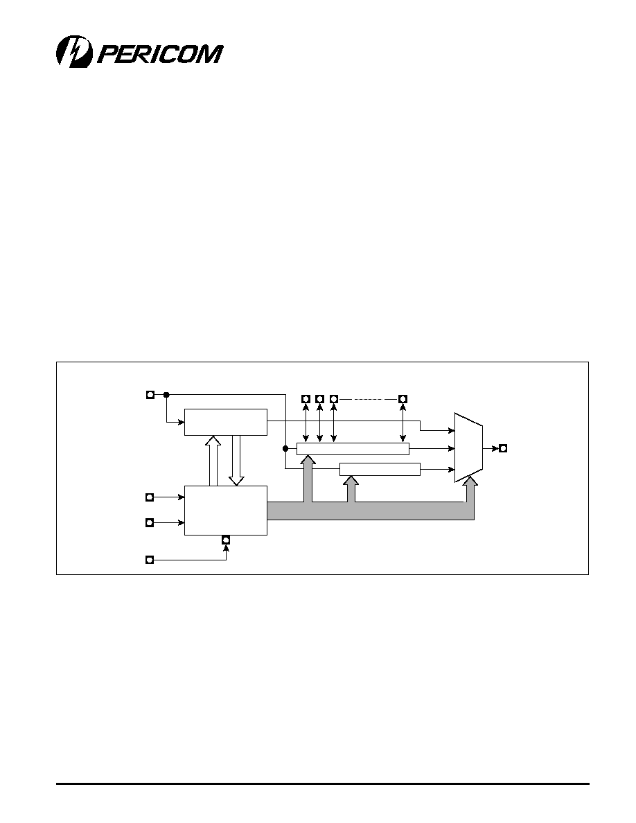
72
09/18/00 Rev 1.1
12345678901234567890123456789012123456789012345678901234567890121234567890123456789012345678901212345678901234567890123456789012123456
12345678901234567890123456789012123456789012345678901234567890121234567890123456789012345678901212345678901234567890123456789012123456
PI7C7100
3-Port PCI Bridge
ADVANCE INFORMATION
15. IEEE 1149.1 Compatible JTAG Controller
An IEEE 1149.1 compatible Test Access Port (TAP) controller and associated TAP pins are provided to support boundary
scan in PI7C7100 for board-level continuity test and diagnostics. The TAP pins assigned are TCK, TDI, TDO, TMS and
TRST#. All digital input, output, input/output pins are tested except TAP pins and clock pin.
The IEEE 1149.1 Test Logic consists of a TAP controller, an instruction register, and a group of test data registers including
Bypass, Device Identification and Boundary Scan registers. The TAP controller is a synchronous 16 state machine driven
by the Test Clock (TCK) and the Test Mode Select (TMS) pins. An independent power on reset circuit is provided to ensure
the machine is in TEST_LOGIC_RESET state at power-up. The JTAG signal lines are not active when the PCI resource
is operating PCI bus cycles.
PI7C7100 implements 3 basic instructions: BYPASS, SAMPLE/PRELOAD, EXTEST.
15.1 Boundary Scan Architecture
Boundary-scan test logic consists of a boundary-scan register and support logic. These are accessed through a Test
Access Port (TAP). The TAP provides a simple serial interface that allows all processor signal pins to be driven and/or
sampled, thereby providing direct control and monitoring of processor pins at the system level.
This mode of operation is valuable for design debugging and fault diagnosis since it permits examination of connections
not normally accessible to the test system. The following subsections describe the boundary-scan test logic elements:
TAP pins, instruction register, test data registers and TAP controller. Figure 15-1 illustrates how these pieces fit together
to form the JTAG unit.
15.1.1 TAP Pins
The PI7C7100's TAP pins form a serial port composed of four input connections (TMS, TCK, TRST# and TDI) and one output
connection (TDO). These pins are described in Table 15-1. The TAP pins provide access to the instruction register and
the test data registers.
15.1.2 Instruction Register
The Instruction Register (IR) holds instruction codes. These codes are shifted in through the Test Data Input (TDI) pin. The
instruction codes are used to select the specific test operation to be performed and the test data register to be accessed.
The instruction register is a parallel-loadable, master/slave-configured 2-bit wide, serial-shift register with latched outputs.
Data is shifted into and out of the IR serially through the TDI pin clocked by the rising edge of TCK. The shifted-in instruction
becomes active upon latching from the master stage to the slave stage. At that time the IR outputs along with the TAP
finite state machine outputs are decoded to select and control the test data register selected by that instruction. Upon
latching, all actions caused by any previous instructions terminate.
Boundary-Scan Register
Control and Clock Signals
TAP
Controller
Instruction
Register
Bypass Register
TDO
TDI
TMS
TCK
TRST#
TAP Pins
PI7C7100 System Pins
Figure 15-1. Test Access Port Block Diagram

73
09/18/00 Rev 1.1
123456789012345678901234567890121234567890123456789012345678901212345678901234567890123456789012123456789012345678901234567890121234567
123456789012345678901234567890121234567890123456789012345678901212345678901234567890123456789012123456789012345678901234567890121234567
PI7C7100
3-Port PCI Bridge
ADVANCE INFORMATION
The instruction determines the test to be performed, the test data register to be accessed, or both. The IR is two bits wide.
When the IR is selected, the most significant bit is connected to TDI, and the least significant bit is connected to TDO.
The value presented on the TDI pin is shifted into the IR on each rising edge of TCK. The TAP controller captures fixed
parallel data (01 binary ). When a new instruction is shifted in through TDI, the value 01 (binary) is always shifted out through
TDO, least significant bit first. This helps identify instructions in a long chain of serial data from several devices.
Upon activation of the TRST# reset pin, the latched instruction asynchronously changes to the idcode instruction. When
the TAP controller moves into the test state other than by reset activation, the opcode changes as TDI shifts, and becomes
active on the falling edge of TCK.
15.2 Boundary-Scan Instruction Set
The PI7C7100 supports three mandatory boundary-scan instructions (bypass, sample/preload and extest). The table
shown below lists the PI7C7100's boundary-scan instruction codes. The "reserved" code should not be used.
e
d
o
C
n
o
i
t
c
u
r
t
s
n
I
)
y
r
a
n
i
b
(
e
m
a
N
n
o
i
t
c
u
r
t
s
n
I
e
d
o
C
n
o
i
t
c
u
r
t
s
n
I
)
y
r
a
n
i
b
(
e
m
a
N
n
o
i
t
c
u
r
t
s
n
I
0
0
t
s
e
t
x
e
0
1
d
e
v
r
e
s
e
r
1
0
d
a
o
l
e
r
p
/
e
l
p
m
a
s
1
1
s
s
a
p
y
b
/
n
o
i
t
c
u
r
t
s
n
I
e
t
i
s
i
u
q
e
R
e
d
o
c
p
O
)
y
r
a
n
i
b
(
n
o
i
t
p
i
r
c
s
e
D
t
s
e
t
x
e
1
.
9
4
1
1
E
E
E
I
d
e
r
i
u
q
e
R
0
0
f
f
o
d
n
a
s
t
c
e
n
n
o
c
r
e
t
n
i
l
e
v
e
l
-
d
r
a
o
b
y
ll
a
c
i
p
y
t
,
y
r
t
i
u
c
r
i
c
l
a
n
r
e
t
x
e
f
o
g
n
i
t
s
e
t
s
e
t
a
i
t
i
n
i
t
s
e
t
x
E
.
O
D
T
d
n
a
I
D
T
n
e
e
w
t
e
b
r
e
t
s
i
g
e
r
n
a
c
s
-
y
r
a
d
n
u
o
b
e
h
t
s
t
c
e
n
n
o
c
t
s
e
t
x
e
.
y
r
t
i
u
c
r
i
c
p
i
h
c
o
t
n
i
d
e
t
f
i
h
s
s
e
u
l
a
v
y
b
n
e
v
i
r
d
e
r
a
s
e
u
l
a
v
n
i
p
l
a
n
g
i
s
t
u
p
t
u
o
ll
a
,
d
e
t
c
e
l
e
s
s
i
t
s
e
t
x
E
n
e
h
W
,
o
s
l
A
.
K
C
T
f
o
e
g
d
e
g
n
il
l
a
f
e
h
t
n
o
y
l
n
o
e
g
n
a
h
c
y
a
m
d
n
a
r
e
t
s
i
g
e
r
n
a
c
s
-
y
r
a
d
n
u
o
b
e
h
t
e
h
t
o
t
n
i
d
e
d
a
o
l
e
b
t
s
u
m
s
e
t
a
t
s
n
i
p
t
u
p
n
i
m
e
t
s
y
s
ll
a
,
d
e
t
c
e
l
e
s
s
i
t
s
e
t
x
e
n
e
h
w
.
K
C
T
f
o
e
g
d
e
-
g
n
i
s
i
r
e
h
t
n
o
r
e
t
s
i
g
e
r
n
a
c
s
-
y
r
a
d
n
u
o
b
/
e
l
p
m
a
s
d
a
o
l
e
r
p
1
.
9
4
1
1
E
E
E
I
d
e
r
i
u
q
e
R
1
0
:
s
n
o
i
t
c
n
u
f
o
w
t
s
m
r
o
f
r
e
p
d
a
o
l
e
r
p
/
e
l
p
m
a
S
t
u
o
h
t
i
w
K
C
T
f
o
e
g
d
e
g
n
i
s
i
r
e
h
t
n
o
d
e
r
u
t
p
a
c
s
i
n
o
i
t
c
u
r
t
s
n
i
e
l
p
m
a
s
e
h
t
f
o
t
o
h
s
p
a
n
s
A
r
e
t
s
i
g
e
r
n
a
c
s
-
y
r
a
d
n
u
o
b
s
e
s
u
a
c
n
o
i
t
c
u
r
t
s
n
i
e
h
T
.
n
o
i
t
a
r
e
p
o
l
a
m
r
o
n
h
t
i
w
g
n
i
r
e
f
r
e
t
n
i
.
n
e
v
i
r
d
g
n
i
e
b
e
u
l
a
v
e
h
t
e
l
p
m
a
s
o
t
s
t
u
p
t
u
o
h
t
i
w
d
e
t
a
i
c
o
s
s
a
s
ll
e
c
d
e
r
r
e
f
s
n
a
r
t
s
i
s
ll
e
c
n
a
c
s
-
y
r
a
d
n
u
o
b
e
h
t
n
i
d
l
e
h
a
t
a
d
e
h
t
K
C
T
f
o
e
g
d
e
g
n
il
l
a
f
e
h
t
n
O
·
m
e
t
s
y
s
e
h
t
o
t
d
e
il
p
p
a
s
i
a
t
a
d
d
e
h
c
t
a
l
e
v
a
l
s
e
h
t
y
ll
a
c
i
p
y
T
.
s
ll
e
c
r
e
t
s
i
g
e
r
e
v
a
l
s
e
h
t
o
t
.
n
o
i
t
c
u
r
t
s
n
i
t
s
e
t
x
e
e
h
t
a
i
v
s
t
u
p
t
u
o
e
d
o
c
d
i
1
.
9
4
1
1
E
E
E
I
l
a
n
o
i
t
p
O
0
1
d
e
v
r
e
s
e
R
s
s
a
p
y
b
1
.
9
4
1
1
E
E
E
I
d
e
r
i
u
q
e
R
1
1
0
.
s
n
i
p
O
D
T
d
n
a
I
D
T
n
e
e
w
t
e
b
r
e
t
s
i
g
e
r
s
s
a
p
y
b
t
i
b
-
e
n
o
e
h
t
s
t
c
e
l
e
s
n
o
i
t
c
u
r
t
s
n
i
s
s
a
p
y
B
s
i
h
t
e
l
i
h
W
.
r
e
t
s
i
g
e
r
s
s
a
p
y
b
e
h
t
s
e
s
s
e
c
c
a
t
a
h
t
n
o
i
t
c
u
r
t
s
n
i
y
l
n
o
e
h
t
s
i
)
y
r
a
n
i
b
(
m
e
t
s
y
s
n
o
t
c
e
f
f
e
o
n
e
v
a
h
s
r
e
t
s
i
g
e
r
a
t
a
d
t
s
e
t
r
e
h
t
o
ll
a
,
t
c
e
f
f
e
n
i
s
i
n
o
i
t
c
u
r
t
s
n
i
r
i
e
h
t
m
r
o
f
r
e
p
y
t
il
a
n
o
i
t
c
n
u
f
m
e
t
s
y
s
d
n
a
t
s
e
t
h
t
o
b
h
t
i
w
s
r
e
t
s
i
g
e
r
a
t
a
d
t
s
e
T
.
n
o
i
t
a
r
e
p
o
.
d
e
t
c
e
l
e
s
s
i
n
o
i
t
c
u
r
t
s
n
i
s
i
h
t
n
e
h
w
s
n
o
i
t
c
n
u
f
m
e
t
s
y
s
Table 15-1. TAP Pins

74
09/18/00 Rev 1.1
12345678901234567890123456789012123456789012345678901234567890121234567890123456789012345678901212345678901234567890123456789012123456
12345678901234567890123456789012123456789012345678901234567890121234567890123456789012345678901212345678901234567890123456789012123456
PI7C7100
3-Port PCI Bridge
ADVANCE INFORMATION
15.3 TAP Test Data Registers
The PI7C7100 contains two test data registers (bypass and boundary-scan). Each test data register selected by the TAP
controller is connected serially between TDI and TDO. TDI is connected to the test data register's most significant bit.
TDO is connected to the least significant bit. Data is shifted one bit position within the register towards TDO on each rising
edge of TCK. While any register is selected, data is transferred from TDI to TDO without inversion. The following sections
describe each of the test data registers.
15.4 Bypass Register
The required bypass register, a one-bit shift register, provides the shortest path between TDI and TDO when a bypass
instruction is in effect. This allows rapid movement of test data to and from other components on the board. This path can
be selected when no test operation is being performed on the PI7C7100.
15.5 Boundary-Scan Register
The boundary-scan register contains a cell for each pin as well as control cells for I/O and the high-impedance pin.
Table 15-2 shows the bit order of the PI7C7100 boundary-scan register. All table cells that contain "Control" select the
direction of bidirectional pins or high-impedance output pins. When a "0" is loaded into the control cell, the associated
pin(s) are high-impedance or selected as input.
The boundary-scan register is a required set of serial-shiftable register cells, configured in master/slave stages and
connected between each of the PI7C7100's pins and on-chip system logic. The VDD, GND, PLL, AGND, AVDD and JTAG
pins are NOT in the boundary-scan chain.
The boundary-scan register cells are dedicated logic and do not have any system function. Data may be loaded into the
boundary-scan register master cells from the device input pins and output pin-drivers in parallel by the mandatory sample/
preload and extest instructions. Parallel loading takes place on the rising edge of TCK.
Data may be scanned into the boundary-scan register serially via the TDI serial input pin, clocked by the rising edge of
TCK. When the required data has been loaded into the master-cell stages, it can be driven into the system logic at input
pins or onto the output pins on the falling edge of TCK state. Data may also be shifted out of the boundary-scan register
by means of the TDO serial output pin at the falling edge of TCK.
15.6 TAP Controller
The TAP (Test Access Port) controller is a 4-state synchronous finite state machine that controls the sequence of test
logic operations. The TAP can be controlled via a bus master. The bus master can be either automatic test equipment
or a component (i.e., PLD) that interfaces to the TAP. The TAP controller changes state only in response to a rising edge
of TCK. The value of the test mode state (TMS) input signal at a rising edge of TCK controls the sequence of state changes.
The TAP controller is initialized after power-up by applying a low to the TRST# pin. In addition, the TAP controller can be
initialized by applying a high signal level on the TMS input for a minimum of five TCK periods.
For greater detail on the behavior of the TAP controller, test logic in each controller state and the state machine and public
instructions, refer to the IEEE 1149.1 Standard Test Access Port and Boundary-Scan Architecture document (available
from the IEEE).

75
09/18/00 Rev 1.1
123456789012345678901234567890121234567890123456789012345678901212345678901234567890123456789012123456789012345678901234567890121234567
123456789012345678901234567890121234567890123456789012345678901212345678901234567890123456789012123456789012345678901234567890121234567
PI7C7100
3-Port PCI Bridge
ADVANCE INFORMATION
r
e
d
r
O
s
e
m
a
N
n
i
P
e
p
y
T
1
]
1
3
-
0
2
[
D
A
_
2
S
e
l
b
a
n
e
l
o
rt
n
o
c
2
]
1
2
[
D
A
_
2
S
t
u
p
t
u
o
3
]
1
2
[
D
A
_
2
S
t
u
p
n
i
4
#
R
R
E
P
_
2
S
e
l
b
a
n
e
l
o
rt
n
o
c
5
#
R
R
E
P
_
2
S
t
u
p
t
u
o
6
#
R
R
E
P
_
2
S
t
u
p
n
i
7
]
9
1
-
8
[
D
A
_
2
S
e
l
b
a
n
e
l
o
rt
n
o
c
8
]
6
1
[
D
A
_
2
S
t
u
p
t
u
o
9
]
6
1
[
D
A
_
2
S
t
u
p
n
i
0
1
#
E
M
A
R
F
_
2
S
e
l
b
a
n
e
l
o
rt
n
o
c
1
1
#
E
M
A
R
F
_
2
S
t
u
p
t
u
o
2
1
#
E
M
A
R
F
_
2
S
t
u
p
n
i
3
1
#
Y
D
R
T
_
2
S
/
#
L
E
S
V
E
D
_
2
S
e
l
b
a
n
e
l
o
rt
n
o
c
4
1
#
L
E
S
V
E
D
_
2
S
t
u
p
t
u
o
5
1
#
L
E
S
V
E
D
_
2
S
t
u
p
n
i
6
1
]
9
1
[
D
A
_
2
S
t
u
p
t
u
o
7
1
]
9
1
[
D
A
_
2
S
t
u
p
n
i
8
1
]
7
1
[
D
A
_
2
S
t
u
p
t
u
o
9
1
]
7
1
[
D
A
_
2
S
t
u
p
n
i
0
2
]
8
1
[
D
A
_
2
S
t
u
p
t
u
o
1
2
]
8
1
[
D
A
_
2
S
t
u
p
n
i
2
2
]
0
2
[
D
A
_
2
S
t
u
p
t
u
o
3
2
]
0
2
[
D
A
_
2
S
t
u
p
n
i
4
2
]
2
2
[
D
A
_
2
S
t
u
p
t
u
o
5
2
]
2
2
[
D
A
_
2
S
t
u
p
n
i
6
2
]
4
2
[
D
A
_
2
S
t
u
p
t
u
o
7
2
]
4
2
[
D
A
_
2
S
t
u
p
n
i
8
2
]
3
2
[
D
A
_
2
S
t
u
p
t
u
o
9
2
]
3
2
[
D
A
_
2
S
t
u
p
n
i
0
3
]
3
-
0
[
E
B
C
_
2
S
e
l
b
a
n
e
l
o
rt
n
o
c
1
3
]
3
[
E
B
C
_
2
S
t
u
p
t
u
o
2
3
]
3
[
E
B
C
_
2
S
t
u
p
n
i
3
3
]
5
2
[
D
A
_
2
S
t
u
p
t
u
o
4
3
]
5
2
[
D
A
_
2
S
t
u
p
n
i
5
3
]
6
2
[
D
A
_
2
S
t
u
p
t
u
o
r
e
d
r
O
s
e
m
a
N
n
i
P
e
p
y
T
6
3
]
6
2
[
D
A
_
2
S
t
u
p
n
i
7
3
]
8
2
[
D
A
_
2
S
t
u
p
t
u
o
8
3
]
8
2
[
D
A
_
2
S
t
u
p
n
i
9
3
]
7
2
[
D
A
_
2
S
t
u
p
t
u
o
0
4
]
7
2
[
D
A
_
2
S
t
u
p
n
i
1
4
]
9
2
[
D
A
_
2
S
t
u
p
t
u
o
2
4
]
9
2
[
D
A
_
2
S
t
u
p
n
i
3
4
]
0
3
[
D
A
_
2
S
t
u
p
t
u
o
4
4
]
0
3
[
D
A
_
2
S
t
u
p
n
i
5
4
]
1
3
[
D
A
_
2
S
t
u
p
t
u
o
6
4
]
1
3
[
D
A
_
2
S
t
u
p
n
i
7
4
#
]
0
[
T
N
G
_
2
S
e
l
b
a
n
e
l
o
rt
n
o
c
8
4
#
]
0
[
T
N
G
_
2
S
t
u
p
t
u
o
9
4
#
]
0
[
Q
E
R
_
2
S
t
u
p
n
i
0
5
#
]
1
[
Q
E
R
_
2
S
t
u
p
n
i
1
5
#
]
1
[
T
N
G
_
2
S
t
u
p
t
u
o
2
5
#
]
2
[
T
N
G
_
2
S
t
u
p
t
u
o
3
5
#
]
2
[
Q
E
R
_
2
S
t
u
p
n
i
4
5
#
]
3
[
Q
E
R
_
2
S
t
u
p
n
i
5
5
#
]
3
[
T
N
G
_
2
S
t
u
p
t
u
o
6
5
#
]
4
[
T
N
G
_
2
S
t
u
p
t
u
o
7
5
#
]
4
[
Q
E
R
_
2
S
t
u
p
n
i
8
5
#
]
5
[
Q
E
R
_
2
S
t
u
p
n
i
9
5
#
]
5
[
T
N
G
_
2
S
t
u
p
t
u
o
0
6
#
]
6
[
T
N
G
_
2
S
t
u
p
t
u
o
1
6
#
]
6
[
Q
E
R
_
2
S
t
u
p
n
i
2
6
#
]
7
[
Q
E
R
_
2
S
t
u
p
n
i
3
6
#
]
7
[
T
N
G
_
2
S
t
u
p
t
u
o
4
6
#
T
E
S
E
R
_
2
S
t
u
p
t
u
o
5
6
#
N
F
C
_
S
t
u
p
n
i
6
6
#
N
E
_
1
S
t
u
p
n
i
7
6
#
N
E
_
2
S
t
u
p
n
i
8
6
#
M
T
_
N
A
C
S
t
u
p
n
i
9
6
N
E
_
N
A
C
S
t
u
p
n
i
0
7
M
T
_
L
L
P
t
u
p
n
i
r
e
d
r
O
s
e
m
a
N
n
i
P
e
p
y
T
1
7
S
S
A
P
Y
B
t
u
p
n
i
2
7
#
H
S
U
L
F
t
u
p
n
i
3
7
#
T
E
S
E
R
_
P
t
u
p
n
i
4
7
#
T
N
G
_
P
t
u
p
n
i
5
7
#
Q
E
R
_
P
e
l
b
a
n
e
l
o
rt
n
o
c
6
7
#
Q
E
R
_
P
t
u
p
t
u
o
7
7
]
1
3
-
0
2
[
D
A
_
P
e
l
b
a
n
e
l
o
rt
n
o
c
8
7
]
0
3
[
D
A
_
P
t
u
p
t
u
o
9
7
]
0
3
[
D
A
_
P
t
u
p
n
i
0
8
]
1
3
[
D
A
_
P
t
u
p
t
u
o
1
8
]
1
3
[
D
A
_
P
t
u
p
n
i
2
8
]
7
2
[
D
A
_
P
t
u
p
t
u
o
3
8
]
7
2
[
D
A
_
P
t
u
p
n
i
4
8
]
6
2
[
D
A
_
P
t
u
p
t
u
o
5
8
]
6
2
[
D
A
_
P
t
u
p
n
i
6
8
]
8
2
[
D
A
_
P
t
u
p
t
u
o
7
8
]
8
2
[
D
A
_
P
t
u
p
n
i
8
8
]
9
2
[
D
A
_
P
t
u
p
t
u
o
9
8
]
9
2
[
D
A
_
P
t
u
p
n
i
0
9
]
3
-
0
[
E
B
C
_
P
e
l
b
a
n
e
l
o
rt
n
o
c
1
9
]
3
[
E
B
C
_
P
t
u
p
t
u
o
2
9
]
3
[
E
B
C
_
P
t
u
p
n
i
3
9
]
4
2
[
D
A
_
P
t
u
p
t
u
o
4
9
]
4
2
[
D
A
_
P
t
u
p
n
i
5
9
]
5
2
[
D
A
_
P
t
u
p
t
u
o
6
9
]
5
2
[
D
A
_
P
t
u
p
n
i
7
9
]
3
2
[
D
A
_
P
t
u
p
t
u
o
8
9
]
3
2
[
D
A
_
P
t
u
p
n
i
9
9
]
2
2
[
D
A
_
P
t
u
p
t
u
o
0
0
1
]
2
2
[
D
A
_
P
t
u
p
n
i
1
0
1
L
E
S
D
I
_
P
t
u
p
n
i
2
0
1
]
1
2
[
D
A
_
P
t
u
p
t
u
o
3
0
1
]
1
2
[
D
A
_
P
t
u
p
n
i
4
0
1
]
0
2
[
D
A
_
P
t
u
p
t
u
o
5
0
1
]
0
2
[
D
A
_
P
t
u
p
n
i
Table 15-2. JTAG Boundary Register Order

76
09/18/00 Rev 1.1
12345678901234567890123456789012123456789012345678901234567890121234567890123456789012345678901212345678901234567890123456789012123456
12345678901234567890123456789012123456789012345678901234567890121234567890123456789012345678901212345678901234567890123456789012123456
PI7C7100
3-Port PCI Bridge
ADVANCE INFORMATION
r
e
d
r
O
s
e
m
a
N
n
i
P
e
p
y
T
6
0
1
]
9
1
-
8
[
D
A
_
P
e
l
b
a
n
e
l
o
rt
n
o
c
7
0
1
]
9
1
[
D
A
_
P
t
u
p
t
u
o
8
0
1
]
9
1
[
D
A
_
P
t
u
p
n
i
9
0
1
]
8
1
[
D
A
_
P
t
u
p
t
u
o
0
1
1
]
8
1
[
D
A
_
P
t
u
p
n
i
1
1
1
]
7
1
[
D
A
_
P
t
u
p
t
u
o
2
1
1
]
7
1
[
D
A
_
P
t
u
p
n
i
3
1
1
]
6
1
[
D
A
_
P
t
u
p
t
u
o
4
1
1
]
6
1
[
D
A
_
P
t
u
p
n
i
5
1
1
]
2
[
E
B
C
_
P
t
u
p
t
u
o
6
1
1
]
2
[
E
B
C
_
P
t
u
p
n
i
7
1
1
#
E
M
A
R
F
_
P
e
l
b
a
n
e
l
o
rt
n
o
c
8
1
1
#
E
M
A
R
F
_
P
t
u
p
t
u
o
9
1
1
#
E
M
A
R
F
_
P
t
u
p
n
i
0
2
1
#
Y
D
R
I
_
P
e
l
b
a
n
e
l
o
rt
n
o
c
1
2
1
#
Y
D
R
I
_
P
t
u
p
t
u
o
2
2
1
#
Y
D
R
I
_
P
t
u
p
n
i
3
2
1
#
Y
D
R
T
_
P
/
L
E
S
V
E
D
_
P
e
l
b
a
n
e
l
o
rt
n
o
c
4
2
1
#
Y
D
R
T
_
P
t
u
p
t
u
o
5
2
1
#
Y
D
R
T
_
P
t
u
p
n
i
6
2
1
#
L
E
S
V
E
D
_
P
t
u
p
t
u
o
7
2
1
#
L
E
S
V
E
D
_
P
t
u
p
n
i
8
2
1
#
P
O
T
S
_
P
e
l
b
a
n
e
l
o
rt
n
o
c
9
2
1
#
P
O
T
S
_
P
t
u
p
t
u
o
0
3
1
#
P
O
T
S
_
P
t
u
p
n
i
1
3
1
#
R
R
E
P
_
P
e
l
b
a
n
e
l
o
rt
n
o
c
2
3
1
#
R
R
E
P
_
P
t
u
p
t
u
o
3
3
1
#
R
R
E
P
_
P
t
u
p
n
i
4
3
1
#
K
C
O
L
_
P
e
l
b
a
n
e
l
o
rt
n
o
c
5
3
1
#
K
C
O
L
_
P
t
u
p
t
u
o
6
3
1
#
K
C
O
L
_
P
t
u
p
n
i
7
3
1
#
R
R
E
S
_
P
e
l
b
a
n
e
l
o
rt
n
o
c
8
3
1
#
R
R
E
S
_
P
t
u
p
t
u
o
9
3
1
]
3
1
[
D
A
_
P
t
u
p
t
u
o
0
4
1
]
3
1
[
D
A
_
P
t
u
p
n
i
r
e
d
r
O
s
e
m
a
N
n
i
P
e
p
y
T
1
4
1
]
4
1
[
D
A
_
P
t
u
p
t
u
o
2
4
1
]
4
1
[
D
A
_
P
t
u
p
n
i
3
4
1
]
1
1
[
D
A
_
P
t
u
p
t
u
o
4
4
1
]
1
1
[
D
A
_
P
t
u
p
n
i
5
4
1
]
5
1
[
D
A
_
P
t
u
p
t
u
o
6
4
1
]
5
1
[
D
A
_
P
t
u
p
n
i
7
4
1
]
2
1
[
D
A
_
P
t
u
p
t
u
o
8
4
1
]
2
1
[
D
A
_
P
t
u
p
n
i
9
4
1
]
8
[
D
A
_
P
t
u
p
t
u
o
0
5
1
]
8
[
D
A
_
P
t
u
p
n
i
1
5
1
]
1
[
E
B
C
_
P
t
u
p
t
u
o
2
5
1
]
1
[
E
B
C
_
P
t
u
p
n
i
3
5
1
]
9
[
D
A
_
P
t
u
p
t
u
o
4
5
1
]
9
[
D
A
_
P
t
u
p
n
i
5
5
1
]
7
-
0
[
D
A
_
P
e
l
b
a
n
e
l
o
rt
n
o
c
6
5
1
]
5
[
D
A
_
P
t
u
p
t
u
o
7
5
1
]
5
[
D
A
_
P
t
u
p
n
i
8
5
1
N
E
6
6
M
_
P
t
u
p
n
i
9
5
1
]
6
[
D
A
_
P
t
u
p
t
u
o
0
6
1
]
6
[
D
A
_
P
t
u
p
n
i
1
6
1
]
2
[
D
A
_
P
t
u
p
t
u
o
2
6
1
]
2
[
D
A
_
P
t
u
p
n
i
3
6
1
R
A
P
_
P
e
l
b
a
n
e
l
o
rt
n
o
c
4
6
1
R
A
P
_
P
t
u
p
t
u
o
5
6
1
R
A
P
_
P
t
u
p
n
i
6
6
1
]
0
[
D
A
_
P
t
u
p
t
u
o
7
6
1
]
0
[
D
A
_
P
t
u
p
n
i
8
6
1
]
0
[
E
B
C
_
P
t
u
p
t
u
o
9
6
1
]
0
[
E
B
C
_
P
t
u
p
n
i
0
7
1
]
7
[
D
A
_
P
t
u
p
t
u
o
1
7
1
]
7
[
D
A
_
P
t
u
p
n
i
2
7
1
]
0
1
[
D
A
_
P
t
u
p
t
u
o
3
7
1
]
0
1
[
D
A
_
P
t
u
p
n
i
4
7
1
]
1
[
D
A
_
P
t
u
p
t
u
o
5
7
1
]
1
[
D
A
_
P
t
u
p
n
i
r
e
d
r
O
s
e
m
a
N
n
i
P
e
p
y
T
6
7
1
]
3
[
D
A
_
P
t
u
p
t
u
o
7
7
1
]
3
[
D
A
_
P
t
u
p
n
i
8
7
1
]
4
[
D
A
_
P
t
u
p
t
u
o
9
7
1
]
4
[
D
A
_
P
t
u
p
n
i
0
8
1
]
7
-
0
[
D
A
_
1
S
e
l
b
a
n
e
l
o
rt
n
o
c
1
8
1
]
0
[
D
A
_
1
S
t
u
p
t
u
o
2
8
1
]
0
[
D
A
_
1
S
t
u
p
n
i
3
8
1
]
1
[
D
A
_
1
S
t
u
p
t
u
o
4
8
1
]
1
[
D
A
_
1
S
t
u
p
n
i
5
8
1
]
2
[
D
A
_
1
S
t
u
p
t
u
o
6
8
1
]
2
[
D
A
_
1
S
t
u
p
n
i
7
8
1
]
5
[
D
A
_
1
S
t
u
p
t
u
o
8
8
1
]
5
[
D
A
_
1
S
t
u
p
n
i
9
8
1
]
3
[
D
A
_
1
S
t
u
p
t
u
o
0
9
1
]
3
[
D
A
_
1
S
t
u
p
n
i
1
9
1
]
4
[
D
A
_
1
S
t
u
p
t
u
o
2
9
1
]
4
[
D
A
_
1
S
t
u
p
n
i
3
9
1
]
3
-
0
[
E
B
C
_
1
S
e
l
b
a
n
e
l
o
rt
n
o
c
4
9
1
]
0
[
E
B
C
_
1
S
t
u
p
t
u
o
5
9
1
]
0
[
E
B
C
_
1
S
t
u
p
n
i
6
9
1
]
7
[
D
A
_
1
S
t
u
p
t
u
o
7
9
1
]
7
[
D
A
_
1
S
t
u
p
n
i
8
9
1
]
6
[
D
A
_
1
S
t
u
p
t
u
o
9
9
1
]
6
[
D
A
_
1
S
t
u
p
n
i
0
0
2
]
9
1
-
8
[
D
A
_
1
S
e
l
b
a
n
e
l
o
rt
n
o
c
1
0
2
]
8
[
D
A
_
1
S
t
u
p
t
u
o
2
0
2
]
8
[
D
A
_
1
S
t
u
p
n
i
3
0
2
]
9
[
D
A
_
1
S
t
u
p
t
u
o
4
0
2
]
9
[
D
A
_
1
S
t
u
p
n
i
5
0
2
]
0
1
[
D
A
_
1
S
t
u
p
t
u
o
6
0
2
]
0
1
[
D
A
_
1
S
t
u
p
n
i
7
0
2
]
1
1
[
D
A
_
1
S
t
u
p
t
u
o
8
0
2
]
1
1
[
D
A
_
1
S
t
u
p
n
i
9
0
2
]
2
1
[
D
A
_
1
S
t
u
p
t
u
o
0
1
2
]
2
1
[
D
A
_
1
S
t
u
p
n
i
Table 15-2. JTAG Boundary Register Order
(continued)

77
09/18/00 Rev 1.1
123456789012345678901234567890121234567890123456789012345678901212345678901234567890123456789012123456789012345678901234567890121234567
123456789012345678901234567890121234567890123456789012345678901212345678901234567890123456789012123456789012345678901234567890121234567
PI7C7100
3-Port PCI Bridge
ADVANCE INFORMATION
r
e
d
r
O
s
e
m
a
N
n
i
P
e
p
y
T
1
1
2
]
4
1
[
D
A
_
1
S
t
u
p
t
u
o
2
1
2
]
4
1
[
D
A
_
1
S
t
u
p
n
i
3
1
2
]
3
1
[
D
A
_
1
S
t
u
p
t
u
o
4
1
2
]
3
1
[
D
A
_
1
S
t
u
p
n
i
5
1
2
]
5
1
[
D
A
_
1
S
t
u
p
t
u
o
6
1
2
]
5
1
[
D
A
_
1
S
t
u
p
n
i
7
1
2
#
R
R
E
S
_
1
S
t
u
p
n
i
8
1
2
R
A
P
_
1
S
e
l
b
a
n
e
l
o
rt
n
o
c
9
1
2
R
A
P
_
1
S
t
u
p
t
u
o
0
2
2
R
A
P
_
1
S
t
u
p
n
i
1
2
2
]
1
[
E
B
C
_
1
S
t
u
p
t
u
o
2
2
2
]
1
[
E
B
C
_
1
S
t
u
p
n
i
3
2
2
#
Y
D
R
T
_
1
S
/
#
L
E
S
V
E
D
_
1
S
e
l
b
a
n
e
l
o
rt
n
o
c
4
2
2
#
L
E
S
V
E
D
_
1
S
t
u
p
t
u
o
5
2
2
#
L
E
S
V
E
D
_
1
S
t
u
p
n
i
6
2
2
#
P
O
T
S
_
1
S
e
l
b
a
n
e
l
o
rt
n
o
c
7
2
2
#
P
O
T
S
_
1
S
t
u
p
t
u
o
8
2
2
#
P
O
T
S
_
1
S
t
u
p
n
i
9
2
2
#
K
C
O
L
_
1
S
e
l
b
a
n
e
l
o
rt
n
o
c
0
3
2
#
K
C
O
L
_
1
S
t
u
p
t
u
o
1
3
2
#
K
C
O
L
_
1
S
t
u
p
n
i
2
3
2
#
R
R
E
P
_
1
S
e
l
b
a
n
e
l
o
rt
n
o
c
3
3
2
#
R
R
E
P
_
1
S
t
u
p
t
u
o
4
3
2
#
R
R
E
P
_
1
S
t
u
p
n
i
5
3
2
#
E
M
A
R
F
_
1
S
e
l
b
a
n
e
l
o
rt
n
o
c
6
3
2
#
E
M
A
R
F
_
1
S
t
u
p
t
u
o
7
3
2
#
E
M
A
R
F
_
1
S
t
u
p
n
i
8
3
2
#
Y
D
R
I
_
1
S
e
l
b
a
n
e
l
o
rt
n
o
c
9
3
2
#
Y
D
R
I
_
1
S
t
u
p
t
u
o
0
4
2
#
Y
D
R
I
_
1
S
t
u
p
n
i
1
4
2
#
Y
D
R
T
_
1
S
t
u
p
t
u
o
2
4
2
#
Y
D
R
T
_
1
S
t
u
p
n
i
3
4
2
#
]
7
1
[
D
A
_
1
S
t
u
p
t
u
o
4
4
2
#
]
7
1
[
D
A
_
1
S
t
u
p
n
i
5
4
2
#
]
6
1
[
D
A
_
1
S
t
u
p
t
u
o
r
e
d
r
O
s
e
m
a
N
n
i
P
e
p
y
T
6
4
2
#
]
6
1
[
D
A
_
1
S
t
u
p
n
i
7
4
2
]
1
3
-
0
2
[
D
A
_
1
S
e
l
b
a
n
e
l
o
rt
n
o
c
8
4
2
]
0
2
[
D
A
_
1
S
t
u
p
t
u
o
9
4
2
]
0
2
[
D
A
_
1
S
t
u
p
n
i
0
5
2
]
2
[
E
B
C
_
1
S
t
u
p
t
u
o
1
5
2
]
2
[
E
B
C
_
1
S
t
u
p
n
i
2
5
2
]
9
1
[
D
A
_
1
S
t
u
p
t
u
o
3
5
2
]
9
1
[
D
A
_
1
S
t
u
p
n
i
4
5
2
]
3
[
E
B
C
_
1
S
t
u
p
t
u
o
5
5
2
]
3
[
E
B
C
_
1
S
t
u
p
n
i
6
5
2
]
3
2
[
D
A
_
1
S
t
u
p
t
u
o
7
5
2
]
3
2
[
D
A
_
1
S
t
u
p
n
i
8
5
2
]
6
2
[
D
A
_
1
S
t
u
p
t
u
o
9
5
2
]
6
2
[
D
A
_
1
S
t
u
p
n
i
0
6
2
]
2
2
[
D
A
_
1
S
t
u
p
t
u
o
1
6
2
]
2
2
[
D
A
_
1
S
t
u
p
n
i
2
6
2
]
5
2
[
D
A
_
1
S
t
u
p
t
u
o
3
6
2
]
5
2
[
D
A
_
1
S
t
u
p
n
i
4
6
2
]
9
2
[
D
A
_
1
S
t
u
p
t
u
o
5
6
2
]
9
2
[
D
A
_
1
S
t
u
p
n
i
6
6
2
]
1
2
[
D
A
_
1
S
t
u
p
t
u
o
7
6
2
]
1
2
[
D
A
_
1
S
t
u
p
n
i
8
6
2
]
8
2
[
D
A
_
1
S
t
u
p
t
u
o
9
6
2
]
8
2
[
D
A
_
1
S
t
u
p
n
i
0
7
2
]
0
3
[
D
A
_
1
S
t
u
p
t
u
o
1
7
2
]
0
3
[
D
A
_
1
S
t
u
p
n
i
2
7
2
]
1
3
[
D
A
_
1
S
t
u
p
t
u
o
3
7
2
]
1
3
[
D
A
_
1
S
t
u
p
n
i
4
7
2
]
7
2
[
D
A
_
1
S
t
u
p
t
u
o
5
7
2
]
7
2
[
D
A
_
1
S
t
u
p
n
i
6
7
2
]
4
2
[
D
A
_
1
S
t
u
p
t
u
o
7
7
2
]
4
2
[
D
A
_
1
S
t
u
p
n
i
8
7
2
]
8
1
[
D
A
_
1
S
t
u
p
t
u
o
9
7
2
]
8
1
[
D
A
_
1
S
t
u
p
n
i
0
8
2
#
]
0
[
T
N
G
_
1
S
e
l
b
a
n
e
l
o
rt
n
o
c
r
e
d
r
O
s
e
m
a
N
n
i
P
e
p
y
T
1
8
2
#
]
0
[
T
N
G
_
1
S
t
u
p
t
u
o
2
8
2
#
]
0
[
Q
E
R
_
1
S
t
u
p
n
i
3
8
2
#
]
1
[
Q
E
R
_
1
S
t
u
p
n
i
4
8
2
#
]
1
[
T
N
G
_
1
S
t
u
p
t
u
o
5
8
2
#
]
2
[
T
N
G
_
1
S
t
u
p
t
u
o
6
8
2
#
]
2
[
Q
E
R
_
1
S
t
u
p
n
i
7
8
2
#
]
3
[
Q
E
R
_
1
S
t
u
p
n
i
8
8
2
#
]
3
[
T
N
G
_
1
S
t
u
p
t
u
o
9
8
2
#
]
4
[
T
N
G
_
1
S
t
u
p
t
u
o
0
9
2
#
]
4
[
Q
E
R
_
1
S
t
u
p
n
i
1
9
2
#
]
5
[
Q
E
R
_
1
S
t
u
p
n
i
2
9
2
#
]
5
[
T
N
G
_
1
S
t
u
p
t
u
o
3
9
2
#
]
6
[
T
N
G
_
1
S
t
u
p
t
u
o
4
9
2
#
]
6
[
Q
E
R
_
1
S
t
u
p
n
i
5
9
2
#
]
7
[
Q
E
R
_
1
S
t
u
p
n
i
6
9
2
#
]
7
[
T
N
G
_
1
S
t
u
p
t
u
o
7
9
2
#
T
E
S
E
R
_
1
S
t
u
p
t
u
o
8
9
2
]
7
-
0
[
D
A
_
2
S
e
l
b
a
n
e
l
o
rt
n
o
c
9
9
2
]
0
[
D
A
_
2
S
t
u
p
t
u
o
0
0
3
]
0
[
D
A
_
2
S
t
u
p
n
i
1
0
3
]
1
[
D
A
_
2
S
t
u
p
t
u
o
2
0
3
]
1
[
D
A
_
2
S
t
u
p
n
i
3
0
3
]
2
[
D
A
_
2
S
t
u
p
t
u
o
4
0
3
]
2
[
D
A
_
2
S
t
u
p
n
i
5
0
3
]
3
[
D
A
_
2
S
t
u
p
t
u
o
6
0
3
]
3
[
D
A
_
2
S
t
u
p
n
i
7
0
3
]
4
[
D
A
_
2
S
t
u
p
t
u
o
8
0
3
]
4
[
D
A
_
2
S
t
u
p
n
i
9
0
3
]
5
[
D
A
_
2
S
t
u
p
t
u
o
0
1
3
]
5
[
D
A
_
2
S
t
u
p
n
i
1
1
3
]
6
[
D
A
_
2
S
t
u
p
t
u
o
2
1
3
]
6
[
D
A
_
2
S
t
u
p
n
i
3
1
3
]
7
[
D
A
_
2
S
t
u
p
t
u
o
4
1
3
]
7
[
D
A
_
2
S
t
u
p
n
i
5
1
3
]
0
[
E
B
C
_
2
S
t
u
p
t
u
o
Table 15-2. JTAG Boundary Register Order
(continued)

78
09/18/00 Rev 1.1
12345678901234567890123456789012123456789012345678901234567890121234567890123456789012345678901212345678901234567890123456789012123456
12345678901234567890123456789012123456789012345678901234567890121234567890123456789012345678901212345678901234567890123456789012123456
PI7C7100
3-Port PCI Bridge
ADVANCE INFORMATION
r
e
d
r
O
s
e
m
a
N
n
i
P
e
p
y
T
6
1
3
]
0
[
E
B
C
_
2
S
t
u
p
n
i
7
1
3
]
8
[
D
A
_
2
S
t
u
p
t
u
o
8
1
3
]
8
[
D
A
_
2
S
t
u
p
n
i
9
1
3
]
0
1
[
D
A
_
2
S
t
u
p
t
u
o
0
2
3
]
0
1
[
D
A
_
2
S
t
u
p
n
i
1
2
3
]
9
[
D
A
_
2
S
t
u
p
t
u
o
2
2
3
]
9
[
D
A
_
2
S
t
u
p
n
i
3
2
3
]
1
1
[
D
A
_
2
S
t
u
p
t
u
o
4
2
3
]
1
1
[
D
A
_
2
S
t
u
p
n
i
5
2
3
N
E
6
6
M
_
S
t
u
p
n
i
6
2
3
]
2
1
[
D
A
_
2
S
t
u
p
t
u
o
7
2
3
]
2
1
[
D
A
_
2
S
t
u
p
n
i
8
2
3
]
4
1
[
D
A
_
2
S
t
u
p
t
u
o
9
2
3
]
4
1
[
D
A
_
2
S
t
u
p
n
i
0
3
3
]
1
[
E
B
C
_
2
S
t
u
p
t
u
o
1
3
3
]
1
[
E
B
C
_
2
S
t
u
p
n
i
2
3
3
]
5
1
[
D
A
_
2
S
t
u
p
t
u
o
3
3
3
]
5
1
[
D
A
_
2
S
t
u
p
n
i
4
3
3
R
A
P
_
2
S
e
l
b
a
n
e
l
o
rt
n
o
c
r
e
d
r
O
s
e
m
a
N
n
i
P
e
p
y
T
5
3
3
R
A
P
_
2
S
t
u
p
t
u
o
6
3
3
R
A
P
_
2
S
t
u
p
n
i
7
3
3
#
R
R
E
S
_
2
S
t
u
p
n
i
8
3
3
#
K
C
O
L
_
2
S
e
l
b
a
n
e
l
o
rt
n
o
c
9
3
3
#
K
C
O
L
_
2
S
t
u
p
t
u
o
0
4
3
#
K
C
O
L
_
2
S
t
u
p
n
i
1
4
3
#
Y
D
R
T
_
2
S
t
u
p
t
u
o
2
4
3
#
Y
D
R
T
_
2
S
t
u
p
n
i
3
4
3
#
P
O
T
S
_
2
S
e
l
b
a
n
e
l
o
rt
n
o
c
4
4
3
#
P
O
T
S
_
2
S
t
u
p
t
u
o
5
4
3
#
P
O
T
S
_
2
S
t
u
p
n
i
6
4
3
#
Y
D
R
I
_
2
S
e
l
b
a
n
e
l
o
rt
n
o
c
7
4
3
#
Y
D
R
I
_
2
S
t
u
p
t
u
o
8
4
3
#
Y
D
R
I
_
2
S
t
u
p
n
i
9
4
3
]
2
[
E
B
C
_
2
S
t
u
p
t
u
o
0
5
3
]
2
[
E
B
C
_
2
S
t
u
p
n
i
1
5
3
]
3
1
[
D
A
_
2
S
t
u
p
t
u
o
2
5
3
]
3
1
[
D
A
_
2
S
t
u
p
n
i
Table 15-2. JTAG Boundary Register Order
(continued)

79
09/18/00 Rev 1.1
123456789012345678901234567890121234567890123456789012345678901212345678901234567890123456789012123456789012345678901234567890121234567
123456789012345678901234567890121234567890123456789012345678901212345678901234567890123456789012123456789012345678901234567890121234567
PI7C7100
3-Port PCI Bridge
ADVANCE INFORMATION
Note:
Stresses greater than those listed under MAXIMUM RATINGS may cause permanent damage to the device. This is a
stress rating only and functional operation of the device at these or any conditions above those indicated in the operational
sections of this specification is not implied. Exposure to absolute maximum rating conditions for extended periods of time
may affect reliability.
16. Electrical and Timing Specifications
16.1 Maximum Ratings
(Above which the useful life may be impaired. For user guidelines, not tested).
e
r
u
t
a
r
e
p
m
e
T
e
g
a
r
o
t
S
C
°
0
5
1
+
o
t
C
°
5
6
d
e
il
p
p
a
r
e
w
o
P
h
t
i
w
e
r
u
t
a
r
e
p
m
e
T
t
n
e
i
b
m
A
C
°
0
7
+
o
t
C
°
0
V
A
&
s
t
u
p
n
I
(
s
l
a
i
t
n
e
t
o
P
d
n
u
o
r
G
o
t
e
g
a
t
l
o
V
y
l
p
p
u
S
C
C
V
,
D
D
)
y
l
n
o
V
6
.
3
+
o
t
V
3
.
0
e
g
a
t
l
o
V
t
u
p
n
I
C
D
V
6
.
3
+
o
t
V
5
.
0
16.2 3.3V DC Specifications
l
o
b
m
y
S
r
e
t
e
m
a
r
a
P
n
o
i
t
i
d
n
o
C
.
n
i
M
.
x
a
M
s
t
i
n
U
s
e
t
o
N
V
,
D
D
V
A
C
C
e
g
a
t
l
o
V
y
l
p
p
u
S
3
6
.
3
V
V
h
i
e
g
a
t
l
o
V
H
G
I
H
t
u
p
n
I
V
5
.
0
D
D
V
D
D
5
.
0
+
3
V
li
e
g
a
t
l
o
V
W
O
L
t
u
p
n
I
5
.
0
-
3
.
0
V
D
D
V
h
i
e
g
a
t
l
o
V
H
G
I
H
t
u
p
n
I
S
O
M
C
V
7
.
0
D
D
V
D
D
5
.
0
+
1
V
li
e
g
a
t
l
o
V
W
O
L
t
u
p
n
I
S
O
M
C
5
.
0
3
.
0
V
D
D
V
u
p
i
e
g
a
t
l
o
V
p
u
-
ll
u
P
t
u
p
n
I
V
7
.
0
D
D
3
I
li
t
n
e
r
r
u
C
e
g
a
k
a
e
L
t
u
p
n
I
V
<
0
n
i
V
<
D
D
0
1
±
A
µ
V
h
o
e
g
a
t
l
o
V
H
G
I
H
t
u
p
t
u
O
I
t
u
o
A
µ
0
0
5
=
V
9
.
0
D
D
V
V
l
o
e
g
a
t
l
o
V
W
O
L
t
u
p
t
u
O
I
t
u
o
A
µ
0
0
5
1
=
1
.
0
V
D
D
V
h
o
e
g
a
t
l
o
V
H
G
I
H
t
u
p
t
u
O
S
O
M
C
I
t
u
o
A
µ
0
0
5
=
V
D
D
5
.
0
-
2
V
l
o
e
g
a
t
l
o
V
W
O
L
t
u
p
t
u
O
S
O
M
C
I
t
u
o
A
µ
0
0
5
1
=
5
.
0
C
n
i
e
c
n
a
t
i
c
a
p
a
C
n
i
P
t
u
p
n
I
0
1
F
p
3
C
k
l
c
e
c
n
a
t
i
c
a
p
a
C
n
i
P
K
L
C
5
2
1
C
L
E
S
D
I
e
c
n
a
t
i
c
a
p
a
C
n
i
P
L
E
S
D
I
8
L
n
i
p
e
c
n
a
t
c
u
d
n
I
n
i
P
0
2
H
n
Notes:
1. CMOS Input pins: S_CFN#, TCK, TMS, TDI, TRST#, SCAN_EN, SCAN_TM#
2. CMOS Output pin: TDO
3. PCI pins: P_AD[31:0], P_CBE[3:0], P_PAR, P_FRAME#, P_IRDY#, P_TRDY#, P_DEVSEL#, P_STOP#, P_LOCK#, PIDSEL#,
P_PERR#, P_SERR#, P_REQ#, P_GNT#, P_RESET#, S1_AD[31:0], S2_AD[31:0], S1_CBE[3:0], S2_CBE[3:0], S1_PAR,
S2_PAR, S1_FRAME#, S2_FRAME#, S1_IRDY#, S2_IRDY#, S1_TRDY#, S2_TRDY#, S1_DEVSEL#, S2_DEVSEL#,
S1_STOP#, S2_STOP#, S1_LOCK#, S2_LOCK#, S1_PERR#, S2_PERR#, S1_SERR#, S2_SERR#, S1_REQ[7:0]#,
S2_REQ[7:0]#, S1_GNT[7:0]#, S2_GNT[7:0], S1_RESET#, S2_RESET#, S1_EN, S2_EN, P_FLUSH#.
80
09/18/00 Rev 1.1
12345678901234567890123456789012123456789012345678901234567890121234567890123456789012345678901212345678901234567890123456789012123456
12345678901234567890123456789012123456789012345678901234567890121234567890123456789012345678901212345678901234567890123456789012123456
PI7C7100
3-Port PCI Bridge
ADVANCE INFORMATION
l
o
b
m
y
S
r
e
t
e
m
a
r
a
P
n
o
i
t
i
d
n
o
C
.
n
i
M
.
x
a
M
s
t
i
n
U
T
W
E
K
S
]
0
:
5
1
[
T
U
O
K
L
C
_
S
g
n
o
m
a
W
E
K
S
0
0
.
1
s
n
T
Y
A
L
E
D
]
0
:
5
1
[
T
U
O
K
L
C
_
S
d
n
a
K
L
C
P
n
e
e
w
t
e
b
Y
A
L
E
D
d
a
o
l
F
p
0
2
7
0
1
T
E
L
C
Y
C
e
m
i
t
e
l
c
y
c
]
0
:
5
1
[
T
U
O
K
L
C
_
S
,
K
L
C
P
0
3
T
H
G
I
H
e
m
i
t
H
G
I
H
]
0
:
5
1
[
T
U
O
K
L
C
_
S
,
K
L
C
P
1
1
T
W
O
L
e
m
i
t
W
O
L
]
0
:
5
1
[
T
U
O
K
L
C
_
S
,
K
L
C
P
1
1
16.4 Primary and Secondary Buses at 33 MHz Clock Timing
l
o
b
m
y
S
r
e
t
e
m
a
r
a
P
.
n
i
M
.
x
a
M
s
t
i
n
U
T
u
s
s
l
a
n
g
i
s
d
e
s
u
b
-
K
L
C
o
t
e
m
i
t
p
u
t
e
s
t
u
p
n
I
3
,
2
,
1
7
s
n
T
)
p
t
p
(
u
s
t
n
i
o
p
-
o
t
-
t
n
i
o
p
-
K
L
C
o
t
e
m
i
t
p
u
t
e
s
t
u
p
n
I
3
,
2
,
1
2
1
,
0
1
T
h
K
L
C
m
o
r
f
e
m
i
t
d
l
o
h
l
a
n
g
i
s
t
u
p
n
I
2
,
1
0
T
l
a
v
s
l
a
n
g
i
s
d
e
s
u
b
-
y
a
l
e
d
d
il
a
v
l
a
n
g
i
s
o
t
K
L
C
3
,
2
,
1
2
1
1
T
)
p
t
p
(
l
a
v
t
n
i
o
p
-
o
t
-
t
n
i
o
p
-
y
a
l
e
d
d
il
a
v
l
a
n
g
i
s
o
t
K
L
C
3
,
2
,
1
2
2
1
T
n
o
y
a
l
e
d
e
v
i
t
c
a
o
t
t
a
o
l
F
2
,
1
2
T
f
f
o
y
a
l
e
d
t
a
o
l
f
o
t
e
v
i
t
c
A
2
,
1
8
2
V
test
T
val
T
on
T
h
Valid
V
test
1.5V for 5V signals: 0.4 V
CC
for 3.3V signals
Valid
T
su
Input
Note:
Output
CLK
T
off
T
inval
Figure 16-1. PCI Signal Timing Measurement Conditions
16.5 Power Consumption
r
e
t
e
m
a
r
a
P
l
a
c
i
p
y
T
s
t
i
n
U
n
o
i
t
p
m
u
s
n
o
C
r
e
w
o
P
0
0
6
W
m
I
,
t
n
e
r
r
u
C
y
l
p
p
u
S
C
C
2
8
1
A
m
1. See Figure 16-1 PCI Signal Timing Measurement Conditions.
2. All primary interface signals are synchronized to P_CLK. All secondary interface signals are synchronized to S_CLKOUT.
3. Point-to-point signals are p_req#, s1_req#<7:0>, s2_req#<7:0>, p_gnt#, s1_gnt#<7:0>, and s2_gnt#<7:0>. Bused signals
are p_ad, p_cbe#, p_par, p_perr#, p_serr#, p_frame#, p_irdy#, p_trdy#, p_lock#, p_devsel#, p_stop#, p_idsel, s1_ad,
s1_cbe#, s1_par, s1_perr#, s1_serr#, s1_frame#, s1_irdy#, s1_trdy#, s1_lock#, s1_devsel#, s1_stop#, s2_ad, s2_cbe#,
s3_par, s2_perr#, s2_serr#, s2_frame#, s2_irdy#, s2_trdy#, s2_lock#, s2_devsel#, and s2_stop#.
16.3 3.3V AC Specifications
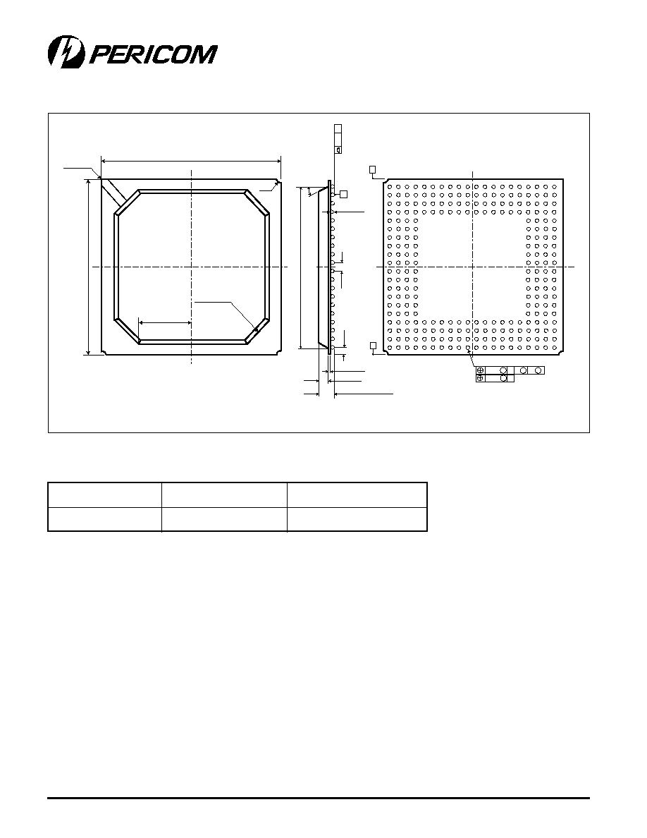
81
09/18/00 Rev 1.1
123456789012345678901234567890121234567890123456789012345678901212345678901234567890123456789012123456789012345678901234567890121234567
123456789012345678901234567890121234567890123456789012345678901212345678901234567890123456789012123456789012345678901234567890121234567
PI7C7100
3-Port PCI Bridge
ADVANCE INFORMATION
PIN #1
CORNER
20
0.15
19 18 17 16 15 14 13 12 11 10 9 8 7 6 5 4 3 2 1
A
B
C
D
E
F
G
H
J
K
L
M
N
P
R
T
U
V
W
Y
A
8.00
4 x 45° CHAMFER
2.33 Min. / 3.50Max.
27.00 ± 0.15
ø1.0
(3X)
0.60 ± 0.1
30
±
2°
SEA
TING
PLANE
1.27
1.44
BSC
24.00
±
0.1
256 x ø0.75 ± 0.15
0.56 ± 0.05
1.17 ± 0.1
0.30 S
0.10 S
S
S
C
C
B
B
C
C
A
27.00
±
0.15
(4X)
17. 256-Pin PBGA Package
TOP
BOTTOM
17.1 Part Number Ordering Information
t
r
a
P
e
g
a
k
c
a
P
-
n
i
P
e
r
u
t
a
r
e
p
m
e
T
A
N
C
0
0
1
7
C
7
I
P
A
G
B
P
-
6
5
2
C
°
0
7
+
o
t
C
°
0
Figure 17-1. 256-Pin PBGA Package

82
09/18/00 Rev 1.1
12345678901234567890123456789012123456789012345678901234567890121234567890123456789012345678901212345678901234567890123456789012123456
12345678901234567890123456789012123456789012345678901234567890121234567890123456789012345678901212345678901234567890123456789012123456
PI7C7100
3-Port PCI Bridge
ADVANCE INFORMATION

PI7C7100
3-Port
PCI Bridge
Appendix A
Timing
Diagrams

A-2
04/18/00
123456789012345678901234567890121234567890123456789012345678901212345678901234567890123456789012123456789012345678901234567890121234
123456789012345678901234567890121234567890123456789012345678901212345678901234567890123456789012123456789012345678901234567890121234
Appendix A
PI7C7100
3-Port PCI Bridge
ADVANCE INFORMATION
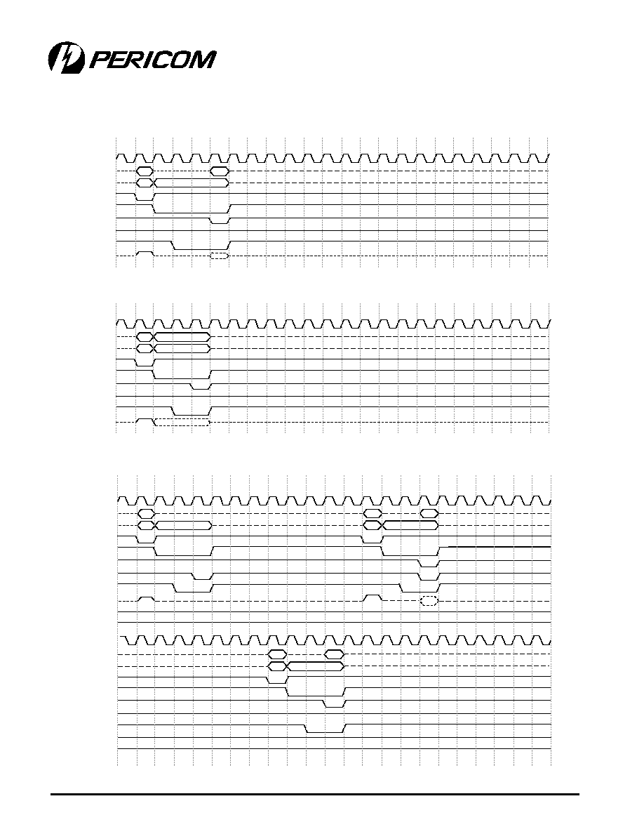
12345678901234567890123456789012123456789012345678901234567890121234567890123456789012345678901212345678901234567890123456789012123
12345678901234567890123456789012123456789012345678901234567890121234567890123456789012345678901212345678901234567890123456789012123
Appendix A
PI7C7100
3-Port PCI Bridge
A-3
04/18/00
ADVANCE INFORMATION
B
Addr
Data
Byte Enables
0
1
2
3
4
5
6
7
8
9
10
11
12
P_CLK
P_AD [31:0]
P_CBE [3:0]
P_FRAME_L
P_IRDY_L
P_TRDY_L
P_STOP_L
P_DEVSEL_L
P_IDSEL
13
14
15
16
17
18
19
20
21
22
Figure 2. Configuration Write Transaction
A
Addr
Data
Byte Enables
0
1
2
3
4
5
6
7
8
9
10
11
12
P_CLK
P_AD [31:0]
P_CBE [3:0]
P_FRAME_L
P_IRDY_L
P_TRDY_L
P_STOP_L
P_DEVSEL_L
P_IDSEL
13
14
15
16
17
18
19
20
21
22
Figure 1. Configuration Read Transaction
Addr
Data
Byte Enables
A
A
Addr
Byte Enables
Addr
Data
Byte Enables
A
0
1
2
3
4
5
6
7
8
9
10
11
12
13
14
15
16
17
18
19
20
21
22
0
1
2
3
4
5
6
7
8
9
10
11
12
13
14
15
16
17
18
19
20
21
22
P_CLK
P_AD [31:0]
P_CBE [3:0]
P_FRAME_L
P_IRDY_L
P_TRDY_L
P_STOP_L
P_DEVSEL_L
P_IDSEL
S_CLKOUT[0]
S_AD[31:0]
S_CBE[3:0]
S_FRAME_L
S_IRDY_L
S_TRDY_L
S_STOP_L
S_DEVSEL_L
S_GNT_L
S_REQ_L
P_GNT_L
P_REQ_L
Figure 3. Type 1 to Type 0 Configuration Read Transaction ( P --> S )
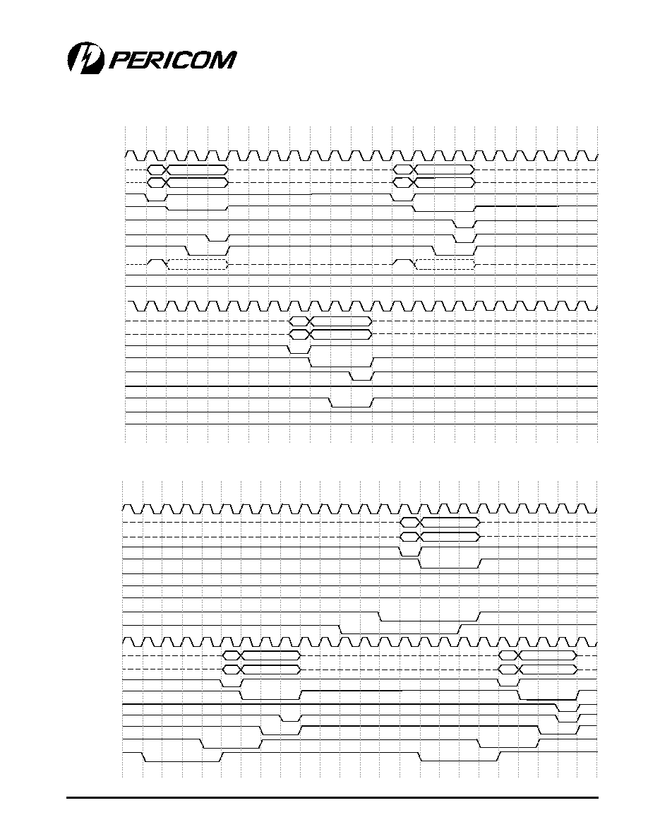
A-4
04/18/00
123456789012345678901234567890121234567890123456789012345678901212345678901234567890123456789012123456789012345678901234567890121234
123456789012345678901234567890121234567890123456789012345678901212345678901234567890123456789012123456789012345678901234567890121234
Appendix A
PI7C7100
3-Port PCI Bridge
ADVANCE INFORMATION
Addr
Data
Byte Enables
B
B
Addr
Data
Byte Enables
Addr
Data
Byte Enables
B
0
1
2
3
4
5
6
7
8
9
10
11
12
13
14
15
16
17
18
19
20
21
22
0
1
2
3
4
5
6
7
8
9
10
11
12
13
14
15
16
17
18
19
20
21
22
P_CLK
P_AD [31:0]
P_CBE [3:0]
P_FRAME_L
P_IRDY_L
P_TRDY_L
P_STOP_L
P_DEVSEL_L
P_IDSEL
S_CLKOUT[0]
S_AD[31:0]
S_CBE[3:0]
S_FRAME_L
S_IRDY_L
S_TRDY_L
S_STOP_L
S_DEVSEL_L
S_GNT_L
S_REQ_L
P_GNT_L
P_REQ_L
Figure 4. Type 1 to Type 0 Configuration Write Transaction ( P --> S )
Addr
Data
Addr
Data
Byte Enables
Byte Enables
B
1
B
Addr
Data
Byte Enables
Figure 5. Upstream Type 1 to Special Cycle Transaction
( S --> P )
0
1
2
3
4
5
6
7
8
9
10
11
12
13
14
15
16
17
18
19
20
21
22
0
1
2
3
4
5
6
7
8
9
10
11
12
13
14
15
16
17
18
19
20
21
22
P_CLK
P_AD [31:0]
P_CBE [3:0]
P_FRAME_L
P_IRDY_L
P_TRDY_L
P_STOP_L
P_DEVSEL_L
S_CLKOUT[0]
S_AD[31:0]
S_CBE[3:0]
S_FRAME_L
S_IRDY_L
S_TRDY_L
S_STOP_L
S_DEVSEL_L
S_GNT_L
S_REQ_L
P_GNT_L
P_REQ_L
23
23
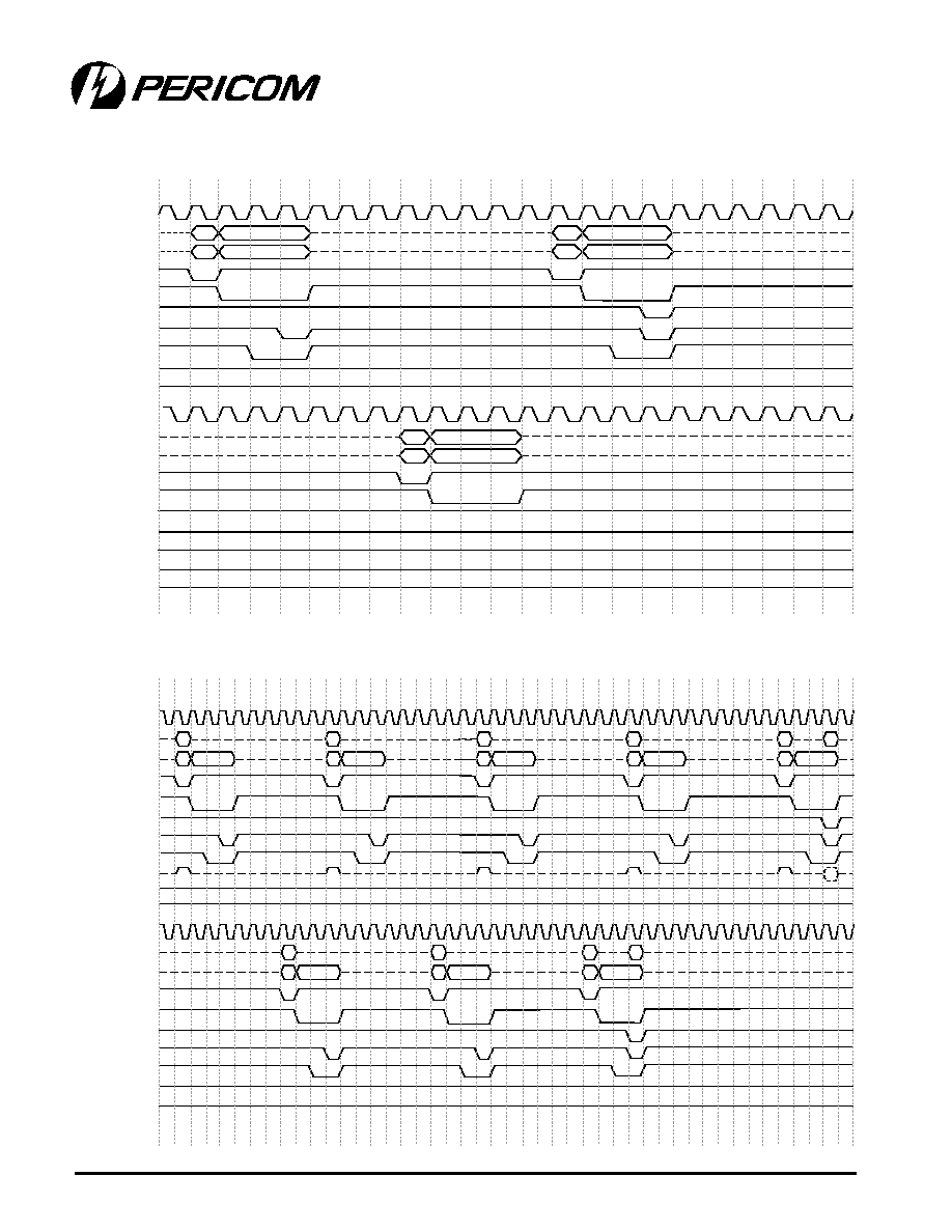
12345678901234567890123456789012123456789012345678901234567890121234567890123456789012345678901212345678901234567890123456789012123
12345678901234567890123456789012123456789012345678901234567890121234567890123456789012345678901212345678901234567890123456789012123
Appendix A
PI7C7100
3-Port PCI Bridge
A-5
04/18/00
ADVANCE INFORMATION
Addr
Data
Byte Enables
B
B
Addr
Data
Byte Enables
Addr
Data
Byte Enables
1
0
1
2
3
4
5
6
7
8
9
10
11
12
13
14
15
16
17
18
19
20
21
22
0
1
2
3
4
5
6
7
8
9
10
11
12
13
14
15
16
17
18
19
20
21
22
P_CLK
P_AD [31:0]
P_CBE [3:0]
P_FRAME_L
P_IRDY_L
P_TRDY_L
P_STOP_L
P_DEVSEL_L
S_CLKOUT[0]
S_AD[31:0]
S_CBE[3:0]
S_FRAME_L
S_IRDY_L
S_TRDY_L
S_STOP_L
S_DEVSEL_L
S_GNT_L
S_REQ_L
P_GNT_L
P_REQ_L
Figure 6. Downstream Type 1 to Special Cycle Transaction ( P --> S )
Addr
Addr
BytesEnables
B
B
Addr
Addr
Addr
Data
B
B
Byte Enables
Byte Enables
Byte Enables
Byte Enables
B
Addr
Addr
Addr
Data
B
B
B
Byte Enables
Byte Enables
Byte Enables
Figure 7. Downstream Type1 to Type1 Configuration Read Transaction ( P --> S )
0
2
4
6
8
10
12
14
16
18
20
22
24
26
28
30
32
34
36
38
40
42
44 45
1
3
5
7
9
11
13
15
17
19
21
23
25
27
29
31
33
35
37
39
41
43
0
2
4
6
8
10
12
14
16
18
20
22
24
26
28
30
32
34
36
38
40
42
44 45
1
3
5
7
9
11
13
15
17
19
21
23
25
27
29
31
33
35
37
39
41
43
P_CLK
P_AD [31:0]
P_CBE [3:0]
P_FRAME_L
P_IRDY_L
P_TRDY_L
P_STOP_L
P_DEVSEL_L
P_IDSEL
S_CLKOUT[0]
S_AD[31:0]
S_CBE[3:0]
S_FRAME_L
S_IRDY_L
S_TRDY_L
S_STOP_L
S_DEVSEL_L
S_GNT_L
S_REQ_L
P_GNT_L
P_REQ_L
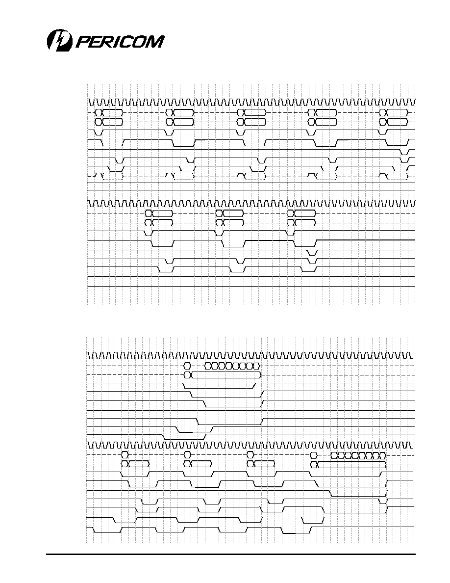
A-6
04/18/00
123456789012345678901234567890121234567890123456789012345678901212345678901234567890123456789012123456789012345678901234567890121234
123456789012345678901234567890121234567890123456789012345678901212345678901234567890123456789012123456789012345678901234567890121234
Appendix A
PI7C7100
3-Port PCI Bridge
ADVANCE INFORMATION
Addr
Addr
B
B
Addr
Addr
Addr
B
B
B
Addr
Addr
Addr
B
B
B
Byte Enables
Data
Byte Enables
Data
Byte Enables
Data
Byte Enables
Data
Byte Enables
Data
Byte Enables
Data
Byte Enables
Data
Byte Enables
Data
Figure 8. Downstream Type1 to Type1 Configuration Write Transaction ( P --> S )
0
2
4
6
8
10
12
14
16
18
20
22
24
26
28
30
32
34
36
38
40
42
44 45
1
3
5
7
9
11
13
15
17
19
21
23
25
27
29
31
33
35
37
39
41
43
0
2
4
6
8
10
12
14
16
18
20
22
24
26
28
30
32
34
36
38
40
42
44 45
1
3
5
7
9
11
13
15
17
19
21
23
25
27
29
31
33
35
37
39
41
43
P_CLK
P_AD [31:0]
P_CBE [3:0]
P_FRAME_L
P_IRDY_L
P_TRDY_L
P_STOP_L
P_DEVSEL_L
P_IDSEL
S_CLKOUT[0]
S_AD[31:0]
S_CBE[3:0]
S_FRAME_L
S_IRDY_L
S_TRDY_L
S_STOP_L
S_DEVSEL_L
S_GNT_L
S_REQ_L
P_GNT_L
P_REQ_L
6
Byte Enables
Addr
Data
Data
Data Data Data Data Data Data
Addr
Addr
Addr
6
6
6
Byte Enables
6
Addr
Data
Data
Data Data Data Data Data Data
Figure 9. Upstream Delayed Burst Memory Read Transaction ( S --> P )
0
2
4
6
8
10
12
14
16
18
20
22
24
26
28
30
32
34
36
38
40
42
44 45
1
3
5
7
9
11
13
15
17
19
21
23
25
27
29
31
33
35
37
39
41
43
46
0
2
4
6
8
10
12
14
16
18
20
22
24
26
28
30
32
34
36
38
40
42
44 45
1
3
5
7
9
11
13
15
17
19
21
23
25
27
29
31
33
35
37
39
41
43
P_CLK
P_AD [31:0]
P_CBE [3:0]
P_FRAME_L
P_IRDY_L
P_TRDY_L
P_STOP_L
P_DEVSEL_L
S_CLKOUT[0]
S_AD[31:0]
S_CBE[3:0]
S_FRAME_L
S_IRDY_L
S_TRDY_L
S_STOP_L
S_DEVSEL_L
S_GNT_L
S_REQ_L
P_GNT_L
P_REQ_L
46
ByteEnables
ByteEnables
ByteEnables
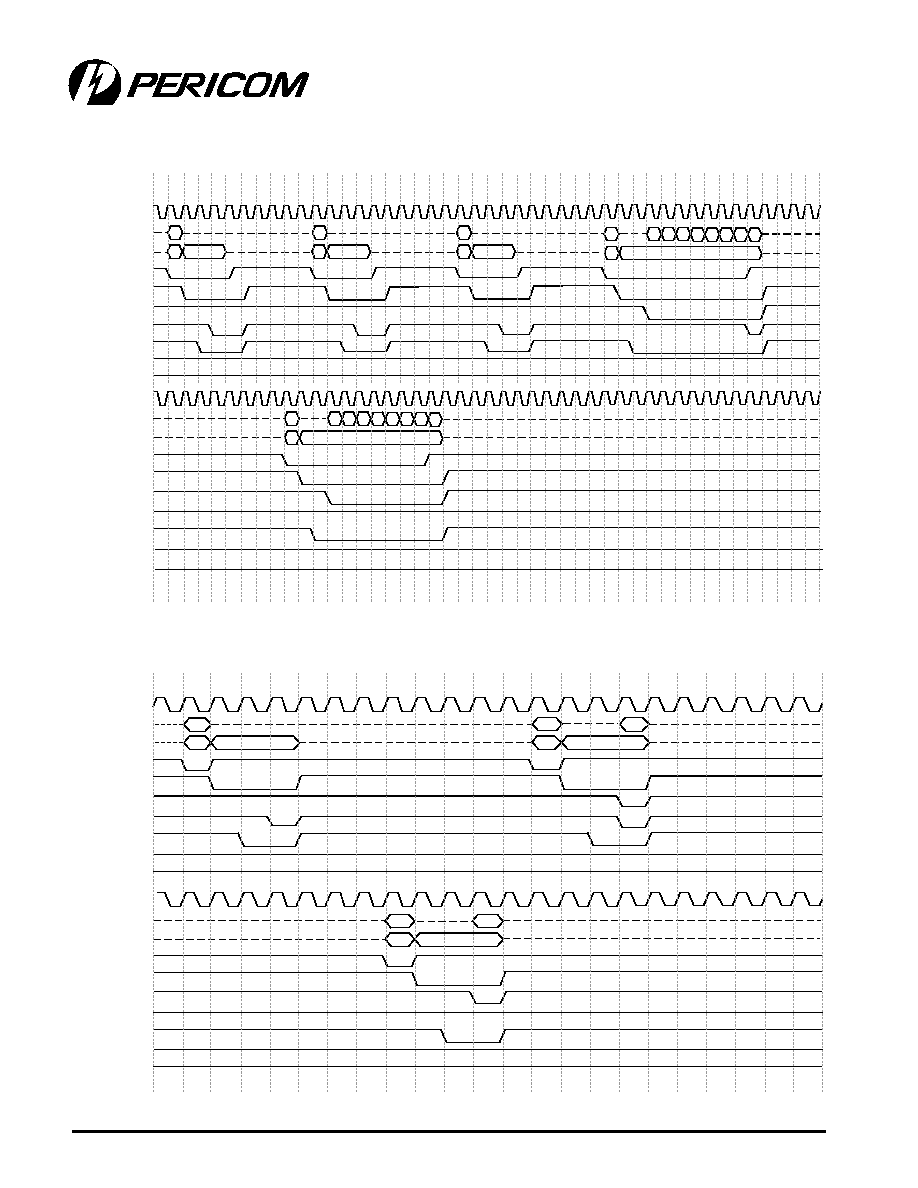
12345678901234567890123456789012123456789012345678901234567890121234567890123456789012345678901212345678901234567890123456789012123
12345678901234567890123456789012123456789012345678901234567890121234567890123456789012345678901212345678901234567890123456789012123
Appendix A
PI7C7100
3-Port PCI Bridge
A-7
04/18/00
ADVANCE INFORMATION
Addr
Addr
Addr
ByteEnables
ByteEnables
ByteEnables
6
6
6
Byte Enables
6
Addr
Data
Data
Data Data Data Data Data Data
6
Byte Enables
Addr
Data
Data
Data Data Data Data Data Data
Figure 10. Downstream Delayed Burst Memory Read Transaction ( P --> S )
0
2
4
6
8
10
12
14
16
18
20
22
24
26
28
30
32
34
36
38
40
42
44 45
1
3
5
7
9
11
13
15
17
19
21
23
25
27
29
31
33
35
37
39
41
43
0
2
4
6
8
10
12
14
16
18
20
22
24
26
28
30
32
34
36
38
40
42
44 45
1
3
5
7
9
11
13
15
17
19
21
23
25
27
29
31
33
35
37
39
41
43
P_CLK
P_AD [31:0]
P_CBE [3:0]
P_FRAME_L
P_IRDY_L
P_TRDY_L
P_STOP_L
P_DEVSEL_L
S_CLKOUT[0]
S_AD[31:0]
S_CBE[3:0]
S_FRAME_L
S_IRDY_L
S_TRDY_L
S_STOP_L
S_DEVSEL_L
S_GNT_L
S_REQ_L
P_GNT_L
P_REQ_L
Addr
Data
Byte Enables
6
6
Addr
Byte Enables
Addr
Data
Byte Enables
6
0
1
2
3
4
5
6
7
8
9
10
11
12
13
14
15
16
17
18
19
20
21
22
0
1
2
3
4
5
6
7
8
9
10
11
12
13
14
15
16
17
18
19
20
21
22
P_CLK
P_AD [31:0]
P_CBE [3:0]
P_FRAME_L
P_IRDY_L
P_TRDY_L
P_STOP_L
P_DEVSEL_L
S_CLKOUT[0]
S_AD[31:0]
S_CBE[3:0]
S_FRAME_L
S_IRDY_L
S_TRDY_L
S_STOP_L
S_DEVSEL_L
S_GNT_L
S_REQ_L
P_GNT_L
P_REQ_L
Figure 11. Downstream Delayed Memory Read Transaction (P/33MHz-->S/33MHz)
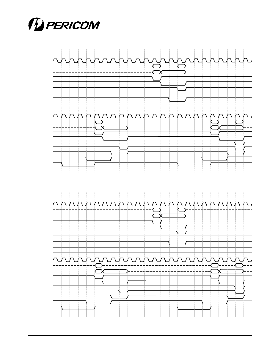
A-8
04/18/00
123456789012345678901234567890121234567890123456789012345678901212345678901234567890123456789012123456789012345678901234567890121234
123456789012345678901234567890121234567890123456789012345678901212345678901234567890123456789012123456789012345678901234567890121234
Appendix A
PI7C7100
3-Port PCI Bridge
ADVANCE INFORMATION
Addr
Data
Addr
Data
Byte Enables
Byte Enables
6
6
6
Addr
Byte Enables
Figure 12. Downstream Delayed Memory Read Transaction (S2/33MHz-->S1/33MHz)
0
1
2
3
4
5
6
7
8
9
10
11
12
13
14
15
16
17
18
19
20
21
22
0
1
2
3
4
5
6
7
8
9
10
11
12
13
14
15
16
17
18
19
20
21
22
S_CLKOUT[0]
S1_AD [31:0]
S1_CBE [3:0]
S1_FRAME_L
S1_IRDY_L
S1_TRDY_L
S1_STOP_L
S1_DEVSEL_L
S_CLKOUT[0]
S2_AD[31:0]
S2_CBE[3:0]
S2_FRAME_L
S2_IRDY_L
S2_TRDY_L
S2_STOP_L
S2_DEVSEL_L
S2_GNT_L
S2_REQ_L
S1_GNT_L
S1_REQ_L
23
23
Addr
Data
Addr
Data
Byte Enables
Byte Enables
6
6
6
Addr
Byte Enables
Figure 13. Downstream Delayed Memory Read Transaction (S1/33MHz-->S2/33MHz)
0
1
2
3
4
5
6
7
8
9
10
11
12
13
14
15
16
17
18
19
20
21
22
0
1
2
3
4
5
6
7
8
9
10
11
12
13
14
15
16
17
18
19
20
21
22
S_CLKOUT[0]
S2_AD [31:0]
S2_CBE [3:0]
S2_FRAME_L
S2_IRDY_L
S2_TRDY_L
S2_STOP_L
S2_DEVSEL_L
S_CLKOUT[0]
S1_AD[31:0]
S1_CBE[3:0]
S1_FRAME_L
S1_IRDY_L
S1_TRDY_L
S1_STOP_L
S1_DEVSEL_L
S1_GNT_L
S1_REQ_L
S2_GNT_L
S2_REQ_L
23
23
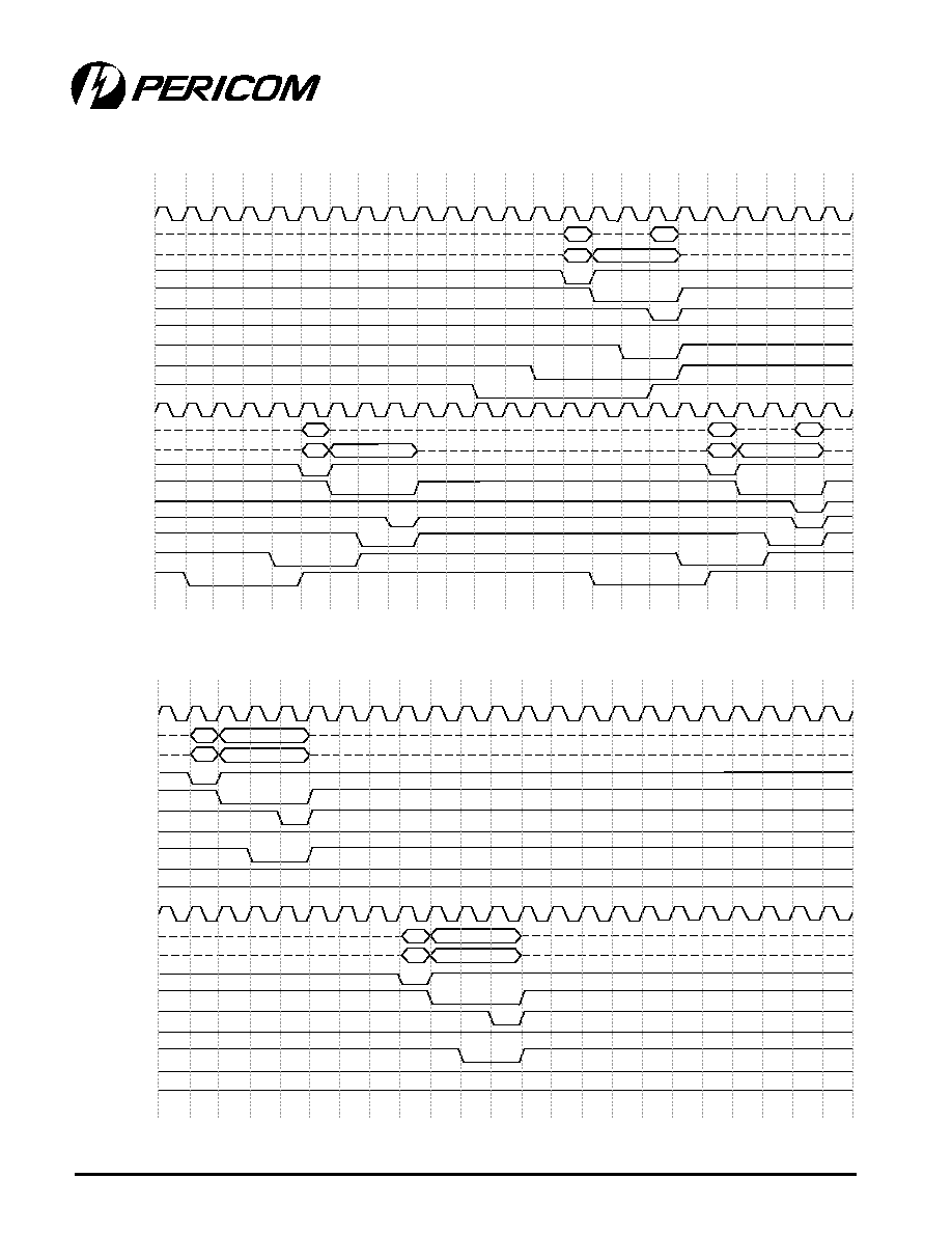
12345678901234567890123456789012123456789012345678901234567890121234567890123456789012345678901212345678901234567890123456789012123
12345678901234567890123456789012123456789012345678901234567890121234567890123456789012345678901212345678901234567890123456789012123
Appendix A
PI7C7100
3-Port PCI Bridge
A-9
04/18/00
ADVANCE INFORMATION
Addr
Data
Addr
Data
Byte Enables
Byte Enables
6
6
6
Addr
Byte Enables
Figure 14. Upstream Delayed Memory Read Transaction (S/33MHz-->P/33MHz)
0
1
2
3
4
5
6
7
8
9
10
11
12
13
14
15
16
17
18
19
20
21
22
0
1
2
3
4
5
6
7
8
9
10
11
12
13
14
15
16
17
18
19
20
21
22
P_CLK
P_AD [31:0]
P_CBE [3:0]
P_FRAME_L
P_IRDY_L
P_TRDY_L
P_STOP_L
P_DEVSEL_L
S_CLKOUT[0]
S_AD[31:0]
S_CBE[3:0]
S_FRAME_L
S_IRDY_L
S_TRDY_L
S_STOP_L
S_DEVSEL_L
S_GNT_L
S_REQ_L
P_GNT_L
P_REQ_L
23
Data
Byte Enables
7
Addr
Data
Byte Enables
7
Addr
Figure 15. Downstream Posted Memory Write Transaction (P/33MHz-->S/33MHz)
0
1
2
3
4
5
6
7
8
9
10
11
12
13
14
15
16
17
18
19
20
21
22
0
1
2
3
4
5
6
7
8
9
10
11
12
13
14
15
16
17
18
19
20
21
22
P_CLK
P_AD [31:0]
P_CBE [3:0]
P_FRAME_L
P_IRDY_L
P_TRDY_L
P_STOP_L
P_DEVSEL_L
S_CLKOUT[0]
S_AD[31:0]
S_CBE[3:0]
S_FRAME_L
S_IRDY_L
S_TRDY_L
S_STOP_L
S_DEVSEL_L
S_GNT_L
S_REQ_L
P_GNT_L
P_REQ_L
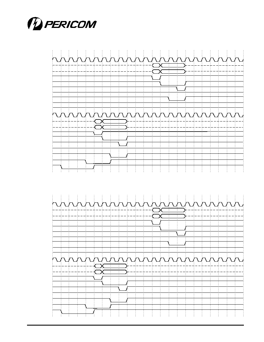
A-10
04/18/00
123456789012345678901234567890121234567890123456789012345678901212345678901234567890123456789012123456789012345678901234567890121234
123456789012345678901234567890121234567890123456789012345678901212345678901234567890123456789012123456789012345678901234567890121234
Appendix A
PI7C7100
3-Port PCI Bridge
ADVANCE INFORMATION
Addr
Data
Data
Byte Enables
Byte Enables
7
7
Addr
Figure 16. Downstream Posted Memory Write Transaction (S2/33MHz-->S1/33MHz)
0
1
2
3
4
5
6
7
8
9
10
11
12
13
14
15
16
17
18
19
20
21
22
0
1
2
3
4
5
6
7
8
9
10
11
12
13
14
15
16
17
18
19
20
21
22
S_CLKOUT[0]
S1_AD [31:0]
S1_CBE [3:0]
S1_FRAME_L
S1_IRDY_L
S1_TRDY_L
S1_STOP_L
S1_DEVSEL_L
S_CLKOUT[0]
S2_AD[31:0]
S2_CBE[3:0]
S2_FRAME_L
S2_IRDY_L
S2_TRDY_L
S2_STOP_L
S2_DEVSEL_L
S2_GNT_L
S2_REQ_L
S1_GNT_L
S1_REQ_L
Addr
Data
Data
Byte Enables
Byte Enables
7
7
Addr
Figure 17. Downstream Posted Memory Write Transaction (S1/33MHz-->S2/33MHz)
0
1
2
3
4
5
6
7
8
9
10
11
12
13
14
15
16
17
18
19
20
21
22
0
1
2
3
4
5
6
7
8
9
10
11
12
13
14
15
16
17
18
19
20
21
22
S_CLKOUT[0]
S2_AD [31:0]
S2_CBE [3:0]
S2_FRAME_L
S2_IRDY_L
S2_TRDY_L
S2_STOP_L
S2_DEVSEL_L
S_CLKOUT[0]
S1_AD[31:0]
S1_CBE[3:0]
S1_FRAME_L
S1_IRDY_L
S1_TRDY_L
S1_STOP_L
S1_DEVSEL_L
S1_GNT_L
S1_REQ_L
S2_GNT_L
S2_REQ_L
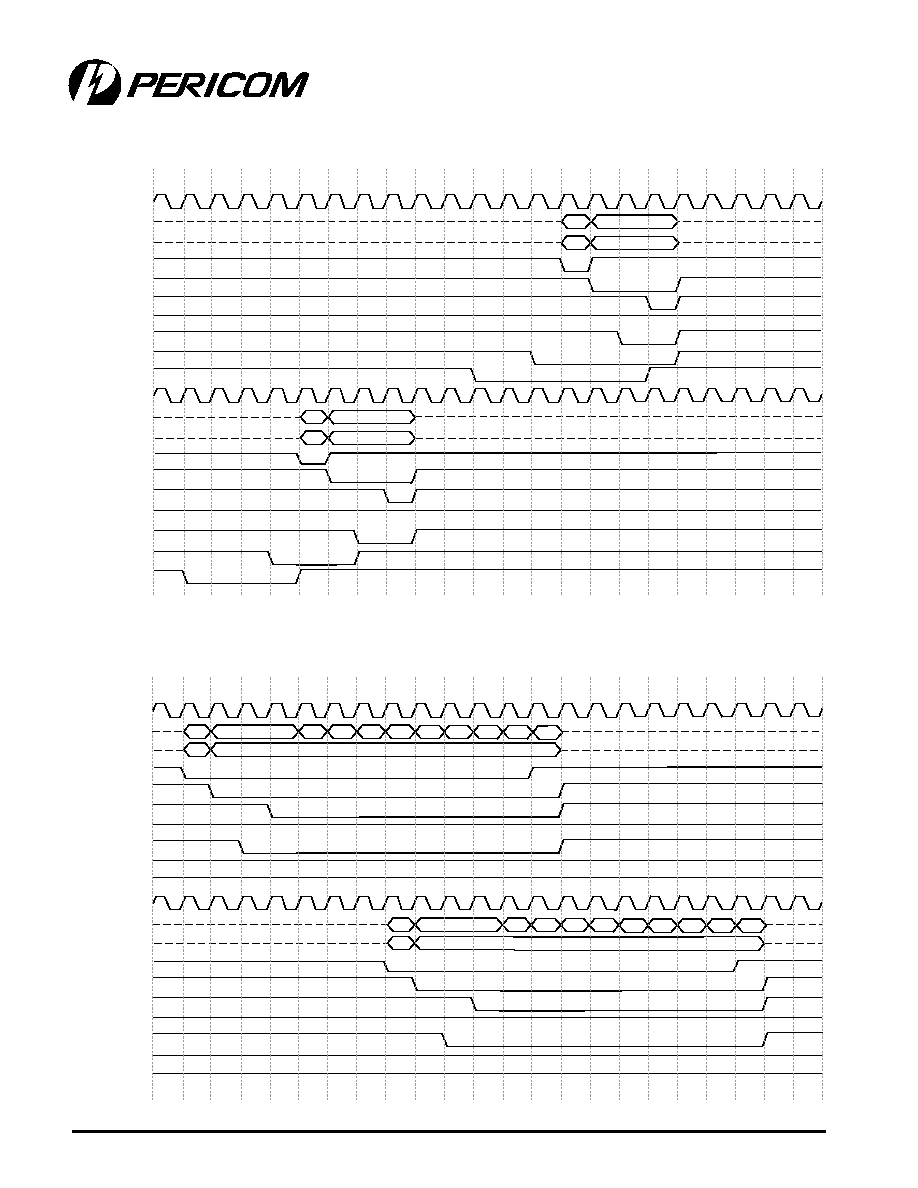
12345678901234567890123456789012123456789012345678901234567890121234567890123456789012345678901212345678901234567890123456789012123
12345678901234567890123456789012123456789012345678901234567890121234567890123456789012345678901212345678901234567890123456789012123
Appendix A
PI7C7100
3-Port PCI Bridge
A-11
04/18/00
ADVANCE INFORMATION
Addr
Data
Data
Byte Enables
Byte Enables
7
7
Addr
Figure 18. Upstream Posted Memory Write Transaction (S/33MHz-->P/33MHz)
0
1
2
3
4
5
6
7
8
9
10
11
12
13
14
15
16
17
18
19
20
21
22
0
1
2
3
4
5
6
7
8
9
10
11
12
13
14
15
16
17
18
19
20
21
22
P_CLK
P_AD [31:0]
P_CBE [3:0]
P_FRAME_L
P_IRDY_L
P_TRDY_L
P_STOP_L
P_DEVSEL_L
S_CLKOUT[0]
S_AD[31:0]
S_CBE[3:0]
S_FRAME_L
S_IRDY_L
S_TRDY_L
S_STOP_L
S_DEVSEL_L
S_GNT_L
S_REQ_L
P_GNT_L
P_REQ_L
Data
Data
Data Data Data Data Data Data Data Data
Byte Enables
7
Addr
Data
Data
Data Data Data Data Data Data Data Data
Byte Enables
7
Addr
Figure 19. Downstream Flow-Through Posted Memory Write Transaction (P/33MHz-->S/33MHz)
0
1
2
3
4
5
6
7
8
9
10
11
12
13
14
15
16
17
18
19
20
21
22
0
1
2
3
4
5
6
7
8
9
10
11
12
13
14
15
16
17
18
19
20
21
22
P_CLK
P_AD [31:0]
P_CBE [3:0]
P_FRAME_L
P_IRDY_L
P_TRDY_L
P_STOP_L
P_DEVSEL_L
S_CLKOUT[0]
S_AD[31:0]
S_CBE[3:0]
S_FRAME_L
S_IRDY_L
S_TRDY_L
S_STOP_L
S_DEVSEL_L
S_GNT_L
S_REQ_L
P_GNT_L
P_REQ_L
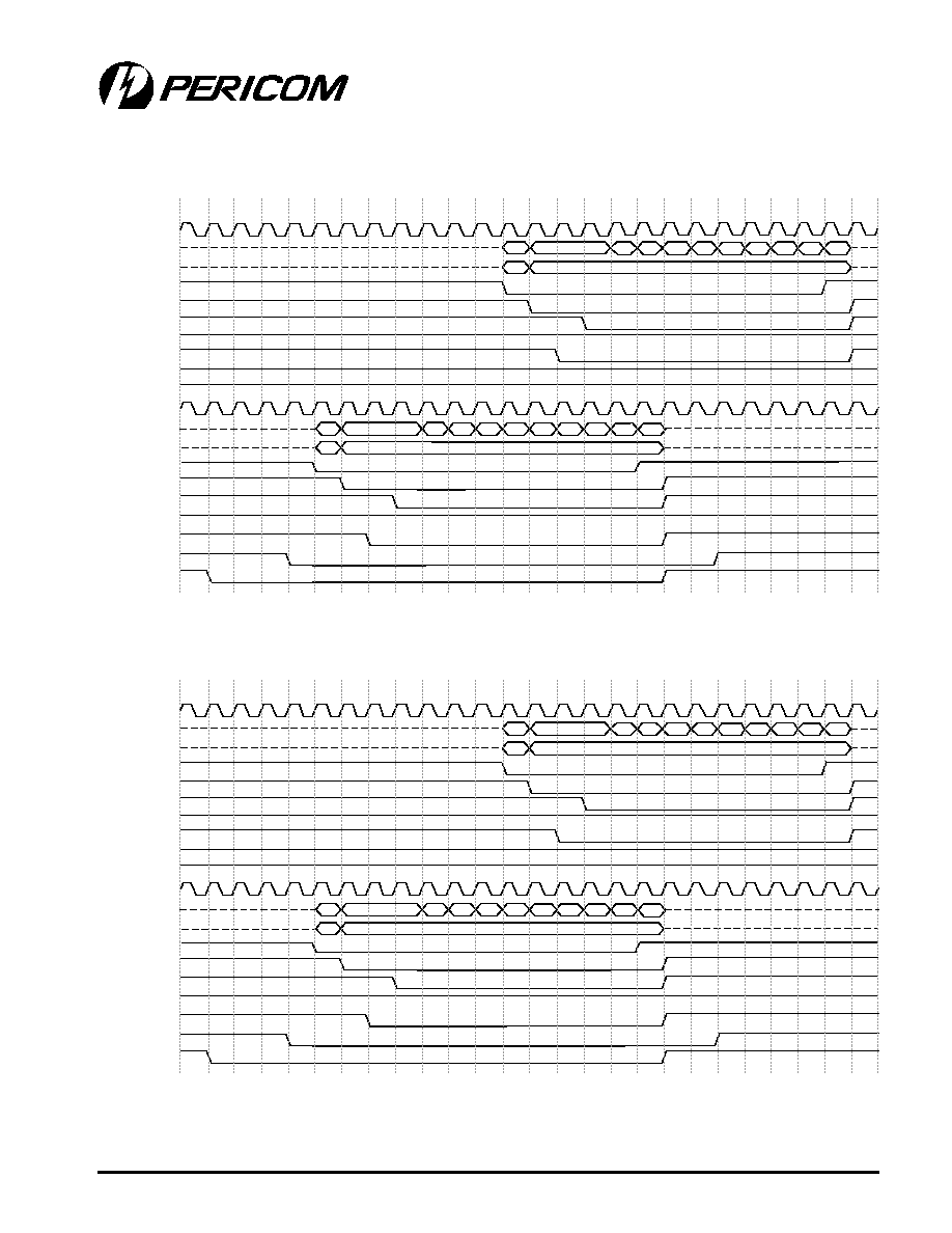
A-12
04/18/00
123456789012345678901234567890121234567890123456789012345678901212345678901234567890123456789012123456789012345678901234567890121234
123456789012345678901234567890121234567890123456789012345678901212345678901234567890123456789012123456789012345678901234567890121234
Appendix A
PI7C7100
3-Port PCI Bridge
ADVANCE INFORMATION
Addr
Data
Data Data Data Data Data Data Data Data Data
Data
Data
Data Data Data Data Data Data Data Data
Byte Enables
Byte Enables
7
7
Addr
Figure 20. Downstream Flow-Through Posted Memory Write Transaction (S2/33MHz-->S1/33MHz)
0
1
2
3
4
5
6
7
8
9
10
11
12
13 14
15
16
17
18
19
20
21
22
0
1
2
3
4
5
6
7
8
9
10
11
12
13 14
15
16
17
18
19
20
21
22
S_CLKOUT[0]
S1_AD [31:0]
S1_CBE [3:0]
S1_FRAME_L
S1_IRDY_L
S1_TRDY_L
S1_STOP_L
S1_DEVSEL_L
S_CLKOUT[0]
S2_AD[31:0]
S2_CBE[3:0]
S2_FRAME_L
S2_IRDY_L
S2_TRDY_L
S2_STOP_L
S2_DEVSEL_L
S2_GNT_L
S2_REQ_L
S1_GNT_L
S1_REQ_L
23
24
25
23
24
25
Addr
Data
Data Data Data Data Data Data Data Data Data
Data
Data
Data Data Data Data Data Data Data Data
Byte Enables
Byte Enables
7
7
Addr
Figure 21. Downstream Flow-Through Posted Memory Write Transaction (S1/33MHz-->S2/33MHz)
0
1
2
3
4
5
6
7
8
9
10
11
12
13 14
15
16
17
18
19
20
21
22
0
1
2
3
4
5
6
7
8
9
10
11
12
13 14
15
16
17
18
19
20
21
22
S_CLKOUT[0]
S2_AD [31:0]
S2_CBE [3:0]
S2_FRAME_L
S2_IRDY_L
S2_TRDY_L
S2_STOP_L
S2_DEVSEL_L
S_CLKOUT[0]
S1_AD[31:0]
S1_CBE[3:0]
S1_FRAME_L
S1_IRDY_L
S1_TRDY_L
S1_STOP_L
S1_DEVSEL_L
S1_GNT_L
S1_REQ_L
S2_GNT_L
S2_REQ_L
23
24
25
23
24
25
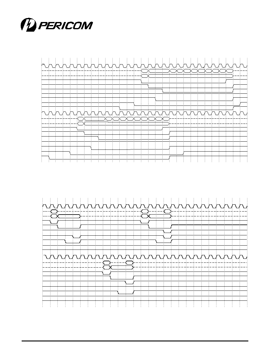
12345678901234567890123456789012123456789012345678901234567890121234567890123456789012345678901212345678901234567890123456789012123
12345678901234567890123456789012123456789012345678901234567890121234567890123456789012345678901212345678901234567890123456789012123
Appendix A
PI7C7100
3-Port PCI Bridge
A-13
04/18/00
ADVANCE INFORMATION
Addr
Data
Data Data Data Data Data Data Data Data Data
Data
Data
Data Data Data Data Data Data Data Data
Byte Enables
Byte Enables
7
7
Addr
Figure 22. Upstream Flow-Through Posted Memory Write Transaction (S/33MHz-->P/33MHz)
!
"
#
$
%
&
'
!
"
#
$
%
&
'
!
"
#
$
%
&
'
!
"
#
$
%
&
'
P_CLK
P_AD [31:0]
P_CBE [3:0]
P_FRAME_L
P_IRDY_L
P_TRDY_L
P_STOP_L
P_DEVSEL_L
S_CLKOUT[0]
S_AD[31:0]
S_CBE[3:0]
S_FRAME_L
S_IRDY_L
S_TRDY_L
S_STOP_L
S_DEVSEL_L
S_GNT_L
S_REQ_L
P_GNT_L
P_REQ_L
!
"
#
$
%
&
!
"
#
$
%
&
Addr
Data
Byte Enables
2
2
Addr
Byte Enables
Addr
Data
Byte Enables
2
0
1
2
3
4
5
6
7
8
9
10
11
12
13
14
15
16
17
18
19
20
21
22
0
1
2
3
4
5
6
7
8
9
10
11
12
13
14
15
16
17
18
19
20
21
22
23
24
25
26
P_CLK
P_AD [31:0]
P_CBE [3:0]
P_FRAME_L
P_IRDY_L
P_TRDY_L
P_STOP_L
P_DEVSEL_L
S_CLKOUT[0]
S_AD[31:0]
S_CBE[3:0]
S_FRAME_L
S_IRDY_L
S_TRDY_L
S_STOP_L
S_DEVSEL_L
S_GNT_L
S_REQ_L
P_GNT_L
P_REQ_L
23
24
25
26
Figure 23. Downstream Delayed I/O Read Transaction ( P --> S )
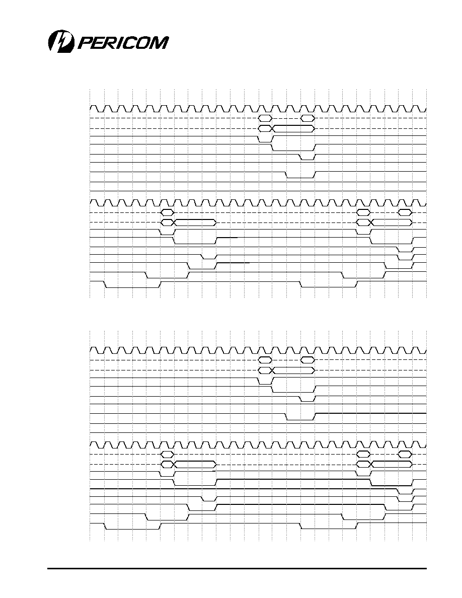
A-14
04/18/00
123456789012345678901234567890121234567890123456789012345678901212345678901234567890123456789012123456789012345678901234567890121234
123456789012345678901234567890121234567890123456789012345678901212345678901234567890123456789012123456789012345678901234567890121234
Appendix A
PI7C7100
3-Port PCI Bridge
ADVANCE INFORMATION
Addr
Data
Addr
Data
Byte Enables
Byte Enables
2
2
2
Addr
Byte Enables
Figure 24. Downstream Delayed I/O Read Transaction (S2/33MHz-->S1/33MHz)
0
1
2
3
4
5
6
7
8
9
10
11
12
13
14
15
16
17
18
19
20
21
22
0
1
2
3
4
5
6
7
8
9
10
11
12
13
14
15
16
17
18
19
20
21
22
S_CLKOUT[0]
S1_AD [31:0]
S1_CBE [3:0]
S1_FRAME_L
S1_IRDY_L
S1_TRDY_L
S1_STOP_L
S1_DEVSEL_L
S_CLKOUT[0]
S2_AD[31:0]
S2_CBE[3:0]
S2_FRAME_L
S2_IRDY_L
S2_TRDY_L
S2_STOP_L
S2_DEVSEL_L
S2_GNT_L
S2_REQ_L
S1_GNT_L
S1_REQ_L
23
23
Addr
Data
Addr
Data
Byte Enables
Byte Enables
2
2
2
Addr
Byte Enables
Figure 25. Downstream Delayed I/O Read Transaction (S1/33MHz-->S2/33MHz)
0
1
2
3
4
5
6
7
8
9
10
11
12
13
14
15
16
17
18
19
20
21
22
0
1
2
3
4
5
6
7
8
9
10
11
12
13
14
15
16
17
18
19
20
21
22
S_CLKOUT[0]
S2_AD [31:0]
S2_CBE [3:0]
S2_FRAME_L
S2_IRDY_L
S2_TRDY_L
S2_STOP_L
S2_DEVSEL_L
S_CLKOUT[0]
S1_AD[31:0]
S1_CBE[3:0]
S1_FRAME_L
S1_IRDY_L
S1_TRDY_L
S1_STOP_L
S1_DEVSEL_L
S1_GNT_L
S1_REQ_L
S2_GNT_L
S2_REQ_L
23
23
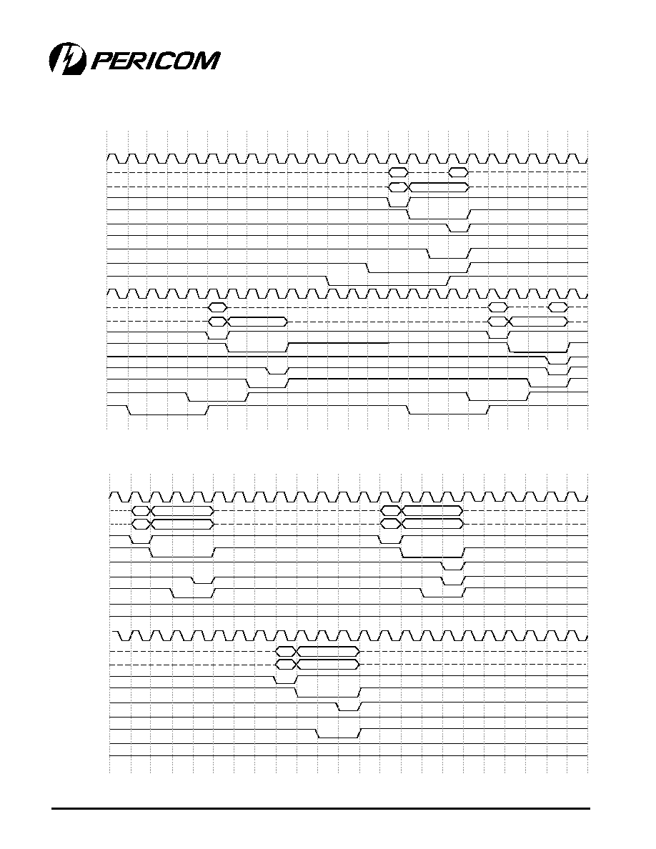
12345678901234567890123456789012123456789012345678901234567890121234567890123456789012345678901212345678901234567890123456789012123
12345678901234567890123456789012123456789012345678901234567890121234567890123456789012345678901212345678901234567890123456789012123
Appendix A
PI7C7100
3-Port PCI Bridge
A-15
04/18/00
ADVANCE INFORMATION
Addr
Data
Addr
Data
Byte Enables
Byte Enables
2
2
2
Addr
Byte Enables
Figure 26. Upstream Delayed I/O Read Transaction (S/33MHz-->P/33MHz)
0
1
2
3
4
5
6
7
8
9
10
11
12
13
14
15
16
17
18
19
20
21
22
0
1
2
3
4
5
6
7
8
9
10
11
12
13
14
15
16
17
18
19
20
21
22
P_CLK
P_AD [31:0]
P_CBE [3:0]
P_FRAME_L
P_IRDY_L
P_TRDY_L
P_STOP_L
P_DEVSEL_L
S_CLKOUT[0]
S_AD[31:0]
S_CBE[3:0]
S_FRAME_L
S_IRDY_L
S_TRDY_L
S_STOP_L
S_DEVSEL_L
S_GNT_L
S_REQ_L
P_GNT_L
P_REQ_L
23
Addr
Data
Byte Enables
3
3
Addr
Data
Byte Enables
Addr
Data
Byte Enables
3
0
1
2
3
4
5
6
7
8
9
10
11
12
13
14
15
16
17
18
19
20
21
22
0
1
2
3
4
5
6
7
8
9
10
11
12
13
14
15
16
17
18
19
20
21
22
P_CLK
P_AD [31:0]
P_CBE [3:0]
P_FRAME_L
P_IRDY_L
P_TRDY_L
P_STOP_L
P_DEVSEL_L
S_CLKOUT[0]
S_AD[31:0]
S_CBE[3:0]
S_FRAME_L
S_IRDY_L
S_TRDY_L
S_STOP_L
S_DEVSEL_L
S_GNT_L
S_REQ_L
P_GNT_L
P_REQ_L
Figure 27. Downstream Delayed I/O Write Transaction ( P --> S )
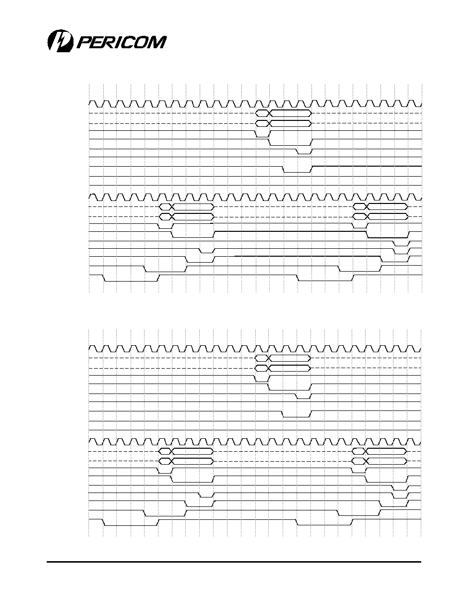
A-16
04/18/00
123456789012345678901234567890121234567890123456789012345678901212345678901234567890123456789012123456789012345678901234567890121234
123456789012345678901234567890121234567890123456789012345678901212345678901234567890123456789012123456789012345678901234567890121234
Appendix A
PI7C7100
3-Port PCI Bridge
ADVANCE INFORMATION
Addr
Data
Addr
Data
Byte Enables
Byte Enables
3
3
3
Addr
Data
Byte Enables
Figure 28. Downstream Delayed I/O Write Transaction (S2/33MHz-->S1/33MHz)
0
1
2
3
4
5
6
7
8
9
10
11
12
13
14
15
16
17
18
19
20
21
22
0
1
2
3
4
5
6
7
8
9
10
11
12
13
14
15
16
17
18
19
20
21
22
S_CLKOUT[0]
S1_AD [31:0]
S1_CBE [3:0]
S1_FRAME_L
S1_IRDY_L
S1_TRDY_L
S1_STOP_L
S1_DEVSEL_L
S_CLKOUT[0]
S2_AD[31:0]
S2_CBE[3:0]
S2_FRAME_L
S2_IRDY_L
S2_TRDY_L
S2_STOP_L
S2_DEVSEL_L
S2_GNT_L
S2_REQ_L
S1_GNT_L
S1_REQ_L
23
23
Addr
Data
Addr
Data
Byte Enables
Byte Enables
3
3
3
Addr
Data
Byte Enables
Figure 29. Downstream Delayed I/O Write Transaction (S1/33MHz-->S2/33MHz)
0
1
2
3
4
5
6
7
8
9
10
11
12
13
14
15
16
17
18
19
20
21
22
0
1
2
3
4
5
6
7
8
9
10
11
12
13
14
15
16
17
18
19
20
21
22
S_CLKOUT[0]
S2_AD [31:0]
S2_CBE [3:0]
S2_FRAME_L
S2_IRDY_L
S2_TRDY_L
S2_STOP_L
S2_DEVSEL_L
S_CLKOUT[0]
S1_AD[31:0]
S1_CBE[3:0]
S1_FRAME_L
S1_IRDY_L
S1_TRDY_L
S1_STOP_L
S1_DEVSEL_L
S1_GNT_L
S1_REQ_L
S2_GNT_L
S2_REQ_L
23
23
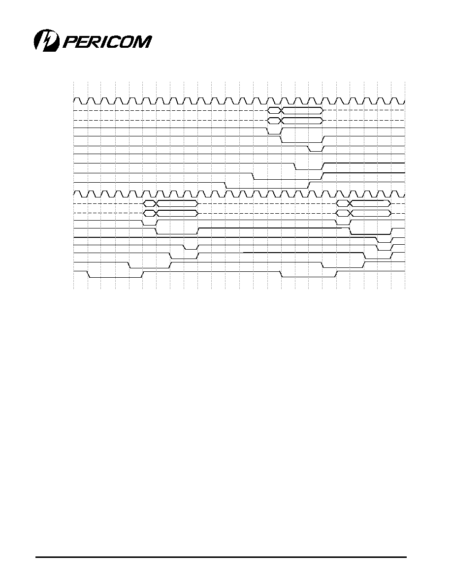
12345678901234567890123456789012123456789012345678901234567890121234567890123456789012345678901212345678901234567890123456789012123
12345678901234567890123456789012123456789012345678901234567890121234567890123456789012345678901212345678901234567890123456789012123
Appendix A
PI7C7100
3-Port PCI Bridge
A-17
04/18/00
ADVANCE INFORMATION
Addr
Data
Addr
Data
Byte Enables
Byte Enables
3
3
3
Addr
Data
Byte Enables
Figure 30. Upstream Delayed I/O Write Transaction ( S --> P )
0
1
2
3
4
5
6
7
8
9
10
11
12
13
14
15
16
17
18
19
20
21
22
0
1
2
3
4
5
6
7
8
9
10
11
12
13
14
15
16
17
18
19
20
21
22
P_CLK
P_AD [31:0]
P_CBE [3:0]
P_FRAME_L
P_IRDY_L
P_TRDY_L
P_STOP_L
P_DEVSEL_L
S_CLKOUT[0]
S_AD[31:0]
S_CBE[3:0]
S_FRAME_L
S_IRDY_L
S_TRDY_L
S_STOP_L
S_DEVSEL_L
S_GNT_L
S_REQ_L
P_GNT_L
P_REQ_L
23
23

A-18
04/18/00
123456789012345678901234567890121234567890123456789012345678901212345678901234567890123456789012123456789012345678901234567890121234
123456789012345678901234567890121234567890123456789012345678901212345678901234567890123456789012123456789012345678901234567890121234
Appendix A
PI7C7100
3-Port PCI Bridge
ADVANCE INFORMATION

PI7C7100
3-Port
PCI Bridge
Appendix B
Evaluation
Board
User's Manual

B-2
04/18/00
12345678901234567890123456789012123456789012345678901234567890121234567890123456789012345678901212345678901234567890123456789012123456
12345678901234567890123456789012123456789012345678901234567890121234567890123456789012345678901212345678901234567890123456789012123456
Appendix B
PI7C7100
3-Port PCI Bridge
ADVANCE INFORMATION
123456789012345678901234567890121234567890123456789012345678901212345678901234567890123456789012123456789012345678901234567890121234567
123456789012345678901234567890121234567890123456789012345678901212345678901234567890123456789012123456789012345678901234567890121234567
Appendix B
PI7C7100
3-Port PCI Bridge
B-3
04/18/00
ADVANCE INFORMATION
General Information
1.
Please make sure you have included with your PI7C7100 evaluation board, the five-page schematic and the
preliminary specification for the PI7C7100.
2.
Check all jumpers for proper settings:
PI7C7100 Evaluation Board User's Manual
3.
Check and make sure there are no shorts between power (3.3V, 5V, 12V, and 12V) and ground.
4.
Plug evaluation board in any PCI slot on your system. Make sure your system is powered off before doing so.
5.
Connect any PCI devices on the secondary slots of the evaluation board. Be careful that the orientation of the
card is correct (see Diagram A).
e
m
a
N
n
i
P
r
e
p
m
u
J
n
o
i
t
c
n
u
F
n
o
i
t
i
s
o
P
#
N
F
C
_
S
4
P
J
e
l
b
a
n
e
r
e
t
i
b
r
a
l
a
n
r
e
t
n
I
)
0
(
2
-
1
N
E
_
1
S
5
P
J
e
l
b
a
n
e
s
u
b
1
S
)
1
(
3
-
2
N
E
_
2
S
6
P
J
e
l
b
a
n
e
s
u
b
2
S
)
1
(
3
-
2
N
E
_
N
A
C
S
7
P
J
l
o
r
t
n
o
c
N
A
C
S
)
0
(
2
-
1
N
E
_
N
A
C
S
7
P
J
t
u
p
n
i
k
c
o
l
c
s
a
N
I
_
K
L
C
S
)
1
(
3
-
2
M
T
_
L
L
P
8
P
J
e
l
b
a
s
i
d
e
d
o
m
t
s
e
t
L
L
P
)
0
(
2
-
1
S
S
A
P
Y
B
9
P
J
e
l
b
a
s
i
d
L
L
P
)
1
(
3
-
2
#
H
S
U
L
F
_
P
0
1
P
J
e
l
b
a
s
i
d
h
s
u
l
f
O
F
I
F
y
r
a
m
i
r
P
)
1
(
3
-
2
PCI Add-In Card
Pericom
Semiconductor
Three-Port
PCI Bridge
Board
Diagram A

B-4
04/18/00
12345678901234567890123456789012123456789012345678901234567890121234567890123456789012345678901212345678901234567890123456789012123456
12345678901234567890123456789012123456789012345678901234567890121234567890123456789012345678901212345678901234567890123456789012123456
Appendix B
PI7C7100
3-Port PCI Bridge
ADVANCE INFORMATION
6.
Turn on the power for the system. Your OS should already have drivers for the PI7C7100 evaluation board.
In Win9X, Plug and Play should detect the device as a PCI-to-PCI bridge. The system may prompt you for the
Win9X CD for the drivers. The OS will detect two PCI-to-PCI bridges as the PI7C7100 has two secondary PCI
buses. In Win NT, you should not have to install drivers.
7.
Install drivers for any PCI devices you have attached to the evaluation board.
8.
If any of the steps are unclear or were unsuccessful, please contact your Pericom support person
at 408-435-0800.
9.
Thank you for evaluating Pericom Semiconductor Corporation's products.
General Information
(continued)

123456789012345678901234567890121234567890123456789012345678901212345678901234567890123456789012123456789012345678901234567890121234567
123456789012345678901234567890121234567890123456789012345678901212345678901234567890123456789012123456789012345678901234567890121234567
Appendix B
PI7C7100
3-Port PCI Bridge
B-5
04/18/00
ADVANCE INFORMATION
Frequently Asked Questions
1.
What is the function of SCAN_EN?
SCAN_EN is for a full scan test or S_CLKIN select. During SCAN mode, SCAN_EN will be driven to logic "0"
or "logic "1" depending on functionality. During normal mode, if SCAN_EN is connected to logic "0" (JP7 in
the 1-2 position), S_CLKIN will be used for PLL test only when PL_TM is active. If SCAN_EN is connected to
logic "1" (JP7 in the 2-3 position), S_CLKIN will be the clock input for the secondary buses. All secondary
clock outputs, S_CLKOUT [15:0], are still derived from P_CLK with 0-10ns delay. The S_CLKOUT [15:0]
should be disabled by programming the bits [15:0] in both configuration registers 1 and 2 at offset 68h.
2.
What is the function of SCAN_TM#?
SCAN_TM# is for full scan test and power on reset for the PLL. SCAN_TM# should be connected to logic "1" or
to an RC path (R1 and C13) during normal operation.
3.
How do you use the external arbiter?
a)
Disable the on chip arbiter by connecting S_CFN to logic "1" (JP4 in the 2-3 position).
b)
Use S1_REQ0# as GRANT and S1_GNT0# as REQUEST on the S1 bus.
c)
Use S2_REQ0# as GRANT and S2_GNT0# as REQUEST on the S2 bus.
4.
What is the purpose of having JP1, JP2, and JP3?
JP1, JP2, and JP3 are designed for easy access to the primary bus signals. You may connect any of these pins
to an oscilloscope or a logic analyzer for observation. No connection is required for normal operation. The
following table indicates which bus signals correspond to which pins.
5.
What is the purpose for having U17, U19, and U20?
U17, U19, and U20 are designed for easy access to the digital ground planes for observation.
6.
How is the evaluation board constructed?
The evaluation board is a six-layer PCB. The top and bottom layers (1 and 6) are for signals, power, and ground
routing. Layer 2 and layer 5 are ground planes. Layer 3 is a digital 3.3V power plane. Layer 4 is a digital 5V
power plane with an island of analog 3.3V power.
7.
What is the function of S_CLKIN?
The S_CLKIN pin is a test pin for the on chip PLL when PLL_TM is set to logic "1". During normal operation, if
PLL_TM is set to logic "0", SCAN_TM# is set to logic "1", and SCAN_EN is set to logic "1", then S_CLKIN will
be the clock input for both the secondary buses. However, the S_CLKOUT [15:0] are still derived by program-
ming bits [15:0] in both configuration registers 1 and 2 at offset 68h.
8.
What clock frequency combinations does the PI7C7100 support?
Primary Bus
Secondary (1 and 2) Buses
33MHz
33MHz
9.
How are the JTAG signals being connected?
The JTAG signals consist of TRST#, TCK, TMS, TDI, and TDO. All the mentioned signals have weak internal
pull-up connections. Therefore, no connection is needed if you want the JTAG circuit to be disabled. If you want
to activate the JTAG circuit, you need to connect all five signals according to the JTAG specification (IEEE
1149).
1
2
3
4
5
6
7
8
9
0
1
1
1
2
1
3
1
4
1
5
1
6
1
2
P
J
Q
E
R
9
2
D
A
6
2
D
A
3
E
B
C
1
2
D
A
8
1
D
A
2
E
B
C
Y
D
R
I
K
C
O
L
R
A
P
4
1
D
A
1
1
D
A
0
E
B
C
6
D
A
5
D
A
0
D
A
3
P
J
1
3
D
A
8
2
D
A
5
2
D
A
3
2
D
A
0
2
D
A
7
1
D
A
E
M
A
R
F
L
E
S
V
D
R
R
E
P
1
E
B
C
3
1
D
A
0
1
D
A
8
D
A
4
D
A
2
D
A
D
N
G
1
P
J
T
N
G
0
3
D
A
7
2
D
A
4
2
D
A
2
2
D
A
9
1
D
A
6
1
D
A
Y
D
R
I
P
O
T
S
R
R
E
S
5
1
D
A
2
1
D
A
9
D
A
7
D
A
3
D
A
1
D
A

B-6
04/18/00
12345678901234567890123456789012123456789012345678901234567890121234567890123456789012345678901212345678901234567890123456789012123456
12345678901234567890123456789012123456789012345678901234567890121234567890123456789012345678901212345678901234567890123456789012123456
Appendix B
PI7C7100
3-Port PCI Bridge
ADVANCE INFORMATION

PI7C7100
3-Port
PCI Bridge
Appendix C
Schematics

C-2
04/18/00
12345678901234567890123456789012123456789012345678901234567890121234567890123456789012345678901212345678901234567890123456789012123456
12345678901234567890123456789012123456789012345678901234567890121234567890123456789012345678901212345678901234567890123456789012123456
Appendix C
PI7C7100
3-Port PCI Bridge
ADVANCE INFORMATION
123456789012345678901234567890121234567890123456789012345678901212345678901234567890123456789012123456789012345678901234567890121234567
123456789012345678901234567890121234567890123456789012345678901212345678901234567890123456789012123456789012345678901234567890121234567
C-3
04/18/00
Appendix C
PI7C7100
3-Port PCI Bridge
ADVANCE INFORMATION
A
A
B
B
C
C
D
D
E
E
4
4
3
3
2
2
1
1
JP4
JP5
JP6
JP7
JP8
JP9
JP10
JP Select
Name
S_CFNn
Internal
Arbiter
Function
S1_EN
S2_EN
S1_Enable
S2_Enable
Position
1-2
2-3
2-3
SCAN_EN
1-2
SCAN
Disable
PLL_TM
1-2
PLL_TM
Disable
ByPass_L
PLL
Enable
1-2
P_Flush_L
P_Flush
Disable
2-3
PI7C7100
1.3
Three Port PCI Bridge Evaluation Board
C
15
Friday, March 17, 2000
2380 Bering Dr., San Jose,
C
A
PCI Chip
Title
Size
Document Number
Rev
Date:
Sheet
of
P_AD13
S1_AD2
S1_CBE3
P_AD9
P_AD14
S1_AD20
P_PERRN
P_AD7
P_AD17
P_AD18
P_AD31
S1_AD3
S1_AD5
S1_AD8
S1_AD13
S1_AD18
S1_AD28
P_AD22
S1_AD24
S1_AD25
P_AD8
S1_AD16
S1_CBE2
P_AD15
P_AD28
P_CBE1
S1_AD9
S1_AD12
S1_AD[31:0]
S1_AD0
S1_AD30
P_AD0
P_AD4
P_AD26
S1_AD29
S1_CBE1
P_M66EN
P_LOCKN
P_AD10
P_AD30
S1_AD11
S1_AD14
S1_AD21
P_AD23
P_AD27
P_CBE0
S1_AD6
S1_AD10
P_AD25
P_CBE3
S1_AD17
P_AD1
P_AD3
P_AD12
S1_AD7
S1_AD15
S1_AD19
S1_CBE0
P_AD19
S1_AD1
S1_AD23
P_AD11
P_AD16
P_AD21
P_AD[31:0]
S1_AD4
S1_AD22
P_AD2
P_AD5
P_AD29
S1_AD27
S1_AD[31:0]
S1_AD31
S_M66EN
P_CBE2
P_SERRN
P_AD6
P_AD20
P_AD24
S1_AD26
ByPass
S1_FRAMEN
S1_GNTN0
S1_DEVSELN
S1_REQN4
S1_GNTN2
S1_GNTN4
S1_LOCKN
S1_GNTN6
S1_REQN3
S1_REQN5
S1_REQN7
S1_GNTN1
S1_REQN1
S1_GNTN5
S1_GNTN3
S1_GNTN7
S1_IRDYN
S1_REQN2
S1_REQN0
S1_PAR
S1_REQN6
S2_AD[31:0]
S2_AD13
S2_AD3
S2_AD19
S2_AD22
S2_AD0
S2_AD9
S2_AD10
S2_AD21
S2_AD28
S2_CBE0
S2_AD15
S2_AD27
S2_CBE3
S2_AD25
S2_AD30
S2_AD2
S2_AD11
S2_AD12
S2_AD14
S2_CBE2
S2_AD18
S2_AD20
S2_AD23
S2_AD5
S2_CBE1
S2_AD17
S2_AD29
S2_AD31
S2_AD8
S2_AD4
S2_AD6
S2_AD7
S2_AD16
S2_AD26
S2_AD1
S2_AD24
S2_GNTN1
S2_REQN2
S2_GNTN7
S2_REQN7
S2_GNTN2
S2_GNTN4
S2_REQN1
S2_GNTN5
S2_REQN3
S2_GNTN3
S2_REQN5
S2_REQN4
S2_REQN6
S2_GNTN0
S2_GNTN6
S2_REQN0
SCLKOUT0
SCLKOUT13
SCLKOUT5
SCLKOUT6
SCLKOUT11
SCLKOUT14
SCLKOUT4
SCLKOUT9
SCLKOUT1
SCLKOUT2
SCLKOUT12
SCLKOUT15
SCLKOUT3
SCLKOUT8
SCLKOUT7
SCLKOUT10
+3.3V
+3.3V
+3.3V
+3.3V
+3.3V
+3.3V
+3.3V
+3.3V
+3.3V
AVCC
+3.3V
+3.3V
AVCC
AVCC
+3.3V
AVCC
+5V
AVCC
+3.3V
+3.3V
+3.3V
+3.3V
R11
5.1K
R9
5.1k
R1
3.3k
R2
5.1K
R6
5.1k
C13
0.1uF
R4
5.1k
R8
5.1K
JP4
HEADER 3
1
2
3
R3
5.1K
R7
5.1k
JP5
HEADER 3
1
2
3
JP6
HEADER 3
1
2
3
JP7
HEADER 3
1
2
3
R12
5.1K
R10
5.1k
JP8
HEADER 3
1
2
3
R13
5.1k
R14
5.1K
JP9
HEADER 3
1
2
3
C58
0.01uF
F3A
1
2
C55
0.001uF
C59
0.1uF
C19
0.001uF
C42
0.001uF
C57
0.1uF
C41
0.1uF
C60
0.001uF
C56
0.01uF
C40
0.01uF
C22
0.01uF
C23
0.1uF
R15
5.1K
JP10
HEADER 3
1
2
3
R16
5.1k
C45
0.1uF
C44
0.01uF
C47
0.1uF
C46
0.01uF
C48
0.001uF
C43
0.001uF
F3A
1
2
C50
0.01uF
C51
0.1uF
C49
0.001uF
+
C8
10uF
+
C10
10uF
+
C9
10uF
C12
0.1uF
C11
0.01uF
C353
0.001uF
C371
0.1uF
C370
0.01uF
C372
0.001uF
C373
0.01uF
+
C374
10uF
U0
LT11
17
GND
1
VO
2
VI
3
TAB
4
C354
100uF
+
C7
10uF
C16
0.1uF
C17
0.1uF
R5
121
R17
0
R18
150
R25
226
C24
0.01uF
C25
0.01uF
C26
0.01uF
C27
0.01uF
C28
0.01uF
C29
0.01uF
C21
0.001uF
C20
0.001uF
C38
0.001uF
C39
0.001uF
C30
0.001uF
C31
0.001uF
C36
0.1uF
C34
0.1uF
C37
0.1uF
C33
0.1uF
C35
0.1uF
C32
0.1uF
C360
0.01uF
C367
0.001uF
C363
0.01uF
C365
0.1uF
C361
0.001uF
C368
0.1uF
C366
0.01uF
C362
0.1uF
C364
0.001uF
t1
Table1
U1
PI7C7100
P_AD[0]
R17
P_AD[1]
T17
P_AD[2]
Y20
P_AD[3]
V20
P_AD[4]
U20
P_AD[5]
Y19
P_AD[6]
W19
P_AD[7]
U19
P_AD[8]
Y18
P_AD[9]
W18
P_AD[10]
U18
P_AD[11]
Y17
P_AD[12]
W17
P_AD[13]
Y16
P_AD[14]
W16
P_AD[25]
Y9
P_AD[16]
V12
P_AD[17]
W12
P_AD[18]
Y12
P_AD[19]
U11
P_AD[20]
V11
P_AD[21]
Y11
P_AD[22]
V10
P_AD[23]
W10
P_AD[24]
W9
P_AD[15]
V16
P_AD[26]
U8
P_AD[27]
V8
P_AD[28]
W8
P_AD[29]
Y8
P_AD[30]
W7
P_AD[31]
Y7
P_CBE[0]
V19
P_CBE[1]
U16
P_CBE[2]
U12
P_CBE[3]
V9
S_CFN_L
Y2
AGND
U4
AVCC
Y1
S1_AD[0]
T19
S1_AD[1]
T20
S1_AD[2]
R18
S1_AD[3]
R19
S1_AD[4]
R20
S1_AD[5]
P17
S1_AD[6]
N17
S1_AD[7]
N18
S1_AD[8]
N19
S1_AD[9]
N20
S1_AD[10]
M17
S1_AD[11]
M19
S1_AD[12]
M20
S1_AD[13]
L18
S1_AD[14]
L19
S1_AD[15]
L20
S1_AD[16]
G19
S1_AD[17]
G20
S1_AD[18]
F17
S1_AD[19]
F19
S1_AD[20]
F20
S1_AD[21]
E17
S1_AD[22]
E18
S1_AD[23]
E19
S1_AD[24]
D17
S1_AD[25]
D19
S1_AD[26]
D20
S1_AD[27]
C18
S1_AD[28]
C19
S1_AD[29]
C20
S1_AD[30]
B19
S1_AD[31]
B20
S1_CBE[0]
P20
S1_CBE[1]
K17
S1_CBE[2]
G18
S1_CBE[3]
E20
DGND
C2
S2_EN
W4
JTAG_TCK
V2
JTAG_TMS
W1
JTAG_TD0
V3
JTAG_TDI
W2
SCAN_TM_L
V4
SCAN_EN_H
U5
PLL_TM_H
Y3
CMPO1
U6
RESERVED
R4
ByPass
Y4
P_M66EN
V18
PLL_SCLK
V5
S_M66EN
D7
PLL_PCLK
V6
P_FLUSH_L
W5
P_RESET_L
Y5
P_GNT
U7
P_IDSEL
Y10
P_REQ
W6
P_FRAME_L
W13
P_IRDY_L
V13
P_TRDY_L
U13
P_DEVSEL_L
Y14
P_STOP_
L
W14
P_LOCK_L
V14
P_PERR_L
Y15
P_SERR_L
W15
P_PAR
U15
TRST_L
U3
S1_EN
W3
+D3.3V
E2
+D3.3V
J3
+D3.3V
N2
+D3.3V
V1
+D3.3V
V7
+D3.3V
U10
+D3.3V
V15
+D3.3V
W20
+D3.3V
P19
+D3.3V
L17
+D3.3V
F18
+D3.3V
D15
+D3.3V
C14
+D3.3V
D11
+D3.3V
B8
+D3.3V
D5
DGND
E3
DGND
G2
DGND
J2
DGND
K4
DGND
N1
DGND
R2
DGND
U2
DGND
Y6
DGND
U9
DGND
W11
DGND
Y13
DGND
U14
DGND
V17
DGND
U17
DGND
T18
DGND
P18
DGND
M18
DGND
K19
DGND
H17
DGND
G17
DGND
D18
DGND
A20
DGND
A17
DGND
A15
DGND
D12
DGND
A10
DGND
A8
DGND
A5
DGND
A3
S1_DEVSEL_L
J20
S1_FRAME_L
H20
S1_GNTN[0]
B18
S1_GNTN[1]
D16
S1_GNTN[2]
B16
S1_GNTN[3]
D14
S1_GNTN[4]
A14
S1_GNTN[5]
B13
S1_GNTN[6]
B12
S1_GNTN[7]
C11
S1_IRDY_L
H19
S1_LOCK_L
J18
S1_PAR_L
K18
S1_PERR_L
J17
S1_REQ[0]
B17
S1_REQ[1]
C17
S1_REQ[2]
A16
S1_REQ[3]
C15
S1_REQ[4]
C13
S1_REQ[5]
D13
S1_REQ[6]
A12
S1_REQ[7]
B11
S1_RESET_L
B10
S1_SERR_L
K20
S1_STOP_L
J19
S1_TRDY_L
H18
S2_AD[0]
C10
S2_AD[1]
D10
S2_AD[2]
A9
S2_AD[3]
B9
S2_AD[4]
C9
S2_AD[5]
D9
S2_AD[6]
C8
S2_AD[7]
D8
S2_AD[8]
B7
S2_AD[9]
C7
S2_AD[10]
A6
S2_AD[11]
B6
S2_AD[12]
C6
S2_AD[13]
D6
S2_AD[14]
B5
S2_AD[15]
C5
S2_AD[16]
B1
S2_AD[17]
C1
S2_AD[18]
D1
S2_AD[19]
E4
S2_AD[20]
E1
S2_AD[21]
F4
S2_AD[22]
F3
S2_AD[23]
F2
S2_AD[24]
G4
S2_AD[25]
G3
S2_AD[26]
G1
S2_AD[27]
H4
S2_AD[28]
H3
S2_AD[29]
H2
S2_AD[30]
H1
S2_AD[31]
J4
S2_CBE[0]
A7
S2_CBE[1]
A4
S2_CBE[2]
A1
S2_CBE[3]
F1
S2_DEVSEL_L
D3
S2_FRAME_L
D2
S2_GNTN[0]
K2
S2_GNTN[1]
L1
S2_GNTN[2]
L4
S2_GNTN[3]
M3
S2_GNTN[4]
N4
S2_GNTN[5]
R1
S2_GNTN[6]
P4
S2_GNTN[7]
U1
S2_IRDY_L
B2
S2_LOCK_L
B3
S2_PAR_L
B4
S2_PERR_L
D4
S2_REQ[0]
K3
S2_REQ[1]
K1
S2_REQ[2]
M1
S2_REQ[3]
M2
S2_REQ[4]
P1
S2_REQ[5]
P2
S2_REQ[6]
R3
S2_REQ[7]
T2
S2_RESET_L
T4
S2_SERR_L
C4
S2_STOP_L
C3
S2_TRDY_L
A2
SCLKOUT[15]
T3
SCLKOUT[14]
T1
SCLKOUT[13]
P3
SCLKOUT[12]
N3
SCLKOUT[11]
M4
SCLKOUT[10]
L3
SCLKOUT[9]
L2
SCLKOUT[8]
J1
SCLKOUT[7]
A11
SCLKOUT[6]
C12
SCLKOUT[5]
A13
SCLKOUT[4]
B14
SCLKOUT[3]
B15
SCLKOUT[2]
C16
SCLKOUT[1]
A18
SCLKOUT[0]
A19
S1_AD[31:0]
P_CBE[3:0]
P_AD[31:0]
S1_CBE[3:0]
PLL_PCLK
TDO
S_M66EN
P_DEVSELN
P_RESETN
P_REQN
TCK
P_IRDYN
P_SERRN
P_M66EN
P_FRAMEN
TM
S
PLL_SCLK
P_IDSEL
TDI
PLL_CAP1
P_TRDYN
P_STOPN
TRST_L
P_GNTN
P_LOCKN
PLL_CAP2
P_PERRN
P_PAR
S1_REQN[7:0]
S1_GNTN[7:0]
S1_STOPN
S1_FRAMEN
S1_LOCKN
S1_PERRN
S1_SERRN
S1_IRDYN
S1_RESETN
S1_PAR
S1_DEVSELN
S1_TRDYN
S2_CBE[3:0]
S2_AD[31:0]
S2_REQN[7:0]
S2_GNTN[7:0]
S2_IRDYN
S2_STOPN
S2_RESETN
S2_DEVSELN
S2_PERRN
S2_TRDYN
S2_PAR
S2_LOCKN
S2_SERRN
S2_FRAMEN
SCLKOUT[15:0]
C-4
04/18/00
12345678901234567890123456789012123456789012345678901234567890121234567890123456789012345678901212345678901234567890123456789012123456
12345678901234567890123456789012123456789012345678901234567890121234567890123456789012345678901212345678901234567890123456789012123456
Appendix C
PI7C7100
3-Port PCI Bridge
ADVANCE INFORMATION
A
A
B
B
C
C
D
D
E
E
4
4
3
3
2
2
1
1
JP1 GNT AD30 AD27 AD24 AD22 AD19 AD16 IRDY STOP SERR AD15 AD12 AD9 AD7 AD3 AD1
JP3 AD31 AD28 AD25 AD23 AD20 AD17 Frame DVSEL PERR CBE1 AD13 AD10 AD8 AD4 AD2 GND
JP2 REQ AD29 AD26 CBE3 AD21 AD18 CBE2 TRDY LOCK PAR AD14 AD11 CBE0 AD6 AD5 AD0
1 2 3 4 5 6 7 8 9 10 11 12 13 14 15 16
PI7C7100
1.3
Three Port PCI Bridge Evaluation Board
C
25
Friday, March 17, 2000
2380 Bering Dr., San Jose,
C
A
P
C
I
Edge Connector
Title
Size
Document Number
Rev
Date:
Sheet
of
INTA
INTB
P_RESET_L
AD31
AD30
AD29
AD28
AD27
AD26
AD25
AD23
AD20
AD18
AD17
AD16
C/BE2
C/BE1
AD0
M66EN
AD[31:0]
C/BE[3:0]
INTC
AD24
P_IDSEL_L
AD22
AD15
AD13
AD11
AD9
C/BE0
AD6
AD4
AD2
INTD
P_CLK
C/BE3
AD21
AD19
AD12
AD10
AD8
AD7
AD5
AD3
AD1
P_REQ_L
P_GNT_L
P_GNT_L
P_REQ_L
AD31
AD30
P_PERR_L
AD29
AD28
AD27
AD26
AD24
AD25
C/BE3
AD23
AD22
AD21
AD20
AD19
AD18
AD17
AD16
C
/BE2
P_FRAME_L
P_FRAME_L
P_IRDY_L
P_IRDY_L
P_TRDY_L
P_TRDY_L
P_DVSEL_L
P_DVSEL_L
P_STOP_
L
P_STOP_
L
P_LOCK_L
P_SERR_L
P_LOCK_L
P_PERR_L
P_SERR_L
P_PAR
P_PAR
C/BE1
AD15
AD14
AD14
AD13
AD12
AD11
AD10
AD9
C/BE0
AD8
AD7
AD6
AD5
AD4
AD3
AD2
AD1
AD0
INTA
INTC
INTB
INTD
+12V
-12V
+5VIO1
+5V
+3.3V
+3.3V
+5V
+5VIO2
+3.3V
C103
0.01uF
C104
0.01uF
C111
0.1uF
C112
0.01uF
+
C102
10uF
+
C101
10uF
C117
0.01uF
R31
5
.1k
R32
5
.1k
R27
0
R29
0
R26
0
R28
0
R30
0
C110
0.01uF
U38
1header
T
1
C113
0.1uF
C114
0.1uF
C115
0.01uF
C116
0.01uF
C1
0.1uF
C6
0.001uF
C14
0.001uF
C15
0.001uF
C18
0.001uF
JP1
HEADER 16
1
2
3
4
5
6
7
8
9
10
11
12
13
14
15
16
JP2
HEADER 16
1
2
3
4
5
6
7
8
9
10
11
12
13
14
15
16
JP3
HEADER 16
1
2
3
4
5
6
7
8
9
10
11
12
13
14
15
16
U5
PCIEDGE
TRST#
A1
+12V
A2
TMS
A3
TDI
A4
+5V
A5
INTA#
A6
INTC#
A7
+5V
A8
NC
A9
+5VIO1
A10
NC
A11
NC
A14
RST#
A15
+5VIO1
A16
GNT#
A17
GND
A18
NC
A19
AD30
A20
+3.3V
A21
AD28
A22
AD26
A23
GND
A24
AD24
A25
IDSEL
A26
+3.3V
A27
AD22
A28
AD20
A29
GND
A30
AD18
A31
AD16
A32
+3.3V
A33
FRAME#
A34
GND
A35
TRDY#
A36
GND
A37
STOP#
A38
+3.3V
A39
SDONE
A40
SBO#
A41
GND
A42
PAR
A43
AD15
A44
+3.3V
A45
AD13
A46
AD11
A47
GND
A48
AD09
A49
NC
A50
NC
A51
C/BE0#
A52
+3.3V
A53
AD06
A54
AD04
A55
GND
A56
AD02
A57
AD00
A58
+5VIO2
A59
REQ64#
A60
+5V
A61
+5V
A62
-12V
B1
TCK
B2
GND
B3
TDO
B4
+5V
B5
+5V
B6
INTB#
B7
INTD#
B8
PRSNT1#
B9
NC
B10
PRSNT2#
B11
NC
B12
NC
B14
GND
B15
CLK
B16
GND
B17
REQ#
B18
+5VIO1
B19
AD31
B20
AD29
B21
GND
B22
AD27
B23
AD25
B24
+3.3V
B25
C/BE3#
B26
AD23
B27
GND
B28
AD21
B29
AD19
B30
+3.3V
B31
AD17
B32
C/BE2#
B33
GND
B34
IRDY#
B35
+3.3V
B36
DEVSEL#
B37
GND
B38
LOCK#
B39
PERR#
B40
+3.3V
B41
SERR#
B42
+3.3V
B43
C/BE1#
B44
AD14
B45
GND
B46
AD12
B47
AD10
B48
M66EN
B49
NC
B50
NC
B51
AD08
B52
AD07
B53
+3.3V
B54
AD05
B55
AD03
B56
GND
B57
AD01
B58
+5VIO2
B59
ACK64#
B60
+5V
B61
+5V
B62
NC
B13
NC
A12
NC
A13
C121
0.001uF
C2
0.01uF
C106
0.1uF
+
C97
10uF
C119
0.001uF
C108
0.01uF
C5
0.1uF
C3
0.1uF
+
C109
10uF
U40
1header
T
1
U44
1header
T
1
U42
1header
T
1
U43
1header
T
1
U41
1header
T
1
U39
1header
T
1
U48
1header
T
1
U47
1header
T
1
U46
1header
T
1
U45
1header
T
1
C120
0.001uF
C105
0.01uF
C107
0.01uF
C4
0.1uF
C118
0.001uF
T2
Table2
IRDY_L
LOCK_L
FRAME_L
TRDY_L
STOP_
L
PAR
DVSEL_L
INTB_L
INTD_L
RESET_L
INTA_L
INTC_L
CLK
TCK
TM
S
TRST_L
IDSEL_L
SERR_L
M66EN
REQ_L
TDI
TDO
AD[31:0]
C/BE[3:0]
GNT_L
PERR_L
123456789012345678901234567890121234567890123456789012345678901212345678901234567890123456789012123456789012345678901234567890121234567
123456789012345678901234567890121234567890123456789012345678901212345678901234567890123456789012123456789012345678901234567890121234567
C-5
04/18/00
Appendix C
PI7C7100
3-Port PCI Bridge
ADVANCE INFORMATION
A
A
B
B
C
C
D
D
E
E
4
4
3
3
2
2
1
1
PI7C7100
1.3
Three Port PCI Bridge Evaluation Board
C
35
Friday, March 17, 2000
2380 Bering Dr., San Jose,
C
A
Secondary 1 P
C
I
B
u
s
Title
Size
Document Number
Rev
Date:
Sheet
of
AD31
AD30
AD29
AD28
AD27
AD26
AD25
AD24
C/BE3
AD23
AD22
AD21
AD20
AD19
AD18
AD17
AD16
C/BE2
SERR_L
C/BE1
AD15
AD14
AD13
AD12
AD11
AD10
AD9
AD8
C/BE0
AD7
AD6
AD5
AD4
AD3
AD2
AD1
AD0
M66EN
TCK0
TRST0_L
TMS
0
TDI0
AD31
AD30
AD29
AD28
AD27
AD26
AD25
AD24
C/BE3
AD23
AD22
AD21
AD20
AD19
AD18
AD17
AD16
C/BE2
SERR_L
C/BE1
AD15
AD14
AD13
AD12
AD11
AD10
AD9
AD8
C/BE0
AD7
AD6
AD5
AD4
AD3
AD2
AD1
AD0
M66EN
TCK1
TRST1_L
TMS
1
TDI1
AD31
AD30
AD29
AD28
AD27
AD26
AD25
AD24
C/BE3
AD23
AD22
AD21
AD20
AD19
AD18
AD17
AD16
C/BE2
SERR_L
C/BE1
AD15
AD14
AD13
AD12
AD11
AD10
AD9
AD8
C/BE0
AD7
AD6
AD5
AD4
AD3
AD2
AD1
AD0
M66EN
TCK2
TRST2_L
TMS
2
TDI2
SBO2_
L
SBO1_
L
SBO0_
L
SBO0_
L
SDONE0
SBO1_
L
SDONE1
SBO2_
L
SDONE2
SBO3_
L
SDONE0
SDONE2
SDONE1
SDONE3
M66EN
AD[31:0]
C/BE[3:0]
REQ64#2
ACK64#2
ACK64#0
REQ64#0
ACK64#1
REQ64#1
ACK64#0
ACK64#1
REQ64#0
REQ64#1
ACK64#2
REQ64#2
REQ64#3
ACK64#3
TRDY_L
FRAME_L
IRDY_L
DEVSEL_L
PERR_L
SERR_L
LOCK_L
STOP_
L
AD31
AD30
AD29
AD28
AD27
AD26
AD25
AD24
C/BE3
AD23
AD22
AD21
AD20
AD19
AD18
AD17
AD16
C/BE2
SERR_L
C/BE1
AD15
AD14
AD13
AD12
AD11
AD10
AD9
AD8
C/BE0
AD7
AD6
AD5
AD4
AD3
AD2
AD1
AD0
M66EN
TRST3_L
TMS
3
TDI3
SBO3_
L
SDONE3
REQ64#3
ACK64#3
TCK3
+3.3V
+3.3V
+12V
-12V
+3.3V
+3.3V
+12
V
-12V
+3.3V
+12
V
+3.3V
+5V
-12V
+5V
+3.3V
+3.3V
+3.3V
+3.3V
+3.3V
+3.3V
+3.3V
+3.3V
+5V
+3.3V
+3.3V
+5V
+12
V
+5V
+5V
-12V
C150
0.01uF
C149
0.01uF
C152
0.01uF
R72
5.1K
1
2
R60
5.1K
1
2
R53
5.1K
1
2
R66
5.1K
1
2
R71
5.1K
1
2
R52
5.1K
1
2
R59
5.1K
1
2
R65
5.1K
1
2
C153
0.01uF
C154
0.01uF
C161
0.01uF
C162
0.01uF
C163
0.01uF
C164
0.01uF
C165
0.01uF
C166
0.01uF
C167
0.01uF
C186
0.1uF
C189
0.1uF
C185
0.01uF
C187
0.1uF
C184
0.01uF
C190
0.1uF
C188
0.1uF
C211
0.01uF
C214
0.01uF
C218
0.01uF
C210
0.01uF
C217
0.01uF
C212
0.01uF
C209
0.01uF
C219
0.01uF
+
C204
10uF
+
C206
10uF
C220
0.01uF
C215
0.01uF
C213
0.01uF
C131
0.1uF
C134
0.1uF
C138
0.1uF
C132
0.1uF
C139
0.1uF
C140
0.1uF
C135
0.1uF
C133
0.1uF
R37
5.1K
1
2
R38
5.1K
1
2
R39
5.1K
1
2
R34
5.1K
1
2
R35
5.1K
1
2
R36
5.1K
1
2
R42
5.1K
1
2
R45
5.1K
1
2
R41
5.1K
1
2
R44
5.1K
1
2
R40
5.1K
1
2
R43
5.1K
1
2
R70
5.1K
1
2
R58
5.1K
1
2
R51
5.1K
1
2
R64
5.1K
1
2
R69
5.1K
1
2
R50
5.1K
1
2
R57
5.1K
1
2
R63
5.1K
1
2
R74
5.1K
1
2
R55
5.1K
1
2
R62
5.1K
1
2
R68
5.1K
1
2
R67
5.1K
1
2
R61
5.1K
1
2
R54
5.1K
1
2
R73
5.1K
1
2
U10
PCISLOT
TRST#
A1
+12V
A2
TMS
A3
TDI
A4
+5V
A5
INTA#
A6
INTC#
A7
+5V
A8
NC
A9
+5V
A10
NC
A11
GND
A12
GND
A13
NC
A14
RST#
A15
+5V
A16
GNT#
A17
GND
A18
NC
A19
AD30
A20
+3.3V
A21
AD28
A22
AD26
A23
GND
A24
AD24
A25
IDSEL
A26
+3.3V
A27
AD22
A28
AD20
A29
GND
A30
AD18
A31
AD16
A32
+3.3V
A33
FRAME#
A34
GND
A35
TRDY#
A36
GND
A37
STOP#
A38
+3.3V
A39
SDONE
A40
SBO#
A41
GND
A42
PAR
A43
AD15
A44
+3.3V
A45
AD13
A46
AD11
A47
GND
A48
AD09
A49
NC
A50
NC
A51
C/BE0#
A52
+3.3V
A53
AD06
A54
AD04
A55
GND
A56
AD02
A57
AD00
A58
+5V
A59
REQ64#
A60
+5V
A61
+5V
A62
-12V
B1
TCK
B2
GND
B3
TDO
B4
+5V
B5
+5V
B6
INTB#
B7
INTD#
B8
PRSNT1#
B9
NC
B10
PRSNT2#
B11
GND
B12
GND
B13
NC
B14
GND
B15
CLK
B16
GND
B17
REQ#
B18
+5V
B19
AD31
B20
AD29
B21
GND
B22
AD27
B23
AD25
B24
+3.3V
B25
C/BE3#
B26
AD23
B27
GND
B28
AD21
B29
AD19
B30
+3.3V
B31
AD17
B32
C/BE2#
B33
GND
B34
IRDY#
B35
+3.3V
B36
DEVSEL#
B37
GND
B38
LOCK#
B39
PERR#
B40
+3.3V
B41
SERR#
B42
+3.3V
B43
C/BE1#
B44
AD14
B45
GND
B46
AD12
B47
AD10
B48
M66EN
B49
NC
B50
NC
B51
AD08
B52
AD07
B53
+3.3V
B54
AD05
B55
AD03
B56
GND
B57
AD01
B58
+5V
B59
ACK64#
B60
+5V
B61
+5V
B62
U9
PCISLOT
TRST#
A1
+12V
A2
TMS
A3
TDI
A4
+5V
A5
INTA#
A6
INTC#
A7
+5V
A8
NC
A9
+5V
A10
NC
A11
GND
A12
GND
A13
NC
A14
RST#
A15
+5V
A16
GNT#
A17
GND
A18
NC
A19
AD30
A20
+3.3V
A21
AD28
A22
AD26
A23
GND
A24
AD24
A25
IDSEL
A26
+3.3V
A27
AD22
A28
AD20
A29
GND
A30
AD18
A31
AD16
A32
+3.3V
A33
FRAME#
A34
GND
A35
TRDY#
A36
GND
A37
STOP#
A38
+3.3V
A39
SDONE
A40
SBO#
A41
GND
A42
PAR
A43
AD15
A44
+3.3V
A45
AD13
A46
AD11
A47
GND
A48
AD09
A49
NC
A50
NC
A51
C/BE0#
A52
+3.3V
A53
AD06
A54
AD04
A55
GND
A56
AD02
A57
AD00
A58
+5V
A59
REQ64#
A60
+5V
A61
+5V
A62
-12V
B1
TCK
B2
GND
B3
TDO
B4
+5V
B5
+5V
B6
INTB#
B7
INTD#
B8
PRSNT1#
B9
NC
B10
PRSNT2#
B11
GND
B12
GND
B13
NC
B14
GND
B15
CLK
B16
GND
B17
REQ#
B18
+5V
B19
AD31
B20
AD29
B21
GND
B22
AD27
B23
AD25
B24
+3.3V
B25
C/BE3#
B26
AD23
B27
GND
B28
AD21
B29
AD19
B30
+3.3V
B31
AD17
B32
C/BE2#
B33
GND
B34
IRDY#
B35
+3.3V
B36
DEVSEL#
B37
GND
B38
LOCK#
B39
PERR#
B40
+3.3V
B41
SERR#
B42
+3.3V
B43
C/BE1#
B44
AD14
B45
GND
B46
AD12
B47
AD10
B48
M66EN
B49
NC
B50
NC
B51
AD08
B52
AD07
B53
+3.3V
B54
AD05
B55
AD03
B56
GND
B57
AD01
B58
+5V
B59
ACK64#
B60
+5V
B61
+5V
B62
C226
0.01uF
C194
0.1uF
C195
0.1uF
C74
0.1uF
C69
0.1uF
C70
0.1uF
U11
PCISLOT
TRST#
A1
+12V
A2
TMS
A3
TDI
A4
+5V
A5
INTA#
A6
INTC#
A7
+5V
A8
NC
A9
+5V
A10
NC
A11
GND
A12
GND
A13
NC
A14
RST#
A15
+5V
A16
GNT#
A17
GND
A18
NC
A19
AD30
A20
+3.3V
A21
AD28
A22
AD26
A23
GND
A24
AD24
A25
IDSEL
A26
+3.3V
A27
AD22
A28
AD20
A29
GND
A30
AD18
A31
AD16
A32
+3.3V
A33
FRAME#
A34
GND
A35
TRDY#
A36
GND
A37
STOP#
A38
+3.3V
A39
SDONE
A40
SBO#
A41
GND
A42
PAR
A43
AD15
A44
+3.3V
A45
AD13
A46
AD11
A47
GND
A48
AD09
A49
NC
A50
NC
A51
C/BE0#
A52
+3.3V
A53
AD06
A54
AD04
A55
GND
A56
AD02
A57
AD00
A58
+5V
A59
REQ64#
A60
+5V
A61
+5V
A62
-12V
B1
TCK
B2
GND
B3
TDO
B4
+5V
B5
+5V
B6
INTB#
B7
INTD#
B8
PRSNT1#
B9
NC
B10
PRSNT2#
B11
GND
B12
GND
B13
NC
B14
GND
B15
CLK
B16
GND
B17
REQ#
B18
+5V
B19
AD31
B20
AD29
B21
GND
B22
AD27
B23
AD25
B24
+3.3V
B25
C/BE3#
B26
AD23
B27
GND
B28
AD21
B29
AD19
B30
+3.3V
B31
AD17
B32
C/BE2#
B33
GND
B34
IRDY#
B35
+3.3V
B36
DEVSEL#
B37
GND
B38
LOCK#
B39
PERR#
B40
+3.3V
B41
SERR#
B42
+3.3V
B43
C/BE1#
B44
AD14
B45
GND
B46
AD12
B47
AD10
B48
M66EN
B49
NC
B50
NC
B51
AD08
B52
AD07
B53
+3.3V
B54
AD05
B55
AD03
B56
GND
B57
AD01
B58
+5V
B59
ACK64#
B60
+5V
B61
+5V
B62
C339
0.01uF
C340
0.01uF
C216
0.01uF
R46
5.1K
1
2
R47
5.1K
1
2
R48
5.1K
1
2
U8
PCISLOT
TRST#
A1
+12V
A2
TMS
A3
TDI
A4
+5V
A5
INTA#
A6
INTC#
A7
+5V
A8
NC
A9
+5V
A10
NC
A11
GND
A12
GND
A13
NC
A14
RST#
A15
+5V
A16
GNT#
A17
GND
A18
NC
A19
AD30
A20
+3.3V
A21
AD28
A22
AD26
A23
GND
A24
AD24
A25
IDSEL
A26
+3.3V
A27
AD22
A28
AD20
A29
GND
A30
AD18
A31
AD16
A32
+3.3V
A33
FRAME#
A34
GND
A35
TRDY#
A36
GND
A37
STOP#
A38
+3.3V
A39
SDONE
A40
SBO#
A41
GND
A42
PAR
A43
AD15
A44
+3.3V
A45
AD13
A46
AD11
A47
GND
A48
AD09
A49
NC
A50
NC
A51
C/BE0#
A52
+3.3V
A53
AD06
A54
AD04
A55
GND
A56
AD02
A57
AD00
A58
+5V
A59
REQ64#
A60
+5V
A61
+5V
A62
-12V
B1
TCK
B2
GND
B3
TDO
B4
+5
V
B5
+5
V
B6
INTB#
B7
INTD#
B8
PRSNT1#
B9
NC
B10
PRSNT2#
B11
GND
B12
GND
B13
NC
B14
GND
B15
CLK
B16
GND
B17
REQ#
B18
+5
V
B19
AD31
B20
AD29
B21
GND
B22
AD27
B23
AD25
B24
+3.3V
B25
C/BE3#
B26
AD23
B27
GND
B28
AD21
B29
AD19
B30
+3.3V
B31
AD17
B32
C/BE2#
B33
GND
B34
IRDY#
B35
+3.3V
B36
DEVSEL#
B37
GND
B38
LOCK#
B39
PERR#
B40
+3.3V
B41
SERR#
B42
+3.3V
B43
C/BE1#
B44
AD14
B45
GND
B46
AD12
B47
AD10
B48
M66EN
B49
NC
B50
NC
B51
AD08
B52
AD07
B53
+3.3V
B54
AD05
B55
AD03
B56
GND
B57
AD01
B58
+5
V
B59
ACK64#
B60
+5
V
B61
+5
V
B62
C148
0.01uF
C155
0.01uF
C151
0.01uF
C147
0.01uF
R33
5.1K
1
2
+
C156
10uF
+
C158
10uF
C129
0.01uF
C191
0.1uF
C192
0.1uF
C171
0.01uF
C72
0.01uF
C170
0.01uF
C73
0.01uF
C172
0.01uF
C130
0.01uF
IRDY_L
LOCK_L
PERR_L
FRAME_L
TRDY_L
STOP_
L
PAR
DEVSEL_L
IRDY_L
LOCK_L
PERR_L
FRAME_L
TRDY_L
STOP_
L
DEVSEL_L
IRDY_L
LOCK_L
PERR_L
FRAME_L
TRDY_L
STOP_L
PAR
DEVSEL_L
M66EN
INTA_L
INTC_L
INTB_L
INTD_L
RESET_L
CLK0
IDSEL0_L
INTC_L
INTA_L
INTD_L
INTB_L
INTA_L
INTC_L
INTD_L
CLK1
CLK2
RESET_L
RESET_L
IDSEL1_L
IDSEL2_L
PAR
AD[31:0]
C/BE[3:0]
GNT0_L
GNT1_L
GNT2_L
REQ0_L
REQ1_L
REQ2_L
SERR_L
SERR_L
SERR_L
IRDY_L
LOCK_L
PERR_L
FRAME_L
TRDY_L
STOP_
L
PAR
DEVSEL_L
INTB_L
INTC_L
INTD_L
INTA_L
CLK3
RESET_L
IDSEL3_L
GNT3_L
REQ3_L
SERR_L
INTB_L
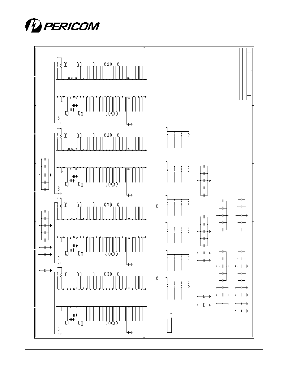
C-6
04/18/00
12345678901234567890123456789012123456789012345678901234567890121234567890123456789012345678901212345678901234567890123456789012123456
12345678901234567890123456789012123456789012345678901234567890121234567890123456789012345678901212345678901234567890123456789012123456
Appendix C
PI7C7100
3-Port PCI Bridge
ADVANCE INFORMATION
A
A
B
B
C
C
D
D
E
E
4
4
3
3
2
2
1
1
PI7C7100
1.3
Three Port PCI Bridge Evaluation Board
C
45
Friday, March 17, 2000
2380 Bering Dr., San Jose,
C
A
Secondary 2 P
C
I
B
u
s
Title
Size
Document Number
Rev
Date:
Sheet
of
AD[31:0]
C/BE[3:0]
AD31
AD30
AD29
AD28
AD27
AD26
AD25
AD24
C/BE3
AD23
AD22
AD21
AD20
AD19
AD18
AD17
AD16
C/BE2
SERR_L
C/BE1
AD15
AD14
AD13
AD12
AD11
AD10
AD9
AD8
C/BE0
AD7
AD6
AD5
AD4
AD3
AD2
AD1
AD0
M66EN
TCK0
TRST0_L
TMS
0
TDI0
AD31
AD30
AD29
AD28
AD27
AD26
AD25
AD24
C/BE3
AD23
AD22
AD21
AD20
AD19
AD18
AD17
AD16
C/BE2
SERR_L
C/BE1
AD15
AD14
AD13
AD12
AD11
AD10
AD9
AD8
C/BE0
AD7
AD6
AD5
AD4
AD3
AD2
AD1
AD0
M66EN
TCK1
TRST1_L
TMS
1
TDI1
AD31
AD30
AD29
AD28
AD27
AD26
AD25
AD24
C/BE3
AD23
AD22
AD21
AD20
AD19
AD18
AD17
AD16
C/BE2
SERR_L
C/BE1
AD15
AD14
AD13
AD12
AD11
AD10
AD9
AD8
C/BE0
AD7
AD6
AD5
AD4
AD3
AD2
AD1
AD0
M66EN
TCK2
TRST2_L
TMS
2
TDI2
SBO2_
L
SBO1_
L
SBO0_
L
SBO0_
L
SDONE0
SBO1_
L
SDONE1
SBO2_
L
SDONE2
SBO3_
L
SDONE0
SDONE2
SDONE1
SDONE3
REQ64#2
ACK64#2
ACK64#0
REQ64#0
ACK64#1
REQ64#1
ACK64#0
ACK64#1
REQ64#0
REQ64#1
ACK64#2
REQ64#2
REQ64#3
ACK64#3
TRDY_L
FRAME_L
IRDY_L
DEVSEL_L
PERR_L
SERR_L
LOCK_L
STOP_
L
AD31
AD30
AD29
AD28
AD27
AD26
AD25
AD24
C/BE3
AD23
AD22
AD21
AD20
AD19
AD18
AD17
AD16
C/BE2
SERR_L
C/BE1
AD15
AD14
AD13
AD12
AD11
AD10
AD9
AD8
C/BE0
AD7
AD6
AD5
AD4
AD3
AD2
AD1
AD0
M66EN
TCK3
TRST3_L
TMS
3
TDI3
SBO3_
L
SDONE3
REQ64#3
ACK64#3
M66EN
+3.3V
+3.3V
+12V
-12V
+3.3V
+5V
+5V
+3.3V
+12
V
-12V
+5V
+3.3V
+12
V
-12V
+5V
+3.3V
+12V
-12V
+3.3V
+3.3V
+3.3V
+3.3V
+3.3V
+3.3V
+3.3V
+3.3V
+5V
+5V
+5V
+3.3V
+5V
+3.3V
C255
0.01uF
C253
0.01uF
C256
0.01uF
C254
0.01uF
R114
5.1K
1
2
R113
5.1K
1
2
C259
0.01uF
C260
0.01uF
C266
0.01uF
C267
0.01uF
C268
0.01uF
C269
0.01uF
C270
0.01uF
C271
0.01uF
C272
0.01uF
C275
0.01uF
C276
0.01uF
C277
0.01uF
C291
0.1uF
C294
0.1uF
C298
0.1uF
C290
0.01uF
C292
0.1uF
C289
0.01uF
C299
0.1uF
C300
0.1uF
C295
0.1uF
C293
0.1uF
C316
0.01uF
C319
0.01uF
C323
0.01uF
C315
0.01uF
C317
0.01uF
C314
0.01uF
C324
0.01uF
+
C311
10uF
C325
0.01uF
C320
0.01uF
C318
0.01uF
C236
0.1uF
C239
0.1uF
C243
0.1uF
C235
0.01uF
C237
0.1uF
C234
0.01uF
+
C232
10uF
C244
0.1uF
C245
0.1uF
C240
0.1uF
C238
0.1uF
R79
5.1K
1
2
R80
5.1K
1
2
R81
5.1K
1
2
R76
5.1K
1
2
R77
5.1K
1
2
R78
5.1K
1
2
R84
5.1K
1
2
R87
5.1K
1
2
R83
5.1K
1
2
R86
5.1K
1
2
R82
5.1K
1
2
R85
5.1K
1
2
R112
5.1K
1
2
R111
5.1K
1
2
R116
5.1K
1
2
R115
5.1K
1
2
U14
PCISLOT
TRST#
A1
+12V
A2
TMS
A3
TDI
A4
+5V
A5
INTA#
A6
INTC#
A7
+5V
A8
NC
A9
+5V
A10
NC
A11
GND
A12
GND
A13
NC
A14
RST#
A15
+5V
A16
GNT#
A17
GND
A18
NC
A19
AD30
A20
+3.3V
A21
AD28
A22
AD26
A23
GND
A24
AD24
A25
IDSEL
A26
+3.3V
A27
AD22
A28
AD20
A29
GND
A30
AD18
A31
AD16
A32
+3.3V
A33
FRAME#
A34
GND
A35
TRDY#
A36
GND
A37
STOP#
A38
+3.3V
A39
SDONE
A40
SBO#
A41
GND
A42
PAR
A43
AD15
A44
+3.3V
A45
AD13
A46
AD11
A47
GND
A48
AD09
A49
NC
A50
NC
A51
C/BE0#
A52
+3.3V
A53
AD06
A54
AD04
A55
GND
A56
AD02
A57
AD00
A58
+5V
A59
REQ64#
A60
+5V
A61
+5V
A62
-12V
B1
TCK
B2
GND
B3
TDO
B4
+5V
B5
+5V
B6
INTB#
B7
INTD#
B8
PRSNT1#
B9
NC
B10
PRSNT2#
B11
GND
B12
GND
B13
NC
B14
GND
B15
CLK
B16
GND
B17
REQ#
B18
+5V
B19
AD31
B20
AD29
B21
GND
B22
AD27
B23
AD25
B24
+3.3V
B25
C/BE3#
B26
AD23
B27
GND
B28
AD21
B29
AD19
B30
+3.3V
B31
AD17
B32
C/BE2#
B33
GND
B34
IRDY#
B35
+3.3V
B36
DEVSEL#
B37
GND
B38
LOCK#
B39
PERR#
B40
+3.3V
B41
SERR#
B42
+3.3V
B43
C/BE1#
B44
AD14
B45
GND
B46
AD12
B47
AD10
B48
M66EN
B49
NC
B50
NC
B51
AD08
B52
AD07
B53
+3.3V
B54
AD05
B55
AD03
B56
GND
B57
AD01
B58
+5V
B59
ACK64#
B60
+5V
B61
+5V
B62
U13
PCISLOT
TRST#
A1
+12V
A2
TMS
A3
TDI
A4
+5V
A5
INTA#
A6
INTC#
A7
+5V
A8
NC
A9
+5V
A10
NC
A11
GND
A12
GND
A13
NC
A14
RST#
A15
+5V
A16
GNT#
A17
GND
A18
NC
A19
AD30
A20
+3.3V
A21
AD28
A22
AD26
A23
GND
A24
AD24
A25
IDSEL
A26
+3.3V
A27
AD22
A28
AD20
A29
GND
A30
AD18
A31
AD16
A32
+3.3V
A33
FRAME#
A34
GND
A35
TRDY#
A36
GND
A37
STOP#
A38
+3.3V
A39
SDONE
A40
SBO#
A41
GND
A42
PAR
A43
AD15
A44
+3.3V
A45
AD13
A46
AD11
A47
GND
A48
AD09
A49
NC
A50
NC
A51
C/BE0#
A52
+3.3V
A53
AD06
A54
AD04
A55
GND
A56
AD02
A57
AD00
A58
+5V
A59
REQ64#
A60
+5V
A61
+5V
A62
-12V
B1
TCK
B2
GND
B3
TDO
B4
+5V
B5
+5V
B6
INTB#
B7
INTD#
B8
PRSNT1#
B9
NC
B10
PRSNT2#
B11
GND
B12
GND
B13
NC
B14
GND
B15
CLK
B16
GND
B17
REQ#
B18
+5V
B19
AD31
B20
AD29
B21
GND
B22
AD27
B23
AD25
B24
+3.3V
B25
C/BE3#
B26
AD23
B27
GND
B28
AD21
B29
AD19
B30
+3.3V
B31
AD17
B32
C/BE2#
B33
GND
B34
IRDY#
B35
+3.3V
B36
DEVSEL#
B37
GND
B38
LOCK#
B39
PERR#
B40
+3.3V
B41
SERR#
B42
+3.3V
B43
C/BE1#
B44
AD14
B45
GND
B46
AD12
B47
AD10
B48
M66EN
B49
NC
B50
NC
B51
AD08
B52
AD07
B53
+3.3V
B54
AD05
B55
AD03
B56
GND
B57
AD01
B58
+5V
B59
ACK64#
B60
+5V
B61
+5V
B62
U15
PCISLOT
TRST#
A1
+12V
A2
TMS
A3
TDI
A4
+5V
A5
INTA#
A6
INTC#
A7
+5V
A8
NC
A9
+5V
A10
NC
A11
GND
A12
GND
A13
NC
A14
RST#
A15
+5V
A16
GNT#
A17
GND
A18
NC
A19
AD30
A20
+3.3V
A21
AD28
A22
AD26
A23
GND
A24
AD24
A25
IDSEL
A26
+3.3V
A27
AD22
A28
AD20
A29
GND
A30
AD18
A31
AD16
A32
+3.3V
A33
FRAME#
A34
GND
A35
TRDY#
A36
GND
A37
STOP#
A38
+3.3V
A39
SDONE
A40
SBO#
A41
GND
A42
PAR
A43
AD15
A44
+3.3V
A45
AD13
A46
AD11
A47
GND
A48
AD09
A49
NC
A50
NC
A51
C/BE0#
A52
+3.3V
A53
AD06
A54
AD04
A55
GND
A56
AD02
A57
AD00
A58
+5V
A59
REQ64#
A60
+5V
A61
+5V
A62
-12V
B1
TCK
B2
GND
B3
TDO
B4
+5V
B5
+5V
B6
INTB#
B7
INTD#
B8
PRSNT1#
B9
NC
B10
PRSNT2#
B11
GND
B12
GND
B13
NC
B14
GND
B15
CLK
B16
GND
B17
REQ#
B18
+5V
B19
AD31
B20
AD29
B21
GND
B22
AD27
B23
AD25
B24
+3.3V
B25
C/BE3#
B26
AD23
B27
GND
B28
AD21
B29
AD19
B30
+3.3V
B31
AD17
B32
C/BE2#
B33
GND
B34
IRDY#
B35
+3.3V
B36
DEVSEL#
B37
GND
B38
LOCK#
B39
PERR#
B40
+3.3V
B41
SERR#
B42
+3.3V
B43
C/BE1#
B44
AD14
B45
GND
B46
AD12
B47
AD10
B48
M66EN
B49
NC
B50
NC
B51
AD08
B52
AD07
B53
+3.3V
B54
AD05
B55
AD03
B56
GND
B57
AD01
B58
+5V
B59
ACK64#
B60
+5V
B61
+5V
B62
C330
0.01uF
C331
0.01uF
R75
5.1K
1
2
R89
5.1K
1
2
R90
5.1K
1
2
R88
5.1K
1
2
U12
PCISLOT
TRST#
A1
+12V
A2
TMS
A3
TDI
A4
+5V
A5
INTA#
A6
INTC#
A7
+5V
A8
NC
A9
+5V
A10
NC
A11
GND
A12
GND
A13
NC
A14
RST#
A15
+5V
A16
GNT#
A17
GND
A18
NC
A19
AD30
A20
+3.3V
A21
AD28
A22
AD26
A23
GND
A24
AD24
A25
IDSEL
A26
+3.3V
A27
AD22
A28
AD20
A29
GND
A30
AD18
A31
AD16
A32
+3.3V
A33
FRAME#
A34
GND
A35
TRDY#
A36
GND
A37
STOP#
A38
+3.3V
A39
SDONE
A40
SBO#
A41
GND
A42
PAR
A43
AD15
A44
+3.3V
A45
AD13
A46
AD11
A47
GND
A48
AD09
A49
NC
A50
NC
A51
C/BE0#
A52
+3.3V
A53
AD06
A54
AD04
A55
GND
A56
AD02
A57
AD00
A58
+5V
A59
REQ64#
A60
+5V
A61
+5V
A62
-12V
B1
TCK
B2
GND
B3
TDO
B4
+5V
B5
+5V
B6
INTB#
B7
INTD#
B8
PRSNT1#
B9
NC
B10
PRSNT2#
B11
GND
B12
GND
B13
NC
B14
GND
B15
CLK
B16
GND
B17
REQ#
B18
+5V
B19
AD31
B20
AD29
B21
GND
B22
AD27
B23
AD25
B24
+3.3V
B25
C/BE3#
B26
AD23
B27
GND
B28
AD21
B29
AD19
B30
+3.3V
B31
AD17
B32
C/BE2#
B33
GND
B34
IRDY#
B35
+3.3V
B36
DEVSEL#
B37
GND
B38
LOCK#
B39
PERR#
B40
+3.3V
B41
SERR#
B42
+3.3V
B43
C/BE1#
B44
AD14
B45
GND
B46
AD12
B47
AD10
B48
M66EN
B49
NC
B50
NC
B51
AD08
B52
AD07
B53
+3.3V
B54
AD05
B55
AD03
B56
GND
B57
AD01
B58
+5V
B59
ACK64#
B60
+5V
B61
+5V
B62
C78
0.1uF
C79
0.1uF
C80
0.01uF
C81
0.01uF
C321
0.01uF
C257
0.01uF
C252
0.01uF
C258
0.01uF
+
C229
10uF
+
C263
10uF
+
C287
10uF
+
C284
10uF
C82
0.1uF
C83
0.1uF
C84
0.01uF
C85
0.01uF
R103
5.1K
1
2
R97
5.1K
1
2
R102
5.1K
1
2
R92
5.1K
1
2
R100
5.1K
1
2
R107
5.1K
1
2
R104
5.1K
1
2
R96
5.1K
1
2
R95
5.1K
1
2
R99
5.1K
1
2
R93
5.1K
1
2
R108
5.1K
1
2
R110
5.1K
1
2
R105
5.1K
1
2
R106
5.1K
1
2
R94
5.1K
1
2
R109
5.1K
1
2
R101
5.1K
1
2
IRDY_L
LOCK_L
PERR_L
FRAME_L
TRDY_L
STOP_
L
PAR
DEVSEL_L
IRDY_L
LOCK_L
PERR_L
FRAME_L
TRDY_L
STOP_
L
DEVSEL_L
IRDY_L
LOCK_L
PERR_L
FRAME_L
TRDY_L
STOP_L
PAR
DEVSEL_L
INTA_L
INTC_L
INTB_L
INTD_L
RESET_L
CLK0
IDSEL0_L
INTC_L
INTA_L
INTD_L
INTB_L
INTA_L
INTC_L
INTB_L
INTD_L
CLK1
CLK2
RESET_L
RESET_L
IDSEL1_L
IDSEL2_L
PAR
AD[31:0]
C/BE[3:0]
GNT0_L
GNT1_L
GNT2_L
REQ0_L
REQ1_L
REQ2_L
SERR_L
SERR_L
SERR_L
IRDY_L
LOCK_L
PERR_L
FRAME_L
TRDY_L
STOP_
L
PAR
DEVSEL_L
INTB_L
INTC_L
INTD_L
INTA_L
CLK3
RESET_L
IDSEL3_L
GNT3_L
REQ3_L
SERR_L
M66EN
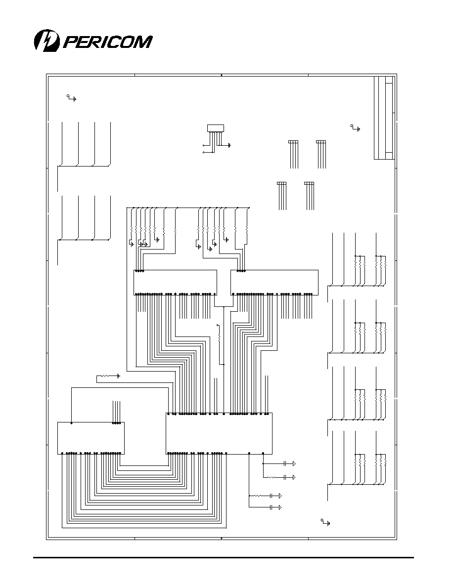
123456789012345678901234567890121234567890123456789012345678901212345678901234567890123456789012123456789012345678901234567890121234567
123456789012345678901234567890121234567890123456789012345678901212345678901234567890123456789012123456789012345678901234567890121234567
C-7
04/18/00
Appendix C
PI7C7100
3-Port PCI Bridge
ADVANCE INFORMATION
A
A
B
B
C
C
D
D
E
E
4
4
3
3
2
2
1
1
Note: Those AGNDs are only connected to a
small GND plane on the top signal layer
PI7C7100
1.3
Three Port PCI Bridge Evaluation Board
C
55
Friday, March 17, 2000
2380 Bering Dr., San Jose,
C
A
Top Vi
e
w
Title
Size
Document Number
Rev
Date:
Sheet
of
Edge
PCIEDGE
IRDY_L
LOCK_L
PERR_L
FRAME_L
TRDY_L
STOP_
L
PAR
DVSEL_L
INTB_L
INTD_L
RESET_L
INTA_L
INTC_L
CLK
REQ_L
GNT_L
M66EN
TCK
TDO
TDI
TM
S
TRST_L
IDSEL_L
SERR_L
AD[31:0]
C/BE[3:0]
S2_INTERFACE
PCIBUS2
IRDY_L
LOCK_L
PERR_L
FRAME_L
TRDY_L
STOP_
L
PAR
DEVSEL_L
REQ0_L
GNT0_L
SERR_L
REQ1_L
GNT1_L
REQ2_L
GNT2_L
REQ3_L
GNT3_L
M66EN
INTA_L
INTC_L
INTB_L
INTD_L
RESET_L
CLK0
IDSEL0_L
CLK1
CLK2
CLK3
IDSEL1_L
IDSEL2_L
IDSEL3_L
AD[31:0]
C/BE[3:0]
S1_INTERFACE
PCIBUS
IRDY_L
LOCK_L
PERR_L
FRAME_L
TRDY_L
STOP_
L
PAR
DEVSEL_L
REQ0_L
GNT0_L
SERR_L
REQ1_L
GNT1_L
REQ2_L
GNT2_L
REQ3_L
GNT3_L
M66EN
INTA_L
INTC_L
INTB_L
INTD_L
RESET_L
CLK0
IDSEL0_L
CLK1
CLK2
CLK3
IDSEL1_L
IDSEL2_L
IDSEL3_L
AD[31:0]
C/BE[3:0]
CHIP
PCICHIP
S2_PAR
S1_FRAMEN
S2_IRDYN
S1_AD[31:0]
P_CBE[3:0]
S2_LOCKN
S1_IRDYN
P_AD[31:0]
S1_LOCKN
S2_PERRN
S2_STOPN
S1_RESETN
S2_DEVSELN
S1_TRDYN
S1_STOPN
S2_CBE[3:0]
S2_RESETN
S2_FRAMEN
S1_DEVSELN
S2_AD[31:0]
S2_TRDYN
S1_PAR
S1_PERRN
S1_CBE[3:0]
S2_SERRN
S2_REQN[7:0]
S2_GNTN[7:0]
S1_REQN[7:0]
S1_SERRN
P_IDSEL
TCK
TDO
TDI
TM
S
P_DEVSELN
P_FRAMEN
P_GNTN
P_IRDYN
P_LOCKN
P_PAR
P_PERRN
P_REQN
P_RESETN
P_SERRN
P_STOPN
P_TRDYN
PLL_CAP2
PLL_CAP1
PLL_SCLK
P_M66EN
S_M66EN
TRST_L
SCLKOUT[15:0]
PLL_PCLK
S1_GNTN[7:0]
INTD_L
INTC_L
INTB_L
INTA_L
INTA_L
INTB_L
INTC_L
INTD_L
INTB_L
INTC_L
INTD_L
INTA_L
S2_IRDY_L
P_C/BE[3:0]
S2_LOCK_L
S2_PERR_L
S2_FRAME_L
S1_PAR_L
S1_PAR_L
P_DEVSEL_L
P_GNT_L
P_LOCK_L
P_PERR_L
S2_STOP
_L
S1_DEVSEL_
L
S2_GNTN[7:0]
P_IRDY_L
P_PERR_L
P_RESET_L
TRST_L
S2_LOCK_L
S2_C/BE[3:0]
S1_PERR_L
TDI
P_STOP_
L
P_TRDY_L
PLL_CAP2
S2_DEVSEL_L
S2_RESET_L
S1_C/BE[3:0]
P_IDSEL_L
S2_IRDY_L
P_AD[31:0]
P_AD[31:0]
S2_PERR_L
S2_STOP
_L
S1_RESET_
L
S1_STOP
_
L
S1_C/BE[3:0]
S1_GNTN[7:0]
P_SERR_L
P_M66EN
S1_FRAME_L
TM
S
P_PAR_L
S2_C/BE[3:0]
S2_RESET_L
S2_AD[31:0]
S1_PERR_L
S2_DEVSEL_
L
S1_STOP
_
L
TCK
P_FRAME_L
P_RESET_L
S_CLK
S1_SERR_L
S2_TRDY_L
S2_SERR_L
P_DEVSEL_L
P_SERR_L
S1_FRAME_L
P_C/BE[3:0]
S1_LOCK_L
S2_REQN[7:0]
TMS
P_GNT_L
PLL_CAP1
S2_PAR_L
P_IRDY_L
P_STOP_
L
S2_FRAME_L
S1_SERR_L
P_IDSEL_L
TCK
TDI
S_M66EN
S2_PAR_L
S2_TRDY_L
S2_SERR_L
TDO
P_LOCK_L
S1_LOCK_L
TDO
P_FRAME_L
P_PAR_L
P_REQ_L
P_TRDY_L
P_M66EN
TRST_L
S1_RESET_
L
S1_DEVSEL_
L
P_REQ_L
P_CLK
S1_REQN[7:0]
S1_TRDY_L
S1_IRDY_L
S1_IRDY_L
S1_TRDY_L
S1_IDSEL0_L
S1_IDSEL1_L
S1_IDSEL2_L
S1_IDSEL3_L
S2_AD[31:0]
S2_IDSEL0_L
S2_AD20
S2_IDSEL1_L
S2_AD21
S2_IDSEL2_L
S2_AD22
S2_IDSEL3_L
S2_AD23
S2_IDSEL0_L
S2_IDSEL1_L
S2_IDSEL2_L
S2_IDSEL3_L
S1_IDSEL3_L
S1_AD23
S1_IDSEL1_L
S1_AD21
S1_IDSEL0_L
S1_AD20
S1_IDSEL2_L
S1_AD22
SCLKOUT0/4
SCLKOUT6
SCLKOUT2/6
SCLKOUT3/7
SCLKOUT1/5
SCLKOUT[15:0]
SCLKOUT8/12
SCLKOUT9/13
SCLKOUT11/15
SCLKOUT10/14
SCLKOUT13
SCLKOUT14
S1_GNTN[7:0]
S
1_REQN[7:0]
S2_GNTN[7:0]
S
2_REQN[7:0]
S1_GNTN5
S1_REQN5
S2_GNTN5
S2_REQN5
S1_REQN3/7
S1_REQN7
S1_REQN1/5
S1_GNTN3/7
S1_GNTN7
S1_GNTN1/5
S1_GNTN2/6
S1_GNTN6
S1_REQN2/6
S1_REQN6
S2_REQN1/5
S2_GNTN1/5
S2_REQN2/6
S2_REQN6
S2_GNTN3/7
S2_GNTN7
S2_GNTN2/6
S2_GNTN6
S2_REQN3/7
S2_REQN7
S1_GNTN1/5
S1_GNTN2/6
S1_GNTN3/7
S1_GNTN0/4
S1_REQN0/4
S1_REQN2/6
S1_REQN1/5
S1_REQN3/7
S2_REQN1/5
S2_GNTN3/7
S2_GNTN2/6
S2_REQN0/4
S2_REQN2/6
S2_REQN3/7
S2_GNTN0/4
S2_GNTN1/5
SCLKOUT12
SCLKOUT11
SCLKOUT10
SCLKOUT9
SCLKOUT8
SCLKOUT5
SCLKOUT0
S1_GNTN4
S1_GNTN0/4
S1_GNTN3
S1_GNTN2
S1_GNTN1
S1_GNTN0
S1_REQN0
S1_REQN0/4
S1_REQN4
S1_REQN2
S1_REQN1
S1_REQN3
S2_GNTN0
S2_GNTN0/4
S2_GNTN4
S2_GNTN2
S2_GNTN1
S2_GNTN3
S2_REQN0
S2_REQN0/4
S2_REQN4
S2_REQN2
S2_REQN1
S2_REQN3
SCLKOUT7
SCLKOUT15
S1_AD[31:0]
S1_AD[31:0]
S2_GNTN3/7
S2_GNTN2/6
S2_GNTN0/4
S2_GNTN1/5
S2_REQN1/5
S2_REQN0/4
S2_REQN2/6
S2_REQN3/7
S1_REQN0/4
S1_REQN2/6
S1_REQN1/5
S1_REQN3/7
S1_GNTN1/5
S1_GNTN2/6
S1_GNTN3/7
S1_GNTN0/4
SCLKOUT4
SCLKOUT2
SCLKOUT1
SCLKOUT3
+5V
+3.3V
+3.3V
C350
100
p
C351
100p
R148
4.7k
R150
4.7k
U20
Test Point
T
U19
Test Point
T
U17
Test Point
T
C352
47p
C349
47p
R174
22
1
2
R164
0
1
2
R163
0
1
2
R162
0
1
2
R161
0
1
2
P1
HEADER 6
1
2
3
4
5
6
R199
5.1K
1
2
R173
22
1
2
R152
22
1
2
R151
22
1
2
R149
22
1
2
R147
22
1
2
R170
22
1
2
R143
22
1
2
R165
0
1
2
R177
0
1
2
R178
0
1
2
R179
0
1
2
R180
0
1
2
R184
0
1
2
R166
0
1
2
R182
0
1
2
R183
0
1
2
R181
0
1
2
R188
0
1
2
R167
0
1
2
R186
0
1
2
R187
0
1
2
R185
0
1
2
R192
0
1
2
R168
0
1
2
R190
0
1
2
R191
0
1
2
R189
0
1
2
R171
22
1
2
R172
22
1
2
R175
22
1
2
R176
22
1
2
U22
1header
T
1
U23
1header
T
1
U24
1header
T
1
U25
1header
T
1
U26
1header
T
1
U27
1header
T
1
U28
1header
T
1
U29
1header
T
1
U30
1header
T
1
U31
1header
T
1
U32
1header
T
1
U33
1header
T
1
U34
1header
T
1
U35
1header
T
1
U36
1header
T
1
U37
1header
T
1
R49
5.1K
1
2
R169
22
1
2
R145
22
1
2
R144
22
1
2
R146
22
1
2

C-8
04/18/00
12345678901234567890123456789012123456789012345678901234567890121234567890123456789012345678901212345678901234567890123456789012123456
12345678901234567890123456789012123456789012345678901234567890121234567890123456789012345678901212345678901234567890123456789012123456
Appendix C
PI7C7100
3-Port PCI Bridge
ADVANCE INFORMATION

D1
09/18/00 Rev 1.1
123456789012345678901234567890121234567890123456789012345678901212345678901234567890123456789012123456789012345678901234567890121234567
123456789012345678901234567890121234567890123456789012345678901212345678901234567890123456789012123456789012345678901234567890121234567
PI7C7100
3-Port PCI Bridge
ADVANCE INFORMATION
PI7C7100
3-Port
PCI Bridge
Appendix D
Representatives
& Distributors

D2
09/18/00 Rev 1.1
12345678901234567890123456789012123456789012345678901234567890121234567890123456789012345678901212345678901234567890123456789012123456
12345678901234567890123456789012123456789012345678901234567890121234567890123456789012345678901212345678901234567890123456789012123456
PI7C7100
3-Port PCI Bridge
ADVANCE INFORMATION
Corporate Headquarters
Pericom Semiconductor Corp.
2380 Bering Drive,
San Jose, CA 95131-USA
1-800 435-2336
408 435-0800
408 435 1100 Fax
nolimits@pericom.com
Northern California, Western USA & British Columbia
Pericom Semiconductor Corp.
2380 Bering Drive,
San Jose, CA 95131-USA
1-800 435-2336
408 435-0800
408 435 1100 Fax
rgorshe@pericom.com
Southern California-USA
Pericom Semiconductor Corp.
3455 Lebon Street, Suite 1536
San Diego, CA 92212-USA
858 558-6975
858 558 6685 Fax
nsoo@pericom.com
North Central & South Central USA
Pericom Semiconductor Corp.
5068 West Plano Parkway, Suite 300
Plano, TX 75093-USA
972 381-4209
972 381 4208
mmorse@pericom.com
Mid Atlantic and South East USA
Pericom Semiconductor Corp
1143-B Executive Circle
Cary, NC 27511-USA
919 460-3177
919 460 3179 Fax
mward@pericom.com
North East and Mid and Eastern Canada
Pericom Semiconductor Corp
Radnor Station Building #2
290 King of Prussia Road, Suite 104
Radnor, PA 19087
610.293.7400
610.293.7410 Fax
gfrancisco@pericom.com
Europe
Pericom Semiconductor Corp.
The Enterprise Center
1-2 Davy Road
Gorse Lane Industrial Center
Clacton On Sea, Essex, UK CO15 4XD
44 1255 479994
44 1255 223676 Fax
johara@pericom.com
China - Peoples Republic of China
Pericom Technology Inc.
481 Gui Ping Road 3F, Building 20
Shanghai, 200233
86 21 6485 0576
86 21 6485 2181 Fax
afock@pericom.com
Hong Kong
Pericom Technology Inc.
8 Wang Hoi Road, Unit 1517
Chevalier Commercial Center
Kowloon Bay, Hong Kong
852 2243 3660
852 2243 3667 Fax
qshuai@pti.com.cn
Taiwan R.O.C.
Pericom Semiconductor Corp.
11F, No. 18, Alley 1, Lane 768, Sec 4 Pa Te Road
Taipei, Taiwan - R.O.C.
886 2 2651 5159
886 2 2653 0041 Fax
mchiang@pericom.com
Singapore
Pericom Semiconductor Corp.
42 Mactaggart Road #04-01 Mactaggart Building
Singapore 368086
65 287 9705
65 287 9706 Fax
tctee@postone.com
Japan
Pericom Semiconductor Corp.
Yamamasa Daiichi Building 5, 2-11-3 Kobuchi
Sagamihara-shi, Kanagawa 229-0004-Japan
81 427 86 7266
81 427 86 7267 Fax
ksato@pericom.com
Pericom Corporate Offices

D3
09/18/00 Rev 1.1
123456789012345678901234567890121234567890123456789012345678901212345678901234567890123456789012123456789012345678901234567890121234567
123456789012345678901234567890121234567890123456789012345678901212345678901234567890123456789012123456789012345678901234567890121234567
PI7C7100
3-Port PCI Bridge
ADVANCE INFORMATION
North America Distributors
Company Name
Street Address
City
State
Zip Code
Country
Telephone
Fax Number
All American ................................... 4950 Corporate Drive, Suite 115D ............................................. Huntsville .................. AL ............. 35805 ............. USA ....... 800 382-5303 ....... 256-837-7733
Future ............................................. 6767 Old Madison Pike, Suite 400A ........................................... Huntsville .................. AL ............. 35806 ............. USA ....... 256-971-2010 ...... 256-922-0004
Nu Horizons ................................... 4825 University Square, Suite 8 ................................................ Huntsville .................. AL ............. 35816 ............. USA ....... 256-722-9330 ...... 256-722-9348
Pioneer-Standard Electronics .......... 4910 University Square, Suite 7 ................................................ Huntsville .................. AL ............. 35816 ............. USA ....... 256 837-9300 ....... 256-837-9385
FAI ................................................. 11219 Financial Centre Parkway, Financial Park Place, Ste 311 .. Little Rock .................. AR ............ 72211 ............. USA ....... 501-219-1707 ...... 501-219-1747
All American ................................... 4636 East University Drive, Suite 155 ........................................ Phoenix ...................... AZ ............ 85034 ............. USA ....... 480-966-0006 ...... 480-966-0007
Bell Microproducts .......................... 4926 East McDowell Road, Suite 102 ........................................ Phoenix ...................... AZ ............ 85008 ............. USA ....... 602-267-9551 ...... 602-267-8911
FAI ................................................. 4636 East University Drive, Suite 145 ........................................ Phoenix ...................... AZ ............ 85034 ............. USA ....... 480-731-4661 ...... 480-731-9866
Future ............................................. 4636 East University Drive, Suite 245 ........................................ Phoenix ...................... AZ ............ 85034 ............. USA ....... 602-968-7140 ...... 602-968-0334
Nu Horizons ................................... 1295 West Washington Street, Suite 212 ................................... Tempe ....................... AZ ............ 85281 ............. USA ....... 602 685-9000 ....... 602-685-9004
Pioneer-Standard Electronics .......... 4908 East McDowell Road, Suite 103 ........................................ Phoenix ...................... AZ ............ 85008 ............. USA ....... 602-231-6400 ...... 602-321-8877
Aegis Electronics Group .................. 1015 Chestnut Avenue, Suite G2 ............................................... Carlsbad ................... CA ............ 92208 ............. USA ....... 760 729-2026 .......
All American ................................... 10805 Holder Street, Suite 100 .................................................. Cypress ..................... CA ............ 90630 ............. USA ....... 714 229-8600 ....... 714-229-8603
All American ................................... 14192 Chambers Road ............................................................. Tustin ........................ CA ............ 92680 ............. USA ....... 714 573-5000 ....... 714-573-5047
All American ................................... 1545 East Acequia, Suite A ....................................................... Visalia ....................... CA ............ 93292 ............. USA ....... 209 734-8861 .......
All American ................................... 230 Devcon Drive ..................................................................... San Jose ................... CA ............ 95112 ............. USA ....... 800-222-6001 ...... 408-437-8970
All American ................................... 26010 Mureau Road, Suite 120 ................................................. Calabasas ................. CA ............ 91302 ............. USA ....... 818 878-0555 ....... 818-878-0533
All American ................................... 6390 Greenwich Drive, Suite 170 ............................................... San Diego ................. CA ............ 92122 ............. USA ....... 800-382-3441 ...... 619-658-0201
Bell Microproducts .......................... 1921 Ringwood Avenue ............................................................. San Jose ................... CA ............ 95131-1721 .... USA ....... 408 451-9400 ....... 408-467-2734
Bell Microproducts .......................... 30 Fairbanks, Suite 114 ............................................................ Irvine ......................... CA ............ 92618 ............. USA ....... 949 470-2900 ....... 949-470-2929
Bell Microproducts .......................... 5090 Shoreham Place, Suite 206 ............................................... San Diego ................. CA ............ 92121 ............. USA ....... 858 597-3010 ....... 858-597-3015
Bell Microproducts .......................... 29800 West Agoura Road, Suite 150 ......................................... Agoura Hills .............. CA ............ 91301 ............. USA ....... 818 865-0266 ....... 818-865-0215
FAI ................................................. 354 Bel Marin Keys Blvd., Suite D ............................................. Novato ....................... CA ............ 94949 ............. USA ....... 415 883-9446 ....... 415-883-8336
FAI ................................................. 525 South Douglas Street ......................................................... El Segundo ................ CA ............ 90245 ............. USA ....... 310 727-1754 ....... 310-727-1796
FAI ................................................. 2220 O'Toole Ave. .................................................................... San Jose ................... CA ............ 95131 ............. USA ....... 408 434-0369 ....... 408-433-9599
FAI ................................................. 6256 Greenwich Drive, Suite 200 .............................................. San Diego ................. CA ............ 92122 ............. USA ....... 858-623-5859 ...... 858-623-5860
FAI ................................................. 25B Technology Drive, Suite 200 .............................................. Irvine ......................... CA ............ 92618 ............. USA ....... 949-753-4778 ...... 949-753-4778
FAI ................................................. 26570 Agoura Road ................................................................. Calabasas ................. CA ............ 91302 ............. USA ....... 818 871-1700 ....... 818-871-1726
FAI ................................................. 3009 Douglas Blvd., Suite 215 .................................................. Roseville ................... CA ............ 95661 ............. USA ....... 916-782-7882 ...... 916-782-9388
FAI ................................................. 1370 Valley Vista Drive, Suite 265 ............................................. Diamond Bar ............. CA ............ 91765 ............. USA ....... 909 612-0667 ....... 909-612-0167
FAI ................................................. 2121 41st Avenue ..................................................................... Capitola ..................... CA ............ 95010 ............. USA ....... 831 465-7373 ....... 831-465-7299
Future ............................................. 2220 O'Toole Ave. .................................................................... San Jose ................... CA ............ 95131 ............. USA ....... 408 434-1122 ....... 408-433-0822
Future ............................................. 26570 Agoura Road ................................................................. Calabasas ................. CA ............ 91302 ............. USA ....... 818 871-1740 ....... 818-871-1764
Future ............................................. 25B Technology Drive, Suite 200 .............................................. Irvine ......................... CA ............ 92618 ............. USA ....... 949-453-1515 ...... 949-453-1226
Future ............................................. 27489 West Agoura Road, Suite 300 ......................................... Agoura Hills .............. CA ............ 91301 ............. USA ....... 818 865-0040 .......
Future ............................................. 3009 Douglas Blvd., Suite 210 .................................................. Roseville ................... CA ............ 95661 ............. USA ....... 916 783-7877 ....... 916-783-7988
Future ............................................. 5990 Stoneridge Drive .............................................................. Pleasanton ................. CA ............ 94588 ............. USA ....... 925 225-0294 ....... 925 225-9745
Future ............................................. 6256 Greenwich Drive, Suite 200 .............................................. San Diego ................. CA ............ 92122 ............. USA ....... 858-625-2800 ...... 858-625-2810
Nu Horizons ................................... 1220 Melody Lane, Suite 110 .................................................... Roseville ................... CA ............ 95678 ............. USA ....... 916 783-5500 ....... 916-783-3066
Nu Horizons ................................... 13900 Alton Parkway, Suite 123 ................................................. Irvine ......................... CA ............ 92718 ............. USA ....... 949 470-1011 ....... 949-470-1104
Nu Horizons ................................... 2070 Ringwood Avenue ............................................................ San Jose ................... CA ............ 95131 ............. USA ....... 408 434-0800 ....... 408-434-0935
Nu Horizons ................................... 4360 View Ridge Avenue, Suite B ............................................. San Diego ................. CA ............ 92123 ............. USA ....... 619 576-0088 ....... 619-576-0990
Nu Horizons ................................... 850 Hampshire Road, Suite R .................................................. Thousand Oaks .......... CA ............ 91361 ............. USA ....... 805 370-1515 ....... 805-370-1525
Pioneer-Standard Electronics .......... 217 Technology Drive, Suite 110 ............................................... Irvine ......................... CA ............ 92618 ............. USA ....... 949-753-5090 ...... 949-753-5074
Pioneer-Standard Electronics .......... 333 River Oaks Pkwy. ............................................................... San Jose ................... CA ............ 95134 ............. USA ....... 408 954-9100 .......
Pioneer-Standard Electronics .......... 5126 Clareton Drive, Suite 100 ................................................. Agoura Hills .............. CA ............ 91301 ............. USA ....... 818 865-5800 ....... 818-865-5814
Pioneer-Standard Electronics .......... 9449 Balboa Ave., Suite 114 ...................................................... San Diego ................. CA ............ 92123 ............. USA ....... 858-514-7700 ...... 858-514-7799
Pioneer-Standard Electronics .......... 431 Dixon Landing Road .......................................................... Milpitas ..................... CA ............ 95035 ............. USA ....... 408 586-5600 ....... 408-586-5785
All American ................................... 7577 West 103rd Avenue, Suite 204 .......................................... Westminster .............. CO ............ 80021 ............. USA ....... 303-222-0100 ...... 303-222-0110
All American ................................... 4090 Youngfield Street ............................................................. Wheat Ridge ............. CO ............ 80033 ............. USA ....... 303 422-1701 .......
Bell Microproducts .......................... 4600 South Ulster Street, Suite 240 .......................................... Denver ....................... CO ............ 80237 ............. USA ....... 303-846-3065 ...... 303-846-3064
Future ............................................. 1819 Denver West Drive, Bldg. 26, Suite 350 ............................ Golden ....................... CO ............ 80401 ............. USA ....... 303 277-0023 ....... 303-277-0722
Pioneer-Standard Electronics .......... 5600 Greenwood Plaza Blvd. Suite 200 ..................................... Englewood ................. CO ............ 80111 ............. USA ....... 303 773-8090 ....... 303-773-8194
All American ................................... 100 Mill Plain Road, Suite 360 .................................................. Danbury ..................... CT ............ 06811 ............. USA ....... 203 791-3818 .......
All American ................................... 83 Papermill Road ................................................................... Woodbury .................. CT ............ 6798 ............... USA ....... 203-266-0486 ...... same
Future ............................................. 700 West Johnson Avenue, Westgate Office Center .................. Cheshire ................... CT ............ 06410 ............. USA ....... 203 250-0083 ....... 203-250-0081
Pioneer-Standard Electronics .......... Two Trap Falls Road, Suite 100 ............................................... Shelton ...................... CT ............ 06484 ............. USA ....... 203-929-5600 ...... 203-929-9791
All American ................................... 600 Fairway Drive, Suite 101 .................................................... Deerfield Beach ......... FL ............. 33441 ............. USA ....... 954 429-2800 ....... 954-429-0391
All American ................................... 528 South North Lake Blvd., Suite 1040 ..................................... Altamonte Springs ..... FL ............. 32701 ............. USA ....... 407 261-1304 ....... 407-261-1330
All American ................................... 14450 46th Street North, Suite 116 ............................................ Clearwater ................. FL ............. 33762 ............. USA ....... 813 532-9800 ....... 813-538-5567
All American ................................... 16115 NW 52nd Avenue ............................................................ Miami ........................ FL ............. 33014 ............. USA ....... 305 621-8282 ....... 305-620-7831
Bell Microproducts .......................... 17431 SW 18th Street ............................................................... Miramar .................... FL ............. 33029 ............. USA ....... 954-450-1850 ...... 954-450-0223
Bell Microproducts .......................... 1110 Douglas Avenue, Suite 1018 ............................................. Altamonte Springs ..... FL ............. 32714 ............. USA ....... 407 682-1199 ....... 407-682-1286
Bell Microproducts .......................... 1761 West Hillsboro Blvd., Suite 208 ......................................... Deerfield Beach ......... FL ............. 33442 ............. USA ....... 954 429-1001 .......
Edge Electronics ............................. 100 Second Avenue South, Suite 200 ......................................... St. Petersburg ........... FL ............. 33701 ............. USA ....... 727-894-3343 ...... 727-823-9030
FAI ................................................. 525 Technology Park, Suites 125/126 ........................................ Lake Mary .................. FL ............. 32746 ............. USA ....... 407 333-3177 ....... 407-333-3277
FAI ................................................. 348 SW Miracle Strip Pkwy., Suite 33 ........................................ Fort Walton Beach ..... FL ............. 32548 ............. USA ....... 850 301-0766 ....... 850-301-0773
FAI ................................................. 2200 Tall Pines Drive, Suite 109 ............................................... Largo ........................ FL ............. 34641 ............. USA ....... 727-530-1665 ...... 727-530-7609
Future ............................................. 1400 East Newport Center Drive, Suite 200 ............................... Deerfield Beach ......... FL ............. 33442 ............. USA ....... 954 428-9494 ....... 954-428-9477
Future ............................................. 237 South Westmonte Drive, Suite 307 ...................................... Altamonte Springs ..... FL ............. 32714 ............. USA ....... 407 444-6302 ....... 407-444-6303
Future ............................................. 2200 Tall Pines Drive, Suite 108 ............................................... Largo ........................ FL ............. 33771 ............. USA ....... 727-530-1222 ...... 727-538-9598
Nu Horizons ................................... 3421 N.W. 55th Street .............................................................. Ft. Lauderdale ............ FL ............. 33309 ............. USA ....... 954 735-2555 ....... 954-735-2880
Nu Horizons ................................... 4500 140th Avenue North, Suites 214/215 .................................. Clearwater ................. FL ............. 33762 ............. USA ....... 727-536-5700 ...... 727-536-7799
Nu Horizons ................................... 600 South North Lake Blvd., Suite 210 ....................................... Altamonte Springs ..... FL ............. 32701 ............. USA ....... 407 831-8008 ....... 407-931-8862
Pioneer-Standard Electronics .......... 337 South North Lake, Suite 1000 .............................................. Alamonte Springs ...... FL ............. 32701 ............. USA ....... 407 834-9090 ....... 407-834-0865
Pioneer-Standard Electronics .......... 674 South Military Trail ............................................................ Deerfield Beech ......... FL ............. 33442 ............. USA ....... 954 428-8877 ....... 954-481-2950

D4
09/18/00 Rev 1.1
12345678901234567890123456789012123456789012345678901234567890121234567890123456789012345678901212345678901234567890123456789012123456
12345678901234567890123456789012123456789012345678901234567890121234567890123456789012345678901212345678901234567890123456789012123456
PI7C7100
3-Port PCI Bridge
ADVANCE INFORMATION
Company Name
Street Address
City
State
Zip Code
Country
Telephone
Fax Number
All American ................................... 6875 Jimmy Carter Blvd., Suite 3100 ......................................... Norcross ................... GA ............ 30071 ............. USA ....... 770 441-7500 ....... 770-441-3660
Bell Microproducts .......................... 1950 Spectrum Circle, Suite 400 ............................................... Marietta ..................... GA ............ 30067 ............. USA ....... 770-980-4922 ...... 770-857-4399
Future ............................................. 44000 River Green Parkway, Suite 220 ...................................... Duluth ....................... GA ............ 30096 ............. USA ....... 770 476-3900 ....... 770-476-8662
Future ............................................. 3150 Hocomb Bridge Rd. Holcolm Place, Suite 130 ................. Norcross ................... GA ............ 30071 ............. USA ....... 770 441-7676 .......
Nu Horizons ................................... 100 Pinnacle Way, Suite 155 ..................................................... Norcross ................... GA ............ 30071 ............. USA ....... 770 416-8666 ....... 770-416-9060
Pioneer-Standard Electronics .......... 4250-C Rivergreen Pkwy. ......................................................... Duluth ....................... GA ............ 30096 ............. USA ....... 770 623-1003 ....... 770-623-0665
FAI ................................................. 12438 West Bridger Street, Suite 110 ....................................... Boise ......................... ID ............. 83713 ............. USA ....... 208 376-8080 ....... 208-376-6186
All American ................................... 1930 North Thoreau Drive, Suite 200 ........................................ Schaumburg .............. IL .............. 60173 ............. USA ....... 847 303-1995 ....... 847-303-1996
Bell Microproducts .......................... 953 Plum Grove Road, Suite B .................................................. Schaumburg .............. IL .............. 60173 ............. USA ....... 847 413-8530 ....... 847-413-8541
FAI ................................................. 3100 West Higgins Road, Suite 115 ......................................... Hoffman Estates ........ IL .............. 60195 ............. USA ....... 847 843-0034 ....... 847-843-1163
Future ............................................. 3100 West Higgins Road, Suite 100 ......................................... Hoffman Estates ........ IL .............. 60195 ............. USA ....... 847 882-1255 ....... 847-490-9290
Nu Horizons ................................... Basswood Office Center, 500 East Remington Road, Suite 104 . Schaumburg .............. IL .............. 60173 ............. USA ....... 847 519-0700 ....... 847-519-7710
Pioneer-Standard Electronics .......... 2171 Executive Drive Suite 200 ................................................. Addison ..................... IL .............. 60101 ............. USA ....... 630 495-9680 ....... 630-495-9831
Future ............................................. 8520 Allison Pointe Blvd., Suite 310 .......................................... Indianapolis ............... IN ............. 46250 ............. USA ....... 317 913-1355 ....... 317-913-1375
Future ............................................. 8425 Woodfield Crossing, Suite 170 ......................................... Indianapolis ............... IN ............. 46240 ............. USA ....... 317 469-0447 ....... 317-49-0448
Pioneer-Standard Electronics .......... 237 Airport N. Office Park ......................................................... Fort Wayne ................ IN ............. 46285 ............. USA ....... 219 489-0283 .......
Pioneer-Standard Electronics .......... 9350 N. Priority Way W. Drive ................................................... Indianapolis ............... IN ............. 46240 ............. USA ....... 317 573-0880 .......
All American ................................... 7201 West 129th Street, Suite 150 ............................................. Overland Park ............ KS ............ 66213 ............. USA ....... 913 851 5900 ....... 913-851-5905
FAI ................................................. 10977 Granada Lane, Suite 210 ................................................ Overland Park ............ KS ............ 66211 ............. USA ....... 913 338-4400 ....... 913-338-3412
Pioneer-Standard Electronics .......... 8500 College Blvd., Suite 128 ................................................... Overland .................... KS ............ 66210 ............. USA ....... 913-338-7164 ...... 913-338-7185
All American ................................... 19-A Crosby Drive ................................................................... Bedford ...................... MA ............ 01730 ............. USA ....... 781-275-8888 ...... 617-275-1982
Bell Microproducts .......................... 2A Gill Street ........................................................................... Woburn ...................... MA ............ 1730 ............... USA ....... 781-933-9010 ...... 781-933-8336
Future ............................................. 41 Main Street ......................................................................... Bolton ........................ MA ............ 01740 ............. USA ....... 978 779-3000 ....... 978-779-3050
Interface Electronics ........................ 124 Grove Street, Suite 300 ...................................................... Franklin ..................... MA ............ 2038 ............... USA ....... 508-553-4200 ...... 508-553-9575
Interface Electronics ........................ 228 South Street ....................................................................... Hopkinton .................. MA ............ 1748 ............... USA ....... 508 435-0100 .......
Nu Horizons ................................... 2 Corporation Way, Suite 240 .................................................... Peabody ..................... MA ............ ,01960 ............ USA ....... 978 532-7666 ....... 978-532-7667
Pioneer-Standard Electronics .......... 299 Callardvale Street .............................................................. Wilmington ................ MA ............ ,01887 ............ USA ....... 978 988-6600 ....... 978-988-6620
All American ................................... 8310 Guilford Road, Suite A ..................................................... Columbia ................... MD ........... 21046 ............. USA ....... 410 309-6262 ....... 410-309-6272
Bell Microproducts .......................... 6925 R. Oakland Mills Road ..................................................... Columbia ................... MD ........... 21045 ............. USA ....... 410 720-5100 ....... 410-381-2172
Future ............................................. 857 Elkridge Landing Road, International Tower ....................... Linthicum ................... MD ........... 21090 ............. USA ....... 410 314-1111 ....... 410-314-1110
Future ............................................. 6716 Alexander Bell Drive, Suite 220 ......................................... Columbia ................... MD ........... 21046 ............. USA ....... 410 290-0600 .......
Nu Horizons ................................... 8965 Guilford Road, Suite 100 .................................................. Columbia ................... MD ........... 21046 ............. USA ....... 310-995-6330 ...... 310-995-6332
Pioneer-Standard Electronics .......... 9100 Gaither Road ................................................................... Gaithersburg ............. MD ........... 20877 ............. USA ....... 301 921-0660 ....... 301-670-6746
All American ................................... 39201 Schoolcraft Road, Suite B-2 ........................................... Livonia ....................... MI ............. 48150 ............. USA ....... 734-464-2202 ...... 734-464-2433
Future ............................................. 39340 Country Club Drive, Suite 100 ......................................... Famingron Hills ........ MI ............. 48331 ............. USA ....... 248 489-1179 ....... 248-489-1030
Future ............................................. 4595 Broadmoor SE., Suite 280 ................................................ Grand Rapids ............ MI ............. 49512 ............. USA ....... 616 534-3510 ....... 616-698-6821
Pioneer-Standard Electronics .......... 44190 Plymouth Oaks Blvd. ....................................................... Plymouth .................... MI ............. 48170 ............. USA ....... 734-416-2157 ...... 734-416-2415
Pioneer-Standard Electronics .......... 4476 Byron Center Road SW .................................................... Grand Rapids ............ MI ............. 49509 ............. USA ....... 616-534-3145 ...... 616-534-3922
All American ................................... 6608 Flying Cloud Drive ........................................................... Eden Prairie .............. MN ........... 55344 ............. USA ....... 612 944-2151 ....... 612-944-9803
Bell Microproducts .......................... Primetech Center 1, 6442 City West Parkway, Suite 200 ............ Eden Prairie .............. MN ........... 55344 ............. USA ....... 612 943-1122 ....... 612-943-1110
Future ............................................. 18882 Lake Drive East .............................................................. Chanhassen .............. MN ........... 55317 ............. USA ....... 612 934-9100 ....... 612-934-6700
Future ............................................. 10025 Valley View Road, Suite 196 ........................................... Eden Prairie .............. MN ........... 55344 ............. USA ....... 612 944-2200 .......
Nu Horizons ................................... 10907 Valley View Road ........................................................... Eden Prairie .............. MN ........... 55344 ............. USA ....... 612 942-9030 ....... 612-942-9144
Pioneer-Standard Electronics .......... 7625 Golden Triangle Drive, Suite G ........................................ Eden Prairie .............. MN ........... 55344 ............. USA ....... 612-944-3794 ...... 612-829-2229
FAI ................................................. 12125 Woodcrest Executive Drive, Suite 208 ............................. St. Louis .................... MO ........... 63141 ............. USA ....... 314-542-9922 ...... 314-542-9655
Future ............................................. 12125 Woodcrest Executive Drive, Suite 206 ............................. St. Louis .................... MO ........... 63141 ............. USA ....... 314-469-6805 ...... 314-469-7226
Pioneer-Standard Electronics .......... 4227 Earth City Expressway ...................................................... Earth City .................. MO ........... 63045 ............. USA ....... 314-209-3000 ...... 314-209-3054
All American ................................... 1121 Situs Court, Suite 370 ...................................................... Raleigh ..................... NC ............ 27606 ............. USA ....... 919 851-6566 ....... 919-851-8734
FAI ................................................. 5225 Capital Blvd., 1 North Commerce Center .......................... Raleigh ..................... NC ............ 27616 ............. USA ....... 919 790-7111 ....... 919-790-9022
FAI ................................................. 2800 Sumner Blvd., Suite 154 .................................................... Raleigh ..................... NC ............ 27616 ............. USA ....... 919 876-0088 ....... 919-876-8597
Future ............................................. 8401 University Executive Parkway, Suite 108 ............................ Charlotte ................... NC ............ 28262 ............. USA ....... 704-548-9503 ...... 704-548-9469
Interface Electronics ........................ 4601 Six Forks Road, Suite 133 ................................................ Raleigh ..................... NC ............ 27609 ............. USA ....... 919-787-8744 ...... 919-787-9192
Nu Horizons ................................... 2920 Highwood Boulevard, Suite 125 ........................................ Raleigh ..................... NC ............ 27604 ............. USA ....... 919 954-0500 ....... 919-954-0545
Pioneer-Standard Electronics .......... 5510 Six Forks Road, Suite 310 ................................................ Raleigh ..................... NC ............ 27609 ............. USA ....... 919-845-5100 ...... 919-845-5055
All American ................................... 8 East Stow Road, Suite 100 ..................................................... Marlton ...................... NJ ............ 8053 ............... USA ....... 609-596-6666 ...... 609-797-1700
Bell Microproducts .......................... 55 U.S. Highway 46 East, Suite 403 .......................................... Pine Brook ................. NJ ............ ,07058 ............ USA ....... 973-244-9668 ...... 973-244-9667
Bell Microproducts .......................... 23 Sebago Street ..................................................................... Clifton ....................... NJ ............ 7013 ............... USA ....... 201 777-4100 .......
FAI ................................................. 2000 Crawford Place, Suite 900 ................................................ Mt. Laurel .................. NJ ............ ,08054 ............ USA ....... 856 787-1000 ....... 856-787-9626
Future ............................................. 12 East Stow Road, Suite 200 ................................................... Marlton ...................... NJ ............ 08053 ............. USA ....... 609 596-4080 .......
Future ............................................. 1259 Route 46 East .................................................................. Parsippany ................. NJ ............ 07054 ............. USA ....... 973 299-0400 ....... 973-299-1377
Interface Electronics ........................ 20000 Horizon Way, Suite 300 .................................................. Mt. Laural .................. NJ ............ 8054 ............... USA ....... 609-439-0750 ...... 609-439-0519
Interface Electronics ........................ 1 Green Tree, Suite 201 ........................................................... Marlton ...................... NJ ............ 8053 ............... USA ....... 609 988-5448 .......
Nu Horizons ................................... 18000 Horizon Way, Suite 200 .................................................. Mt. Laural .................. NJ ............ 08054 ............. USA ....... 609 231-0900 ....... 609-231-9510
Nu Horizons ................................... 39 U.S. Route 46 ...................................................................... Pine Brook ................. NJ ............ 07058 ............. USA ....... 973-882-8300 ...... 973-882-8398
Pioneer-Standard Electronics .......... 271 Route 46W, Suite D206 ...................................................... Fairfield ..................... NJ ............ ,07004 ............ USA ....... 973 227-7760 ....... 973-227-3305
Pioneer-Standard Electronics .......... 14A Madison Road ................................................................... Fairfield ..................... NJ ............ 7004 ............... USA ....... 201 575-3510 .......
FAI ................................................. 5250 Neil Road, Suite 106 ........................................................ Reno ......................... NV ............ 89502 ............. USA ....... 715-826-2500 ...... 715-826-2664
All American ................................... 275B Marcus Blvd. ................................................................... Hauppauge ................ NY ............ 11788 ............. USA ....... 516 434-9000 ....... 516-434-9394
All American ................................... 333 Metro Park ........................................................................ Rochester .................. NY ............ 14623 ............. USA ....... 716 292-6700 ....... 716-292-6755
Bell Microproducts .......................... 1056 West Jericho Turnpike ..................................................... Smithtown .................. NY ............ 11787 ............. USA ....... 516 543-2000 ....... 516-543-2030
Edge Electronics ............................. 2271-7 Fifth Avenue .................................................................. Ronkonkoma .............. NY ............ 11779 ............. USA ....... 631-471-3343 ...... 631-471-3405
FAI ................................................. 6245 Sheridan Drive, Suite 216 ................................................. Williamsville .............. NY ............ 14221 ............. USA ....... 716 633-7188 ....... 716-633-7178
FAI ................................................. 251 Salina Meadows Parkway, Suite 230 ................................... Syracuse ................... NY ............ 13212 ............. USA ....... 315 451-4405 ....... 315 451-2621
Future ............................................. 251 Salina Meadows Parkway, Suite 210 ................................... Syracuse ................... NY ............ 13212 ............. USA ....... 315 451-2371 ....... 315 451-7258
Future ............................................. 300 Linden Oaks ....................................................................... Rochester .................. NY ............ 14625 ............. USA ....... 716 387-9600 ....... 716-387-9596
Future ............................................. 3033 Express Drive North ......................................................... Hauppauge ................ NY ............ 11788 ............. USA ....... 516-234-4000 ...... 516-234-6183
North America Distributors
(continued)

D5
09/18/00 Rev 1.1
123456789012345678901234567890121234567890123456789012345678901212345678901234567890123456789012123456789012345678901234567890121234567
123456789012345678901234567890121234567890123456789012345678901212345678901234567890123456789012123456789012345678901234567890121234567
PI7C7100
3-Port PCI Bridge
ADVANCE INFORMATION
Company Name
Street Address
City
State
Zip Code
Country
Telephone
Fax Number
Nu Horizons ................................... 333 Metro Park ........................................................................ Rochester .................. NY ............ 14623 ............. USA ....... 716 292-0777 ....... 716-292-0750
Nu Horizons ................................... 70 Maxess Road ...................................................................... Mellville ..................... NY ............ 11747 ............. USA ....... 516 396-5000 ....... 516-396-5050
Pioneer-Standard Electronics .......... 3125 Veterans Memorial Highway, Meridian Plaza III ................ Ronkonkoma .............. NY ............ 11719 ............. USA ....... 516 738-1700 ....... 516-738-1790
Pioneer-Standard Electronics .......... 1249 UpperFront, Suite 201 ...................................................... Binghamton ............... NY ............ 13901 ............. USA ....... 607 722-9300 ....... 607-722-9562
Pioneer-Standard Electronics .......... 1250 Pittsford/Victor Road, Bldg. 200 ....................................... Pittsford ..................... NY ............ 14534 ............. USA ....... 716 389-8200 ....... 716 389-8240
Pioneer-Standard Electronics .......... 60 Crossways Park West .......................................................... Woodbury .................. NY ............ 11797 ............. USA ....... 516 921-8700 .......
All American ................................... 26650 Renaissance Parkway .................................................... Warrenville Heights ... OH ............ 44128 ............. USA ....... 216 514-0625 ....... 216-514-0822
Bell Microproducts .......................... 13971 Placid Cove ................................................................... Strongsville ............... OH ............ 44136 ............. USA ....... 212 846-9156 ....... 212 846-9599
FAI ................................................. 6009-I Landerhaven Drive ........................................................ Mayfield Heights ........ OH ............ 44124 ............. USA ....... 440 446-0061 ....... 440-446-0062
Future ............................................. 1430 Oak Court, Suite 203 ........................................................ Beavercreek ............... OH ............ 45430 ............. USA ....... 937 426-0090 ....... 937-426-8490
Future ............................................. 6009-E Landerhaven Drive ........................................................ Mayfield Heights ........ OH ............ 44124 ............. USA ....... 440 449-6996 ....... 440-449-8987
Future ............................................. 6565 Davis Industrial Parkway, Unit AA ..................................... Solon ......................... OH ............ 45430 ............. USA ....... 937 426-0090 ....... 937-426-8490
Nu Horizons ................................... 2208 Enterprise E. Parkway ...................................................... Townsburg ................ OH ............ 44087 ............. USA ....... 330 963-9933 ....... 330 963-9944
Pioneer-Standard Electronics .......... 8741 Gander Creek Drive ......................................................... Miamisburg ............... OH ............ 45342 ............. USA ....... 937 428-6900 ....... 937-428-6995
Pioneer-Standard Electronics .......... 6065 Parkland Boulevard .......................................................... Mayfield Heights ........ OH ............ 44124 ............. USA ....... 440 720 8500 ....... 440 720 8501
Pioneer-Standard Electronics .......... 6675 Parkland Blvd. .................................................................. Solon ......................... OH ............ 44139 ............. USA ....... 440 519-6200 ....... 440-519-6250
FAI ................................................. 7030 South Yale, Suite 606 ....................................................... Tulsa ......................... OK ............ 74136 ............. USA ....... 918 492-1500 ....... 918-492-4848
Pioneer-Standard Electronics .......... 9717 East 42nd Street, Suite 105 ............................................... Tulsa ......................... OK ............ 74146 ............. USA ....... 918 665-7840 ....... 918-665-1891
All American ................................... 1815 NW 169th Place, Suite 1040 ............................................. Beaverton .................. OR ............ 97006 ............. USA ....... 503 531-3333 ....... 503-531-3695
Bell Microproducts .......................... 14780 SW Osprey Drive, Suite 240 ........................................... Beaverton .................. OR ............ 97007 ............. USA ....... 503-524-0787 ...... 503-524-1075
FAI ................................................. 7204 SW Durham Road, Suite 900 ............................................ Portland ..................... OR ............ 97224 ............. USA ....... 503 603-0866 ....... 503-603-0960
Future ............................................. 7204 SW Durham Road, Suite 800 ............................................ Portland ..................... OR ............ 97224 ............. USA ....... 503 603-0956 ....... 503-603-0859
Nu Horizons ................................... 15455 NW Greenbrier Parkway, Suite 135 ................................. Beaverton .................. OR ............ 97006 ............. USA ....... 503-439-1200 ...... 503-439-6286
Pioneer-Standard Electronics .......... 5665 SW Meadows Road, Suite 150 .......................................... Lake Oswego ............. OR ............ 97035 ............. USA ....... 503-968-6565 ...... 503-598-2555
Future ............................................. 103 Bradford Road, Suite 100, Stonewood Commons II .............. Wexford ..................... PA ............ 15090 ............. USA ....... 724 935-9600 ....... 724-935-9695
Pioneer-Standard Electronics .......... 500 Enterprise Road, Kuth Valley Business Center ................... Horsham ................... PA ............ 19044 ............. USA ....... 215 674-4000 ....... 215 674-3107
Pioneer-Standard Electronics .......... 259 Kappa Drive ....................................................................... Pittsburgh .................. PA ............ 15238 ............. USA ....... 412 782-2300 ....... 412-963-8255
All American ................................... 13706 Research Blvd., Suite 103 ............................................... Austin ........................ TX ............ 78750 ............. USA ....... 512 335-2280 ....... 512 335-2282
All American ................................... 1771 International Parkway, Suite 101 ........................................ Richardson ................ TX ............ 75081 ............. USA ....... 972 231-5300 ....... 972 437-0353
Bell Microproducts .......................... 12701 Research Blvd., Suite 360 ............................................... Austin ........................ TX ............ 78759 ............. USA ....... 512 258-0725 ....... 512-258-6517
Bell Microproducts .......................... 833 East Araphho Road, Suite 205 ............................................ Richardson ................ TX ............ 75081 ............. USA ....... 972 783-4191 ....... 972-783-4192
Bell Microproducts .......................... 2900 Wilcrest, Suite 138 ........................................................... Houston ..................... TX ............ 77042 ............. USA ....... 713 917-0663 ....... 713-917-0615
Edge Electronics ............................. 1411 LeMay Drive, Suite 204 .................................................... Carrolton ................... TX ............ 75007 ............. USA ....... 972 323 7977 ....... 972-323-8530
FAI ................................................. The Courtyard, 7500 Viscount, Suite C75 .................................. El Paso ...................... TX ............ 79925 ............. USA ....... 915 779-7484 .......
Future ............................................. 7200 North Mopac, Suite 310 .................................................... Austin ........................ TX ............ 78731 ............. USA ....... 512-346-6426 ...... 512-346-6781
Future ............................................. 2201 West Plano Parkway, Suite 150 ......................................... Plano ......................... TX ............ 75075 ............. USA ....... 469 467-0070 ....... 469-467-0071
Future ............................................. 10737 Gateway West, Suite 330 ................................................ El Paso ...................... TX ............ 79955 ............. USA ....... 915-592-3563 ...... 915-592-3818
Future ............................................. 10333 Richmond Avenue, Suite 970 .......................................... Houston ..................... TX ............ 77042 ............. USA ....... 713-952-7088 ...... 713-952-7098
Future ............................................. 7500 Viscount, Suite C75 ......................................................... El Paso ...................... TX ............ 79925 ............. USA ....... 915 595-1000 .......
Future ............................................. 800 East Campbell Road, Suite 130 .......................................... Richardson ................ TX ............ 75081 ............. USA ....... 972 437-2437 .......
Nu Horizons ................................... 1313 Valwood Parkway, Suite 200 .............................................. Carrollton .................. TX ............ 75006 ............. USA ....... 972 488-2255 ....... 972-488-2265
Nu Horizons ................................... 2404 Rutland Drive, Suite 100 ................................................... Austin ........................ TX ............ 78758 ............. USA ....... 512 873-9300 ....... 512-873-9800
Pioneer-Standard Electronics .......... 10707 Corporate Drive, Suite 106 ............................................. Stafford ...................... TX ............ 77477 ............. USA ....... 281-240-4882 ...... 281-240-7897
Pioneer-Standard Electronics .......... 13765 Beta Road ...................................................................... Dallas ....................... TX ............ 75244 ............. USA ....... 972-419-5500 ...... 972-490-6419
Pioneer-Standard Electronics .......... 4030 West Breaker Lane, Suite 175 ........................................... Austin ........................ TX ............ 78759 ............. USA ....... 512 340-9500 ....... 512-340-9552
Pioneer-Standard Electronics .......... 959 East Collins Blvd., Suite 102 ............................................... Richardson ................ TX ............ 75081 ............. USA ....... 972-808-1900 ...... 972-808-1940
All American ................................... 6955 South Union Park Center, Suite 110 .................................. Midvale ...................... UT ............ 84047 ............. USA ....... 801-565-8300 ...... 801-565-9983
Bell Microproducts .......................... 384 North Main Street .............................................................. Centerville ................. UT ............ 84014 ............. USA ....... 801-295-3900 ...... 801-295-3377
Future ............................................. 3450 South Highland Drive, Suite 303 ....................................... Salt Lake City ............. UT ............ 84106 ............. USA ....... 801 467-9696 ....... 801-467-9755
Pioneer-Standard Electronics .......... 6925 Union Park Center, Suite 600-24 ...................................... Midvale ...................... UT ............ 84047 ............. USA ....... 801-566-8692 ...... 801-566-8719
Bell Microproducts .......................... 1039 Sterling Road, Suite 204 .................................................. Herndon .................... VA ............ 20170 ............. USA ....... 703 834-3696 ....... 703-834-3698
FAI ................................................. 660 Hunters Place, Suite 202 .................................................... Charlottesville ............ VA ............ 22911 ............. USA ....... 804 984-5022 .......
All American ................................... 11807 North Creek Pkwy South, Suite 112 ................................. Bothell ....................... WA ............ 98011 ............. USA ....... 425-806-4800 ...... 425-806-9900
FAI ................................................. 12100 NE 195th Street, Suite 150 .............................................. Bothell ....................... WA ............ 98011 ............. USA ....... 425-485-6616 ...... 425-483-6109
Future ............................................. 19102 North Creek Parkway, Suite 118 ...................................... Bothell ....................... WA ............ 98011 ............. USA ....... 425 489-3400 ....... 425-489-3411
Nu Horizons ................................... 8417 154th Avenue NE .............................................................. Redmond ................... WA ............ 98052 ............. USA ....... 425-861-9200 ...... 425-861-9800
Pioneer-Standard Electronics .......... 2800 156th Avenue SE, Suite 205 .............................................. Bellevue ..................... WA ............ 98007 ............. USA ....... 425-644-7500 ...... 425-644-7300
All American ................................... 18000 Sarah Lane, Suite 145 .................................................... Brookfield .................. WI ............. 53045 ............. USA ....... 414 792-0438 ....... 414-792-9733
FAI ................................................. 175 North Corporate Drive, Suite 150 ....................................... Brookfield .................. WI ............. 53045 ............. USA ....... 414-792-9778 ...... 414-792-9779
Future ............................................. 250 N. Patrick Blvd., Suite 170 .................................................. Brookfield .................. WI ............. 53045 ............. USA ....... 414 879-0244 .......
Pioneer-Standard Electronics .......... 120 Bishops Way, Suite 163 ...................................................... Brookfield .................. WI ............. 53005 ............. USA ....... 414-780-3600 ...... 414-780-3613
North America Distributors
(continued)

D6
09/18/00 Rev 1.1
12345678901234567890123456789012123456789012345678901234567890121234567890123456789012345678901212345678901234567890123456789012123456
12345678901234567890123456789012123456789012345678901234567890121234567890123456789012345678901212345678901234567890123456789012123456
PI7C7100
3-Port PCI Bridge
ADVANCE INFORMATION
North America Representatives
Company Name
Street Address
City
State
Zip Code
Country
Telephone
Fax Number
BITS, Inc. ..................................... 2705 Artie St., Suite 29 .................................... Huntsville ................. AL ....................... 35805 ....................... USA ......................... 256 534-4020 ........ 256 534-0410
Neutronics Components Ltd. ......... 206 2723-37th Avenue NE ................................ Calgary .................... Alberta ................ T1Y 5R8 .................. CANADA ................. 403 291 4994 ........ 403 291-4717
Schefler-Kahn Company, Inc. ........ 21639 North 12th Aveune, Suite 105 ................. Phoenix .................... AZ ...................... 85027 ....................... USA ......................... 623 581-0884 ........ 623 581-3522
DynaRep ...................................... 2985 E. Hillcrest Drive, Suite 201 .................... Thousand Oaks ........ CA ...................... 91362 ....................... USA ......................... 805 777 1185 ........ 805 777-9266
DynaRep ...................................... 3002 Dow Avenue, Suite 226 ............................ Tustin ....................... CA ...................... 92780 ....................... USA ......................... 714 573 1223 ........ 714 573-0778
Innovation Sales ........................... 6440 Lusk Blvd., Suite D200 ............................. San Diego ................ CA ...................... 92121 ....................... USA ......................... 858-535-9300 ...... 858-550-3707
NCTR ......................................... 46750 Fremont Blvd., Suite 110 ........................ Fremont ................... CA ...................... 94538 ....................... USA ......................... 510 624-8900 ........ 510 624-8905
Electrodyne .................................. 2620 South Park Road, Suite 395 ..................... Aurora ...................... CO ...................... 80014 ....................... USA ......................... 303-695-8903 ....... 303 745-8924
Component Design Marketing ...... 1803 Park Center Drive, Suite 200 ................... Orlando .................... FL ....................... 32835 ....................... USA ......................... 407-522-5808 ....... 407 522-0774
Component Design Marketing ...... 2240 Woolbright Road, Suite 317 .................... Boyton Beach ............ FL ....................... 33426 ....................... USA ......................... 561 740-3335 ........ 561 740-3635
BITS, Inc. ..................................... 5425 Sugarloaf Pkwy., Suite 2201 .................... Lawrenceville ............ GA ...................... 30043 ....................... USA ......................... 770-513-8610 ...... 770-513-8680
Luscombe Sales ........................... 6901 Emerald, Suite 206 .................................. Boise ....................... ID ....................... 83704 ....................... USA ......................... 208-377-1444 ....... 208 377-0282
Martan, Inc. .................................. 1100 Woodfield Road ...................................... Schaumburg ............. IL ........................ 60173 ....................... USA ......................... 847 330 3200 ............................
Oasis Sales Corporation .............. 1101 Tonne Road ............................................ Elk Grove Village ...... IL ........................ 60007 ....................... USA ......................... 847 640 1850 ....... 847-640-9432
Martan, Inc. .................................. 10820 Horton .................................................. Overland Park ........... KS ...................... 66211 ....................... USA ......................... 913 381 3652 ........ 913 381-3653
Universal Technology ................... 22 A Street ...................................................... Burlington ................ MA ...................... 3803 ........................ USA ......................... 781-890-8523 ....... 781 890-8589
Avtek Associates .......................... 10632 Little Patuxent Parkway, Suite 435 .......... Columbia .................. MD ..................... 21044 ....................... USA ......................... 410 740-5100 ....... 410-740-5103
Jay Marketing Assoc. Inc. ............. 44752 Helm Street .......................................... Plymouth .................. MI ....................... 48170 ....................... USA ......................... 734-459-1200 ...... 734-459-1697
Cahill, Schmitz & Cahill, Inc. ........ 897 St. Paul Avenue ........................................ St. Paul .................... MN ..................... 55116 ....................... USA ......................... 651 699 0200 ....... 651-699-0800
Martan, Inc. .................................. 257 Old Stone Court ....................................... O'Fallon ................... MO ..................... 63366 ....................... USA ......................... 314 939 3300 ....... 314-447-1371
BITS, Inc. ..................................... 940 Main Campus Drive, Suite 120 .................. Raleigh .................... NC ...................... 27606 ....................... USA ......................... 919 807 1000 ....... 919-807-1001
BITS, Inc. ..................................... 3320 Silver Pond Court ................................... Charlotte .................. NC ...................... 28810 ....................... USA ......................... 704-540-8185 ...... 704-540-8183
Matrix Sales ................................. 30 Washington Avenue Suite B-2 ..................... Haddonfield .............. NJ ...................... 8033 ........................ USA ......................... 856 795 8833 ........ 856 795 0038
Neptune Electronics/NECCO ....... 11 Oval Drive, Suite 169 .................................. Islandia .................... NY ...................... 11722 ....................... USA ......................... 631-234-2525 ...... 631-234-2707
NYCOM, Inc. ............................... 10 Adler Drive ................................................. East Syracuse .......... NY ...................... 13057 ....................... USA ......................... 315 437-8343 ....... 315-437-1208
Electronic Device Sales ................ 8000 Green Ridge Court ................................. Mentor ..................... OH ...................... 44060 ....................... USA ......................... 440 255-7040 ....... 440-255-7093
Electronic Device Sales ................ 6917 Rob Vern Drive ....................................... Cincinnati ................. OH ...................... 45239 ....................... USA ......................... 513 729-8440 ....... 513-729-8448
Nova Marketing Ltd. ..................... 3544 Adams Road ........................................... Mounds .................... OK ...................... 74074 ....................... USA ......................... 918-827-5560 ....... 918 827-5561
Neutronics Components Ltd. ......... 232 Herzberg Road, Suite 201 ........................ Kanata ...................... Ontario ................ K2K 2A1 .................. CANADA ................. 613-599-1263 ...... 613-599-4750
Neutronics Components Ltd. ......... 240 Terence Mathews Crescent, Suite 105 ...... Kanata ...................... Ontario ................ K2M 2C4 ................. CANADA ................. 613 599 1263 ............................
Neutronics Components Ltd. ......... 6271 Dorman Road, Suite 18 ........................... Mississauga ............ Ontario ................ L4V 1H1 .................. CANADA ................. 905 671 4001 ........ 905 671-4062
Electra ......................................... 6700 SW 105th Avenue, Suite 210 .................... Beaverton ................. OR ...................... 97008 ....................... USA ......................... 503 643 5074 ........ 503 526-2055
Astrorep Mid Atlantic Inc. ............. 65 West Street Road, Suite B-203 ................... Warminster .............. PA ...................... 18974 ....................... USA ......................... 215 957 9580 ............................
Neutronics Components Ltd. ......... 189 Hymus Blvd., Suite 604 ............................. Pointe Claire ............ Quebec ............... H9R 1E9 .................. CANADA ................. 514 428 5838 ....... 514-428-5837
Nova Marketing Ltd. ..................... 10701 Corporate Drive, Suite 370 .................... Stafford .................... TX ...................... 77477 ....................... USA ......................... 214-265-4600 ...... 214-265-4668
Nova Marketing Ltd. ..................... 127 Pioneer Plaza at 127 San Francisco ......... El Paso .................... TX ...................... 79901 ....................... USA ......................... 915 543-3212 ....... 915-543-3213
Nova Marketing Ltd. ..................... 3520 Executive Center Drive, Suite 159 ............ Austin ....................... TX ...................... 78731 ....................... USA ......................... 512 343-2321 ....... 512-343-2487
Nova Marketing Ltd. ..................... 508 Twilight Trail, Suite 203 ............................ Richardson .............. TX ...................... 75080 ....................... USA ......................... 214-570-3430 ...... 214-570-3435
Luscombe Sales ........................... 670 East 3900 South, Suite 103 ........................ Salt Lake City ............ UT ...................... 84107 ....................... USA ......................... 801 268-3434 ........ 801 266-9021
Electra ......................................... 11411 NE 124th Sreet, Suite 285 ..................... Kirkland .................... WA ...................... 98034 ....................... USA ......................... 425 821 7442 ........ 425 821-7289
Oasis Sales Corporation .............. 1305 N. Barker Road ....................................... Brookfield ................. WI ....................... 53045 ....................... USA ......................... 262 782 6660 ........ 262 782-7921

D7
09/18/00 Rev 1.1
123456789012345678901234567890121234567890123456789012345678901212345678901234567890123456789012123456789012345678901234567890121234567
123456789012345678901234567890121234567890123456789012345678901212345678901234567890123456789012123456789012345678901234567890121234567
PI7C7100
3-Port PCI Bridge
ADVANCE INFORMATION
International Distributors
Company Name ........................................... Address .............................................................................................................................................................. Country ......................... Telephone
All American ................................................. Ave. Mariano Otero, #3431 Ber Pisco, Col. Verde Valle, Guadalajara, Jalisco, 44550 .............................................. MEXICO ................. 011 523 818 4302,
All American ................................................. 6375 Dixie Road, Units 4,5,6, Mississuaga, ON, L5T 2E7 ...................................................................................... CANADA ...................... 905 670-5946
FAI ............................................................... 3689 East 1st Ave., Suite 200, Vancouver, Br. Colum., V5M 1C2 ............................................................................. CANADA ...................... 604 654-1050
FAI ............................................................... 1780 Wellington Avenue, Suite 504, Winnipeg, Manitoba, R3H 1B2 ........................................................................ CANADA ..................... 204-786-3075
FAI ............................................................... 1000 St. Charles Blvd., 10th Floor, Vaudreuil, Quebec, J7V 8P5 ............................................................................. CANADA ...................... 514 457-1487
FAI ............................................................... 1000 St. Charles Blvd., 1st Floor, Vaudreuil, Quebec, J7V 8P5 ............................................................................... CANADA ...................... 514 457 3004
FAI ............................................................... 1101 Prince of Wales, Suite 210, Ottawa, Ontario, K2C 3W7 ................................................................................... CANADA ...................... 613 727 8622
FAI ............................................................... 1144 29th Avenue NE, Suite 200, Calgary, Alberta, T2E 7P1 ................................................................................... CANADA ...................... 403 291 5333
FAI ............................................................... 5935 Airport Road, Suite 205/210, Mississauga, Ontario, L4V 1W5 ........................................................................ CANADA ...................... 905 612 9888
FAI ............................................................... 237 Hymus Blvd., Point Claire, Quebec, H9R 5C7 .................................................................................................. CANADA ...................... 514 694-7710
FAI ............................................................... 6029 103rd Street, Edmonton, Alberta, T6H 2H3 .................................................................................................... CANADA ...................... 708 438 5888
Future ........................................................... 1000 St. Jean Baptiste, Suite 201, Quebec, Quebec, G2E 5G5 ................................................................................ CANADA ...................... 418 877-1414
Future ........................................................... 1101 Prince of Wales, Suite 210, Ottawa, Ontario, K2C 3W7 ................................................................................... CANADA ...................... 613 727 1800
Future ........................................................... 1144 29th Avenue NE, Suite 200, Calgary, Alberta, T2E 7P1 ................................................................................... CANADA ..................... 403-219-3443
Future ........................................................... 26 Merchants Square, Ennis, Country Clare .......................................................................................................... IRELAND ....................... 353 6541330
Future ........................................................... 3689 East 1st Avenue, Suite 200, Vancouver, Br. Colum., V5M 1C2 ........................................................................ CANADA ...................... 604 294 1166
Future ........................................................... 5, Avenue Albert Durand, Aeropole 3, 31700 Blagnac, Toulouse ............................................................................. FRANCE .................. 33 5 62 74 72 40
Future ........................................................... Black and Decker Str. 17b, Idstein, 65510 ............................................................................................................... GERMANY ................... 06126 9321 0
Future ........................................................... Buschkamp 84, Langenhagen, 30853 ..................................................................................................................... GERMANY ................... 0511 72562 0
Future ........................................................... Europarc du chene/ 4 Rue Edison, 69674 Bron Cedex, Lyon .................................................................................... FRANCE .................. 44 3 72 15 86 00
Future ........................................................... Hauert 8, Dortmund, 44227 .................................................................................................................................... GERMANY .................. 0231 975048 0
Future ........................................................... Johannes-Daur Str. 1, Korntal-Munchigen, 70825 .................................................................................................. GERMANY .................... 0711 830830
Future ........................................................... Kanalvagen 10C, 184 61 Upplands Vasby .............................................................................................................. SWEDEN ................ 0046 5 590 041 83
Future ........................................................... Luxemburger Str. 35, Berlin, 13353 ........................................................................................................................ GERMANY ................... 030 469089 0
Future ........................................................... Max-Weber-Strabe 3, Quickborn, 25451 ................................................................................................................ GERMANY ................... 04106 7748 0
Future ........................................................... Munchner Strabe 18, Unterforhring, 85774 ............................................................................................................ GERMANY ..................... 089 95727 0
Future ........................................................... Parc Technolopolis/L.P. 854 les Ulis, 3, Ave. du Canada/ Bat Theta 2, Courtabeuf, Cedex, Paris, 91974 ................... FRANCE ................... 33 1 69 82 1111
Future ........................................................... Unit 4 Blair Court, Clydebank Bus. Park, Clydebank, Glasgow, G811 2RX ............................................................... UK ................................. 041 9511199
Future ........................................................... Urb. Belmonte Galicia #45, Mayaguez, 00680 ........................................................................................................ Puerto Rico ................... 787 289-7801
Future ........................................................... Via Fosse Ardeatine 4, 20092 Cinisello Balsamo, Milan ......................................................................................... ITALY .............................. 39 2 660941
Future ........................................................... Wilhelm-Wolff Str. 6, Erfurt, 99099 ......................................................................................................................... GERMANY ................... 0361 42087 0
Future Electronics OY ................................... Olarinluoma 7, Fon-02200, Espoo, Helsinki ............................................................................................................ FINLAND .............. 011 358 9 525 9950
Future Electronics ......................................... Distribution (Spain), S.L., Avenida D=dek, Oarebib 8-10, Madrid ............................................................................ SPAIN .......................... 34 1 72 10 762
Future Electronics ......................................... Faerch-Huset, L1/ Ostergade 5.4, DK-7500 Holstebro .......................................................................................... DENMARK ................... 45 961 00961
Future Electronics AS .................................... GPI Building, Karihaugveien 89, 1086 Oslo ............................................................................................................ NORWAY ................ 011 47 22 90 5800
Future Electronics B.V. .................................. Tinstaat 3, 4823AA Breda ...................................................................................................................................... Netherlands ........... 011 31 64 571 2497
Future Electronics Inc. ................................... 103 Medinat Hayeudim Street, P.O. Box 2219, Herzliya, 46120 ................................................................................ ISRAEL ...................... 972 999 586555
Future Electronics KFT- Hungary .................. Burok utca 34, J-1124, Budapest ............................................................................................................................ HUNGARY ............. 011 36 1 458 5690
Future Electronics Polska .............................. Spolka z.o.o U1 Panienska 9, 03-704 Warsaw ........................................................................................................ POLAND ............... 011 48 22 618 9202
Future Electronics SRL ................................. Galleria Camillo Ronzani 3/9, Casalecchio Di Reno, Bologna, 40033 .................................................................... ITALY ............................. 051 6136700
Future Electronics SRL ................................. Via Domenico Turazza, 30, 31528 Padova ............................................................................................................. ITALY ........................... 049 899 20111
Future Electronics De Mexico ........................ Calle Paplot #92 Bis, Col. San Martin, Xochinahuac, Mexico, D. F., 2210 ................................................................ MEXICO .......................... 5-382-4106
Future Electronics De Mexico ........................ Chimalhuacan #3569, 4 Piso, Suite 6 Ciudad Del Sol, Zapopan, Jalisco, 45050 ....................................................... MEXICO .................. 011523 122-0043
Future Electronics De Mexico ........................ Col. Bosques del Alba, Cuautitlan, Ixcalli, Estado De Mexico, 54769 ....................................................................... MEXICO ........................... 5 893 5764
Future Electronics De Mexico ........................ Futbol #173-11, Col. Country Club, Mexico, D.F., ,04220 ........................................................................................ MEXICO ........................... 5 689 3340
Future Electronics De Mexico ........................ Torre Gia Piso 8, Av. Morones Prieto , #2805 Pte., Col. Loma Larga, Monterrey, N.L., 64710 ................................... MEXICO .......................... 8-399-0027
Future-Birminham .......................................... 1st Floor 3 Hagley Court North, Waterfront East, Brierley Hill, W. Midlands, DY5 1XF ............................................ UK ............................... 01384 482 555
Future-Brazil ................................................ Rua Luzitana, 740 10 Andar, Conj 103/104, 13014-121, Compinas, SP .................................................................... BRAZIL ................. 011 55 19 232 1511
Future-Manchester ........................................ Adamson House, Throstle nest Lane, Pomona Strand, Manchester, M16 0TT ......................................................... UK ................................ 44 61 876000
Pioneer-Standard Canada .............................. 10711 Cambie Road, Suite 170, Richmond, BC, V6X 3G5 ....................................................................................... CANADA ...................... 604 273-5575
Pioneer-Standard Canada .............................. 223 Colonnade Road, Unit 100, Nepean, ON, K2E 7K3 ........................................................................................... CANADA ...................... 613 226-8840
Pioneer-Standard Canada .............................. 148 York Street, Suite 209, London, ON, N6A 1A9 .................................................................................................. CANADA ..................... 905-405-8300
Pioneer-Standard Canada .............................. 240 Graham Avenue, Suite 808, Winnipeg, Manitoba, R3C 0J7 ............................................................................... CANADA ...................... 204 989-1957
Pioneer-Standard Canada .............................. 3415 American Drive, Mississauga, ON, L4V 1T6 ................................................................................................. CANADA ...................... 905 405-8300
Pioneer-Standard Canada .............................. 520 McCaffrey Street, Ville St. Laurent, QC, H4T 1N1 ............................................................................................ CANADA ...................... 514 737-9700
Pioneer-Standard Canada .............................. Place Iberville IV, 2954 Blvd. Laurier, Suite 100, Ste. Foy, QC, G1V 4T2 .................................................................. CANADA ...................... 418 654-1078
Pioneer-Standard Electronics ........................ Kuth Valley Bus. Ctr, 500 Enterprise Road, Horsham, PA, 19044 ............................................................................ CANADA ...................... 215 674-4000

D8
09/18/00 Rev 1.1
12345678901234567890123456789012123456789012345678901234567890121234567890123456789012345678901212345678901234567890123456789012123456
12345678901234567890123456789012123456789012345678901234567890121234567890123456789012345678901212345678901234567890123456789012123456
PI7C7100
3-Port PCI Bridge
ADVANCE INFORMATION
International Representatives
Company Name
Address
Country
Telephone
Acetronix ....................................................... 1st Floor Ashiville Palace 31-13 Hap-Dong, Sudaimoon-Ku, SEOUL, 120-030 ................................................ KOREA ................................ 82-2-796-4561
Alcom Electronics .......................................... Single 3, 2550 Kontich Belgium ..................................................................................................................... BELGIUM .......................... 011 323 458 3033
Alcom Electronics BV .................................... Rivian le straat 52, 2909 LE, Capelle aan den Yssel ........................................................................................ Netherlands .......................... 31 10 28 82 500
Ambar Cascom, Ltd. ...................................... The Gatehouse, Alton House Business Park, Gatehouse Way, Aylesbury Bucks, HP19 3DL ............................. UK ......................................... 01296-434141
Boran Technologies Ltd. ................................ Dynacom Division, P.O. Box 2627, Petach Tikva, 49125 ................................................................................... ISRAEL ................................ 972-3927-4747
Braemac Pty. Ltd. ........................................... Unit 1, 59-61 Burrows Road, Alexandria NSW, 2015 ....................................................................................... AUSTRALIA .......................... 612 9550 6600
Chin Shang Electronics Corp. ....................... 4F, No. 18, Alley 1, Lane 768, Sec 4, Pa Te Road, Taipei ................................................................................ TAIWAN ............................ 886-2-2-7885470
Communica (PTY) Ltd. .................................. Sunnyside 0132 Pretoria 0002 ....................................................................................................................... South Africa ..................... 011 27 12 3327613
Component Design Marketing ....................... Calle Huca #38 Bajos BO Sabanetas Mercedita Dr. 00715 ............................................................................. Puerto Rico ............................ 787 844-3840
Deltek ........................................................... Block 1 Unit A3, Templeton Bus. Centre, Templeton St., Glasgow, G40 1DA ................................................... SCOTLAND ......................... 0141-556-7233
Desner Electronics Co. Ltd. ........................... 4th Floor, Na-Nakorn Building, 99/349 Changwattana Rd. 10210 Bangkok, Laksi, Bangkok, 10210 .................... THAILAND ........................... 662-576 1500-1
Desner Electronics, Far East PTE, Ltd. .......... 42 Mactaggart Road, #04-01, Mactaggart Building, Singapore, 368086 ......................................................... SINGAPORE ............................. 65-2851566
Desner SDN BHD ......................................... No 9, Jalan PJS 8/9, Bandar Sunway, 46150 Selangor, Kuala Lumpur, 46150 ................................................... MALAYSIA ........................... 603-7877 6211
Desner SDNBHD ......................................... No.36B Jalan Tun Dr. Awang 11900 Pulau Pinang, Pulau Pinang, 11900 ........................................................ MALAYSIA ............................. 604-641-1288
EEC International (HK) Ltd. ............................ Room 805 8/f Hunghom Comm. Ctr., Tower B, 37-39 Ma Tau Wai Road, Hunghom, Kowloon .......................... Hong Kong ...................... 011 852 2365 7775
EEC Technology (S) Pte. Ltd. ........................ 10 Upper Aljunied Link , #04-01, York Intl Industrial Bldg., Singapore, 367904 ................................................. SINGAPORE ............................. 65 283 0822
Elitetron Electronic Co. Ltd ............................ 4F, 70 Cheng Kung Road, Sec. 1 , Nankang, Taipei ....................................................................................... Taiwan, R.O.C. .............. 011 886 2 27893300
Elitetron Electronic Co. Ltd. ............................ 4F, 70 Cheng Kung Road, Section 1, Nankang, Taipei ................................................................................... Taiwan, R.O.C. .............. 011 886 2 27893300
EPCO Technology Co., Ltd. ........................... 10 F, 268, Sec. 2, Fu-Hsing S. Rd., Taipei ..................................................................................................... TAIWAN .............................. 886 2 2737 3507
FMG Electronics Ltd. ..................................... Garden Row, William Street, Kilkenny ............................................................................................................ IRELAND ............................... 353-56-64002
GD Technik ................................................... Tudor House, 24 High Street, Twyford Berks, RG10 9AG ............................................................................... UK ................................... 011441189 342277
GD Technik ................................................... Unit 20, Blackburn Technology Mgmt. Cntre, Challenge Way, Blackburn, BB1 5QB ......................................... UK .......................................... 01254 679831
Golden Rich Technologies ............................ Unit 1006, 10/F Tower II, Enterprise Square, 9 Sheung Yuet Road, Kowloon Bay ............................................. HONG KONG ...................... 852 2751-8840
Heko Electronikk & Data a/s ............................ L-rdagsrudeveien 24, Fjellhamar, 1472 .......................................................................................................... NORWAY ............................. 47-67-90-52-44
Hy-Line Computer Components ...................... Inselkammerstrasse 10, Unterhaching, 82008 ................................................................................................ GERMANY ................ 011-49-89-614503-40
I&C Microsystems,Co.Ltd .............................. 8th Floor, Bethel Bldg., 324-1, Yangjae-Dong, Seocho-Ku , SEOUL ............................................................... KOREA ................................ 82-2-577-9131
Internix Inc. (Hachioji Branch) ........................ 59-10 Takakura-cho, Hachioji-shi, Tokyo, 192-0033 ........................................................................................ JAPAN ................................. 81-426-448786
Internix Inc. (Head Office) .............................. Shinjuku Hamada Bldg., 3F 7-4-7, Nishishinjuku, Shinjuku-ku, Tokyo, 160-8388 ............................................... JAPAN ............................... 81-3-3369-1105
Leading Technologies ................................... 99 Route de Versailles, Champlan, 91160 ...................................................................................................... FRANCE ............................ 33 01 69 79 9350
Leading Technologies Italia SRL ................... Via Flume 13, 1-20059 Vimercate (MI) .......................................................................................................... ITALY ................................... 39 39 66 13 108
MCM Japan Ltd. ............................................ 2-11-2 Sun Tower Center Bldg., Sangenjaya, Setagaya-Ku, Tokyo, 154-8539 .................................................. JAPAN ................................ 81-3-3487-8477
Micro Summit K.K. ......................................... Premier KI Building, 1 Kanda, Mikura-cho, Chiyoda-ku, Tokyo, 101-0038 ......................................................... JAPAN ................................... 03-3258-5531
Micro Summit Singapore Pte. Ltd ................... Blk 13 Braddell Tech, #03-02 , Toa Payoh Lorong 8, Singapore, 319261 .......................................................... SINGAPORE ............................. 65-2522677
Microelectronic Visions Inc. ........................... 2812 Garden Creek Circle, Pleasanton, CA, 94588 ......................................................................................... UK .......................................... 510 485-0710
Milgray Distribution GMBH ........................... Allmendstrasse 28, PO Box 68, 2562 Port Switzerland .................................................................................... SWITZERLAND .............. 011 41 3233 12064
Neutronics Components Ltd. .......................... 189 Hymus Components, Suite 604, Pointe Claire, Quebec, H9R 1ER ............................................................ CANADA ................................. 514 428 5838
Neutronics Components Ltd. .......................... 206 2723-37th Avenue NE, Calgary, Alberta, T1Y 5R8 .................................................................................... CANADA ................................. 403 291 4994
Neutronics Components Ltd. .......................... 240 Terence Matthew's Crescent, Suite 105, Kanata, Ontario, K2M 2C4 ......................................................... CANADA ................................. 613 599 1263
Neutronics Components Ltd. .......................... 6271 Dorman Road, Unit # 18, Mississauga, Ontario, L4V 1H1 ...................................................................... CANADA ................................. 905 671 4001
Newtek .......................................................... 8 Rue De L'Esterel, Silic 583, Rungis Cedex, 94663 ...................................................................................... FRANCE .................................. 1-468-72200
Newtek Italia SpA ........................................... Via Cassiodoro 16, Milano, 20145 ................................................................................................................. ITALY ........................................ 02-4692156
Pan American Technical Sales ....................... Av. Avila Camacho No. 2275-1, Col. Country Club, C.P. 44610 , Zapopan, Jalisco ........................................... Mexico .............................. 011 52 3 824 9999
Pan American Technical Sales ....................... 6624 Cresta Bonita, El Paso, TX, 79912 ........................................................................................................ USA ........................................ 915 532 1900
Pan American Technical Sales ....................... Av. Morones Prieto #2805 Pte. Col. Loma Largo, C.P. 64710, Monterrey, Nuevo Leon ...................................... Mexico .............................. 011 52 8 399 0024
Pan American Technical Sales ....................... 8100 Shoal Creek Blvd., Suite 250, Austin, TX, 78757 ..................................................................................... USA ........................................ 512 371 7272
Pangaea International Trading Corp. ............. Unit 703, Alabang Business Center, Madrigal Business Park, Ayala Alabang, Muntinlupa City, 1780 ............... PHILIPPINES .......................... 632 807 8429
RTI Industries Co., Ltd. .................................. Room 402, Nan Fung Commercial Centre, No 19. Lam Lok Street, Kowloon Bay .............................................. HONG KONG ...................... 852-279-57421
Silicon Concepts ........................................... PBC LYNCHBOROUGH ROAD, PASSFIELD, LIPHOOK, Hampshire, HAMPSHIRE .................................. UK .......................................... 01428 751617
Silicon Highway ............................................. 4B Saturn House, Calieva Park, Aldermaston,, Berkshire, RG7 8HA ............................................................... UK ........................................... 01189816888
Spectra Innovations Inc. ................................. 780 Montague Expressway, Suite 208, San Jose, CA, 95131-1316 .................................................................. USA ..................................... (408) 954-8474
Spectra Innovations Inc. ................................. S-822, Manipal Centre, 47, Dickenson Road, Bangalore, 560 042 ................................................................... INDIA .................................. 91-80-558-8323
Sunrise Corporation ...................................... Unit 802, Daesung Bldg. 775-3 Daerim-3dong, Youngdeungpo-Ku, SEOUL ................................................... KOREA ................................... 822 844 2328
Techmosa International Inc. ............................ 4F, No. 18, Alley 1, Lane 768, Sec 4, Pa Te Road, Taipei ................................................................................ TAIWAN ............................ 886-2-2-7822288

D9
09/18/00 Rev 1.1
123456789012345678901234567890121234567890123456789012345678901212345678901234567890123456789012123456789012345678901234567890121234567
123456789012345678901234567890121234567890123456789012345678901212345678901234567890123456789012123456789012345678901234567890121234567
PI7C7100
3-Port PCI Bridge
ADVANCE INFORMATION
NOTES

D10
09/18/00 Rev 1.1
12345678901234567890123456789012123456789012345678901234567890121234567890123456789012345678901212345678901234567890123456789012123456
12345678901234567890123456789012123456789012345678901234567890121234567890123456789012345678901212345678901234567890123456789012123456
PI7C7100
3-Port PCI Bridge
ADVANCE INFORMATION
NOTES