Äîêóìåíòàöèÿ è îïèñàíèÿ www.docs.chipfind.ru

PI7C7300A
3-PORT
PCI-to-PCI BRIDGE
REVISION 1.09
2380 BERING DRIVE, SAN JOSE, CA 95131
TELEPHONE: 1-877-PERICOM (1-877-737-4266)
FAX: 408-435-1100
EMAIL:
SOLUTIONS@PERICOM.COM
INTERNET:
HTTP://WWW.PERICOM.COM

PI7C7300A
3-PORT PCI-TO-PCI BRIDGE
ADVANCE INFORMATION
Page 2 OF 109
09/25/03 Revision 1.09
LIFE SUPPORT POLICY
Pericom Semiconductor Corporation's products are not authorized for use as critical components in life
support devices or systems unless a specific written agreement pertaining to such intended use is executed
between the manufacturer and an officer of PSC.
1. Life support devices or systems are devices or systems which:
a) are intended for surgical implant into the body or
b) support or sustain life and whose failure to perform, when properly used in accordance with
instructions for use provided in the labeling, can be reasonably expected to result in a significant injury to
the user.
2. A critical component is any component of a life support device or system whose failure to perform can
be reasonably expected to cause the failure of the life support device or system, or to affect its safety or
effectiveness. Pericom Semiconductor Corporation reserves the right to make changes to its products or
specifications at any time, without notice, in order to improve design or performance and to supply the best
possible product. Pericom Semiconductor does not assume any responsibility for use of any circuitry
described other than the circuitry embodied in a Pericom Semiconductor product. The Company makes no
representations that circuitry described herein is free from patent infringement or other rights of third
parties which may result from its use. No license is granted by implication or otherwise under any patent,
patent rights or other rights, of Pericom Semiconductor Corporation.
All other trademarks are of their respective companies.

PI7C7300A
3-PORT PCI-TO-PCI BRIDGE
ADVANCE INFORMATION
Page 3 OF 109
09/25/03 Revision 1.09
REVISION HISTORY
Revision Date Description
1.01
9/25/01
Corrected the description for bits 4:2 in both
Configuration register 1 and configuration register 2 at offset 40h
(Diagnostic/ Chip Control Register). Bit 4 controls the memory read and
flow-through and bits 3:2 are reserved.
Updated jumper setting/descriptions for the Evaluation Board User's Manual.
Updated Sheet 1 of the schematics.
Added more description to Primary Reset.
1.02
10/25/01
Replaced Preliminary Information with Advanced Information.
1.03
10/29/01
Corrected Bit 30 of Secondary Status Register to read Received instead of
Signaled
Changed email address from
nolimits@pericom.com
to
solutions@pericom.com
.
1.04
11/12/01
Corrected PBGA Pin List (S2_AD[28], S1_CLKOUT[7:0] and
S2_CLKOUT[7:0] incorrect)
1.05
12/19/01
Corrected P_AD[27,26] in section 3.2 P_AD[27] should be V8 instead of U8,
and P_AD[26] should be U8 instead of V8.
1.06
06/04/02
TBD references for T
DELAY
in sections 17.4 and 17.5 removed.
TBD references removed for power consumption and supply current in
section 17.6.
Ambient temperature corrected in section 0 (maximum ratings)
1.07 08/22/02
Revised
T
SKEW
in section 17.4 and 17.5
Added web reference to Thermal Characteristics in section 0
1.08
09/09/03
Corrected part number references from PI7C7300 to PI7C7300A.
1.09
09/25/03
Added back PO signal type description on section 3.1

PI7C7300A
3-PORT PCI-TO-PCI BRIDGE
ADVANCE INFORMATION
Page 4 OF 109
09/25/03 Revision 1.09
This page intentionally left blank.

PI7C7300A
3-PORT PCI-TO-PCI BRIDGE
ADVANCE INFORMATION
Page 5 OF 109
09/25/03 Revision 1.09
TABLE OF CONTENTS
1
INTRODUCTION .............................................................................................................................. 11
2
BLOCK DIAGRAM........................................................................................................................... 12
3
SIGNAL DEFINITIONS ................................................................................................................... 13
3.1
SIGNAL
TYPES .......................................................................................................................... 13
3.2
PRIMARY
BUS
INTERFACE
SIGNALS ................................................................................... 13
3.3
SECONDARY
BUS
INTERFACE
SIGNALS............................................................................. 15
3.4
CLOCK
SIGNALS....................................................................................................................... 17
3.5
MISCELLANEOUS
SIGNALS ................................................................................................... 17
3.6
COMPACT
PCI
HOT-SWAP
SIGNALS..................................................................................... 17
3.7
JTAG
BOUNDARY
SCAN
SIGNALS........................................................................................ 18
3.8
POWER
AND
GROUND............................................................................................................. 18
3.9
PI7C7300A
PBGA
PIN
LIST ....................................................................................................... 18
4
PCI BUS OPERATION ..................................................................................................................... 21
4.1
TYPES
OF
TRANSACTIONS..................................................................................................... 21
4.2
SINGLE
ADDRESS
PHASE ....................................................................................................... 22
4.3
DUAL
ADDRESS
PHASE........................................................................................................... 22
4.4
DEVICE
SELECT
(DEVSEL#)
GENERATION......................................................................... 22
4.5
DATA
PHASE ............................................................................................................................. 22
4.6
WRITE
TRANSACTIONS .......................................................................................................... 23
4.6.1
MEMORY WRITE TRANSACTIONS.................................................................................... 23
4.6.2
MEMORY WRITE AND INVALIDATE TRANSACTIONS.................................................... 24
4.6.3
DELAYED WRITE TRANSACTIONS ................................................................................... 24
4.6.4
WRITE TRANSACTION ADDRESS BOUNDARIES ............................................................ 25
4.6.5
BUFFERING MULTIPLE WRITE TRANSACTIONS........................................................... 26
4.6.6
FAST BACK-TO-BACK WRITE TRANSACTIONS .............................................................. 26
4.7
READ
TRANSACTIONS ............................................................................................................ 26
4.7.1
PREFETCHABLE READ TRANSACTIONS......................................................................... 26
4.7.2
NON-PREFETCHABLE READ TRANSACTIONS ............................................................... 27
4.7.3
READ PREFETCH ADDRESS BOUNDARIES.................................................................... 27
4.7.4
DELAYED READ REQUESTS ............................................................................................. 28
4.7.5
DELAYED READ COMPLETION WITH TARGET ............................................................. 28
4.7.6
DELAYED READ COMPLETION ON INITIATOR BUS..................................................... 29
4.7.7
FAST BACK-TO-BACK READ TRANSACTION.................................................................. 30
4.8
CONFIGURATION
TRANSACTIONS ...................................................................................... 30
4.8.1
TYPE 0 ACCESS TO PI7C7300A......................................................................................... 30
4.8.2
TYPE 1 TO TYPE 0 CONVERSION ..................................................................................... 31
4.8.3
TYPE 1 TO TYPE 1 FORWARDING.................................................................................... 32
4.8.4
SPECIAL CYCLES ............................................................................................................... 33
4.9
TRANSACTION
TERMINATION ............................................................................................. 34
4.9.1
MASTER TERMINATION INITIATED BY PI7C7300A ....................................................... 35
4.9.2
MASTER ABORT RECEIVED BY PI7C7300A .................................................................... 35
4.9.3
TARGET TERMINATION RECEIVED BY PI7C7300A ....................................................... 36
4.9.3.1
DELAYED WRITE TARGET TERMINATION RESPONSE........................................................ 36
4.9.3.2
POSTED WRITE TARGET TERMINATION RESPONSE ........................................................... 37
4.9.3.3
DELAYED READ TARGET TERMINATION RESPONSE ......................................................... 38
4.9.4
TARGET TERMINATION INITIATED BY PI7C7300A ....................................................... 38
4.9.4.1
TARGET RETRY............................................................................................................................ 38
4.9.4.2
TARGET DISCONNECT................................................................................................................ 39
4.9.4.3
TARGET ABORT ........................................................................................................................... 40

PI7C7300A
3-PORT PCI-TO-PCI BRIDGE
ADVANCE INFORMATION
Page 6 OF 109
09/25/03 Revision 1.09
4.10
CONCURRENT
MODE
OPERATION ....................................................................................... 40
5
ADDRESS DECODING .................................................................................................................... 40
5.1
ADDRESS
RANGES ................................................................................................................... 40
5.2
I/O
ADDRESS
DECODING ........................................................................................................ 41
5.2.1
I/O BASE AND LIMIT ADDRESS REGISTER..................................................................... 42
5.2.2
ISA MODE............................................................................................................................ 42
5.3
MEMORY
ADDRESS
DECODING............................................................................................ 43
5.3.1
MEMORY-MAPPED I/O BASE AND LIMIT ADDRESS REGISTERS ................................ 43
5.3.2
PREFETCHABLE MEMORY BASE AND LIMIT ADDRESS REGISTERS ......................... 44
5.4
VGA
SUPPORT ........................................................................................................................... 45
5.4.1
VGA MODE.......................................................................................................................... 45
5.4.2
VGA SNOOP MODE............................................................................................................ 46
6
TRANSACTION ORDERING.......................................................................................................... 46
6.1
TRANSACTIONS
GOVERNED
BY
ORDERING
RULES........................................................ 46
6.2
GENERAL
ORDERING
GUIDELINES...................................................................................... 47
6.3
ORDERING
RULES .................................................................................................................... 48
6.4
DATA
SYNCHRONIZATION .................................................................................................... 49
7
ERROR HANDLING......................................................................................................................... 50
7.1
ADDRESS
PARITY
ERRORS .................................................................................................... 50
7.2
DATA
PARITY
ERRORS ........................................................................................................... 51
7.2.1
CONFIGURATION WRITE TRANSACTIONS TO CONFIGURATION SPACE ................. 51
7.2.2
READ TRANSACTIONS ....................................................................................................... 51
7.2.3
DELAYED WRITE TRANSACTIONS ................................................................................... 52
7.2.4
POSTED WRITE TRANSACTIONS...................................................................................... 55
7.3
DATA
PARITY
ERROR
REPORTING
SUMMARY ................................................................. 56
7.4
SYSTEM
ERROR
(SERR#)
REPORTING.................................................................................. 60
8
EXCLUSIVE ACCESS...................................................................................................................... 61
8.1
CONCURRENT
LOCKS ............................................................................................................. 61
8.2
ACQUIRING
EXCLUSIVE
ACCESS
ACROSS
PI7C7300A..................................................... 61
8.2.1
LOCKED TRANSACTIONS IN DOWSTREAM DIRECTION.............................................. 61
8.2.2
LOCKED TRANSACTION IN UPSTREAM DIRECTION.................................................... 63
8.3
ENDING
EXCLUSIVE
ACCESS................................................................................................ 63
9
PCI BUS ARBITRATION................................................................................................................. 64
9.1
PRIMARY
PCI
BUS
ARBITRATION......................................................................................... 64
9.2
SECONDARY
PCI
BUS
ARBITRATION .................................................................................. 64
9.2.1
SECONDARY BUSARBITRATION USING THE INTERNAL ARBITER ............................. 64
9.2.2
PREEMPTION ..................................................................................................................... 66
9.2.3
SECONDARY BUS ARBITRATION USING AN EXTERNAL ARBITER.............................. 66
9.2.4
BUS PARKING..................................................................................................................... 66
10
COMPACT PCI HOT SWAP ....................................................................................................... 67
11
CLOCKS ......................................................................................................................................... 67
11.1
PRIMARY
CLOCK
INPUTS....................................................................................................... 67
11.2
SECONDARY
CLOCK
OUTPUTS............................................................................................. 67
12
RESET............................................................................................................................................. 68
12.1
PRIMARY
INTERFACE
RESET ................................................................................................ 68
12.2
SECONDARY
INTERFACE
RESET .......................................................................................... 68

PI7C7300A
3-PORT PCI-TO-PCI BRIDGE
ADVANCE INFORMATION
Page 7 OF 109
09/25/03 Revision 1.09
13
SUPPORTED COMMANDS ........................................................................................................ 69
13.1
PRIMARY
INTERFACE ............................................................................................................. 69
13.2
SECONDARY
INTERFACE....................................................................................................... 70
14
CONFIGURATION REGISTERS ............................................................................................... 70
14.1
CONFIGURATION
REGISTER
1
AND
2 .................................................................................. 72
14.1.1
VENDOR ID REGISTER OFFSET 00h............................................................................. 72
14.1.2
DEVICE ID REGISTER OFFSET 00h .............................................................................. 73
14.1.3
COMMAND REGISTER OFFSET 04h ............................................................................. 73
14.1.4
STATUS REGISTER OFFSET 04h.................................................................................... 74
14.1.5
REVISION ID REGISTER OFFSET 08h........................................................................... 75
14.1.6
CLASS CODE REGISTER OFFEST 08h .......................................................................... 75
14.1.7
CACHE LINE SIZE REGISTER OFFSET 0Ch ................................................................. 75
14.1.8
PRIMARY LATENCY TIMER REGISTER OFFSET 0Ch.................................................. 75
14.1.9
HEADER TYPE REGISTER OFFSET 0Ch ....................................................................... 76
14.1.10
PRIMARY BUS NUMBER REGISTER OFFSET 18h ................................................... 76
14.1.11
SECONDARY (S1 or S2) BUS NUMBER REGISTER OFFSET 18h ............................ 76
14.1.12
SUBORDINATE (S1 or S2) BUS NUMBER REGISTER OFFSET 18h ........................ 76
14.1.13
SECONDARY LATENCY TIMER REGISTER OFFSET 18h ........................................ 76
14.1.14
I/O BASE REGISTER OFFSET 1Ch ............................................................................. 77
14.1.15
I/O LIMIT REGISTER OFFSET 1Ch ............................................................................ 77
14.1.16
SECONDARY STATUS REGISTER OFFSET 1Ch........................................................ 77
14.1.17
MEMORY BASE REGISTER OFFSET 20h................................................................... 78
14.1.18
MEMORY LIMIT REGISTER OFFSET 20h.................................................................. 78
14.1.19
PREFETCHABLE MEMORY BASE REGISTER OFFSET 24h .................................... 78
14.1.20
PREFETCHABLE MEMORY LIMIT REGISTER OFFSET 24h ................................... 79
14.1.21
PREFETCHABLE MEMORY BASE ADDRESS UPPER 32-BITS REGISTER OFFSET
28h .......................................................................................................................................... 79
14.1.22
PREFETCHABLE MEMORY LIMIT ADDRESS UPPER 32-BITS REGISTER OFFSET
2Ch .......................................................................................................................................... 79
14.1.23
I/O BASE ADDRESS UPPER 16-BITS REGISTER Offset 30h..................................... 79
14.1.24
I/O LIMIT ADDRESS UPPER 16-BITS REGISTER OFFSET 30h............................... 80
14.1.25
ECP POINTER REGISTER OFFSET 34h..................................................................... 80
14.1.26
BRIDGE CONTROL REGISTER OFFSET 3Ch............................................................ 80
14.1.27
DIAGNOSTIC / CHIP CONTROL REGISTER OFFSET 40h ....................................... 81
14.1.28
ARBITER CONTROL REGISTER OFFSET 40h........................................................... 83
14.1.29
UPSTREAM MEMORY CONTROL REGISTER OFFSET 48h..................................... 83
14.1.30
HOT SWAP SWITCH TIME SLOT REGISTER OFFSET 4Ch...................................... 83
14.1.31
UPSTREAM (S1 or S2 to P) MEMORY BASE REGISTER OFFSET 50h..................... 84
14.1.32
UPSTREAM (S1 or S2 to P) MEMORY LIMIT REGISTER OFFSET 50h.................... 84
14.1.33
UPSTREAM (S1 or S2 to P) MEMORY BASE UPPER 32-BITS REGISTER OFFSET
54h .......................................................................................................................................... 84
14.1.34
UPSTREAM (S1 or S2 to P) MEMORY LIMIT UPPER 32 BITS REGISTER OFFSET
58h .......................................................................................................................................... 85
14.1.35
P_SERR# EVENT DISABLE REGISTER OFFSET 64h................................................ 85
14.1.36
SECONDARY CLOCK CONTROL REGISTER OFFSET 68h ...................................... 86
14.1.37
PORT OPTION REGISTER OFFSET 74h .................................................................... 86
14.1.38
MASTER TIMEOUT COUNTER REGISTER OFFSET 74h ......................................... 88
14.1.39
RETRY COUNTER REGISTER OFFSET 78h............................................................... 88
14.1.40
SAMPLING TIMER REGISTER OFFSET 7Ch............................................................. 88
14.1.41
SECONDARY SUCCESSFUL I/O READ COUNTER REGISTER OFFSET 80h ......... 88
14.1.42
SECONDARY SUCCESSFUL I/O WRITE COUNTER REGISTER OFFSET 84h........ 89
14.1.43
SECONDARY SUCCESSFUL MEMORY READ COUNTER REGISTER Offset 88h.. 89

PI7C7300A
3-PORT PCI-TO-PCI BRIDGE
ADVANCE INFORMATION
Page 8 OF 109
09/25/03 Revision 1.09
14.1.44
SECONDARY SUCCESSFUL MEMORY WRITE COUNTER REGISTER OFFSET 8Ch
.......................................................................................................................................... 89
14.1.45
PRIMARY SUCCESSFUL I/O READ COUNTER REGISTER OFFSET 90h ............... 89
14.1.46
PRIMARY SUCCESSFUL I/O WRITE COUNTER REGISTER OFFSET 94h.............. 89
14.1.47
PRIMARY SUCCESSFUL MEMORY READ COUNTER REGISTER OFFSET 98h .... 90
14.1.48
PRIMARY SUCCESSFUL MEMORY WRITE COUNTER REGISTER OFFSET 9Ch.. 90
14.1.49
CAPABILITY ID REGISTER OFFSET B0h .................................................................. 90
14.1.50
NEXT POINTER REGISTER OFFSET B0h .................................................................. 90
14.1.51
SLOT NUMBER REGISTER OFFSET B0h................................................................... 91
14.1.52
CHASSIS NUMBER REGISTER OFFSET B0h............................................................. 91
14.1.53
CAPABILITY ID REGISTER OFFSET C0h .................................................................. 91
14.1.54
NEXT POINTER REGISTER OFFSET C0h.................................................................. 91
14.1.55
HOT SWAP CONTROL AND STATUS REGISTER OFFSET C0h ............................... 91
15
BRIDGE BEHAVIOR.................................................................................................................... 92
15.1
BRIDGE
ACTIONS
FOR
VARIOUS
CYCLE
TYPES ............................................................... 92
15.2
TRANSACTION
ORDERING .................................................................................................... 93
15.3
ABNORMAL
TERMINATION
(INITIATED
BY
BRIDGE
MASTER)..................................... 93
15.3.1
MASTER ABORT.................................................................................................................. 93
15.3.2
PARITY AND ERROR REPORTING.................................................................................... 93
15.3.3
REPORTING PARITY ERRORS........................................................................................... 94
15.3.4
SECONDARY IDSEL MAPPING ......................................................................................... 94
16
IEEE 1149.1 COMPATIBLE JTAG CONTROLLER ............................................................... 94
16.1
BOUNDARY
SCAN
ARCHITECTURE..................................................................................... 95
16.1.1
TAP PINS.............................................................................................................................. 95
16.1.2
INSTRUCTION REGISTER.................................................................................................. 95
16.2
BOUNDARY-SCAN
INSTRUCTION
SET ................................................................................ 96
16.3
TAP
TEST
DATA
REGISTERS .................................................................................................. 97
16.4
BYPASS
REGISTER ................................................................................................................... 97
16.5
BOUNDARY-SCAN
REGISTER................................................................................................ 97
16.6
TAP
CONTROLLER ................................................................................................................... 97
17
ELECTRICAL AND TIMING SPECIFICATIONS................................................................. 100
17.1
MAXIMUM
RATINGS ............................................................................................................. 101
17.2
3.3V
DC
SPECIFICATIONS ..................................................................................................... 101
17.3
3.3V
AC
SPECIFICATIONS ..................................................................................................... 102
17.4
PRIMARY
AND
SECONDARY
BUSES
AT
66MH
Z
CLOCK
TIMING ................................. 103
17.5
PRIMARY
AND
SECONDARY
BUSES
AT
33MH
Z
CLOCK
TIMING ................................. 103
17.6
POWER
CONSUMPTION ........................................................................................................ 103
18
272-PIN PBGA PACKAGE FIGURE ........................................................................................ 104
18.1
PART
NUMBER
ORDERING
INFORMATION...................................................................... 104
APPENDIX A: PI7C7300A EVALUATION BOARD USER'S MANUAL....................................... 105
FREQUENTLY ASKED QUESTIONS ................................................................................................. 107
LIST OF TABLES
T
ABLE
4-1
PCI
TRANSACTIONS .............................................................................................................. 21
T
ABLE
4-2
WRITE
TRANSACTION
FORWARDING .............................................................................. 23
T
ABLE
4-3
WRITE
TRANSACTION
DISCONNECT
ADDRESS
BOUNDARIES................................... 26
T
ABLE
4-4
READ
PREFETCH
ADDRESS
BOUNDARIES....................................................................... 27

PI7C7300A
3-PORT PCI-TO-PCI BRIDGE
ADVANCE INFORMATION
Page 9 OF 109
09/25/03 Revision 1.09
T
ABLE
4-5
READ
TRANSACTION
PREFETCHING................................................................................ 28
T
ABLE
4-6
DEVICE
NUMBER
TO
IDSEL
S1_AD
OR
S2_AD
PIN
MAPPING ....................................... 32
T
ABLE
4-7
DELAYED
WRITE
TARGET
TERMINATION
RESPONSE.................................................. 37
T
ABLE
4-8
RESPONSE
TO
POSTED
WRITE
TARGET
TERMINATION ............................................... 37
T
ABLE
4-9
RESPONSE
TO
DELAYED
READ
TARGET
TERMINATION ............................................. 38
T
ABLE
6-1
SUMMARY
OF
TRANSACTION
ORDERING....................................................................... 48
T
ABLE
7-1
SETTING
THE
PRIMARY
INTERFACE
DETECTED
PARITY
ERROR
BIT ....................... 56
T
ABLE
7-2
SETTING
SECONDARY
INTERFACE
DETECTED
PARITY
ERROR
BIT ......................... 57
T
ABLE
7-3
SETTING
PRIMARY
INTERFACE
DATA
PARITY
ERROR
DETECTED
BIT.................... 57
T
ABLE
7-4
SETTING
SECONDARY
INTERFACE
DATA
PARITY
ERROR
DETECTED
BIT ............. 58
T
ABLE
7-5
ASSERTION
OF
P_PERR#....................................................................................................... 58
T
ABLE
7-6
ASSERTION
OF
S_PERR#....................................................................................................... 59
T
ABLE
7-7
ASSERTION
OF
P_SERR#
FOR
DATA
PARITY
ERRORS................................................... 59
T
ABLE
16-1
TAP
PINS ................................................................................................................................ 96
T
ABLE
16-2
JTAG
BOUNDARY
REGISTER
ORDER .............................................................................. 98
LIST OF FIGURES
F
IGURE
9-1
SECONDARY
ARBITER
EXAMPLE..................................................................................... 65
F
IGURE
16-1
TEST
ACCESS
PORT
BLOCK
DIAGRAM.......................................................................... 95
F
IGURE
17-1
PCI
SIGNAL
TIMING
MEASUREMENT
CONDITIONS ................................................. 102
F
IGURE
18-1
272-PIN
PBGA
PACKAGE ................................................................................................. 104

PI7C7300A
3-PORT PCI-TO-PCI BRIDGE
ADVANCE INFORMATION
Page 10 OF 109
09/25/03 Revision 1.09
This page intentionally left blank.

PI7C7300A
3-PORT PCI-TO-PCI BRIDGE
ADVANCE INFORMATION
Page 11 OF 109
09/25/03 Revision 1.09
1
INTRODUCTION
PRODUCT DESCRIPTION
The PI7C7300A is Pericom Semiconductor's second-generation PCI-PCI Bridge. It is
designed to be fully compliant with the 32-bit, 66MHz implementation of the PCI Local
Bus Specification, Revision 2.2. The PI7C7300A supports only synchronous bus
transactions between devices on the Primary Bus running at 33MHz to 66MHz and the
Secondary Buses operating at either 33MHz or 66MHz. The Primary and Secondary
Buses can also operate in concurrent mode, resulting in added increase in system
performance. Concurrent bus operation off-loads and isolates unnecessary traffic from
the Primary Bus; thereby enabling a master and a target device on the same Secondary
PCI Bus to communicate even while the Primary Bus is busy. In addition, the Secondary
Buses have load balancing capability, allowing faster devices to be isolated away from
slower devices. Among the other features supported by the PI7C7300A are: support for
up to 15 devices on the Secondary Buses, Compact PCI Hot Swap (PICMG 2.1, R1.0)
Friendly Support and Dual Addressing Cycle.
PRODUCT FEATURES
· 32-bit Primary and Two Secondary Ports run up to 66MHz
· All 3 ports compliant with the PCI Local Bus Specification, Revision 2.2
· Compliant with PCI-to-PCI Bridge Architecture Specification, Revision 1.1.
-
All I/O and memory commands
-
Type 1 to Type 0 configuration conversion
-
Type 1 to Type 1 configuration forwarding
-
Type 1 configuration write to special cycle conversion
· Concurrent Primary to Secondary Bus operation and independent intra-Secondary
Port channel to reduce traffic on the Primary Port
· Provides internal arbitration for one set of eight secondary bus masters (S1 bus) and
one set of seven (eight if Hot Swap is disable)secondary bus masters (S2 bus)
-
Programmable 2-level priority arbiter
-
Disable control for use of external arbiter
· Supports posted write buffers in all directions
· Three 128 byte FIFO's for delay transactions
· Three 128 byte FIFO's for posted memory transactions
· Enhanced address decoding
-
32-bit I/O address range
-
32-bit memory-mapped I/O address range
-
VGA addressing and VGA palette snooping
-
ISA-aware mode for legacy support in the first 64KB of I/O address range
· Dual Addressing cycle (64-bit)
· Interrupt handling
-
PCI interrupts are routed through an external interrupt concentrator
· Supports system transaction ordering rules
· Tri-state control of output buffers on secondary buses
· Compact PCI Hot Swap (PICMG 2.1, R1.0) Friendly Support
· Industrial Temperature range 40°C to 85°C
· IEEE 1149.1 JTAG interface support
· 3.3V core; 3.3V PCI I/O interface with 5V I/O tolerance
· 272-pin plastic BGA package
PI7C7300A
3-PORT PCI-TO-PCI BRIDGE
ADVANCE INFORMATION
Page 12 OF 109
09/25/03 Revision 1.09
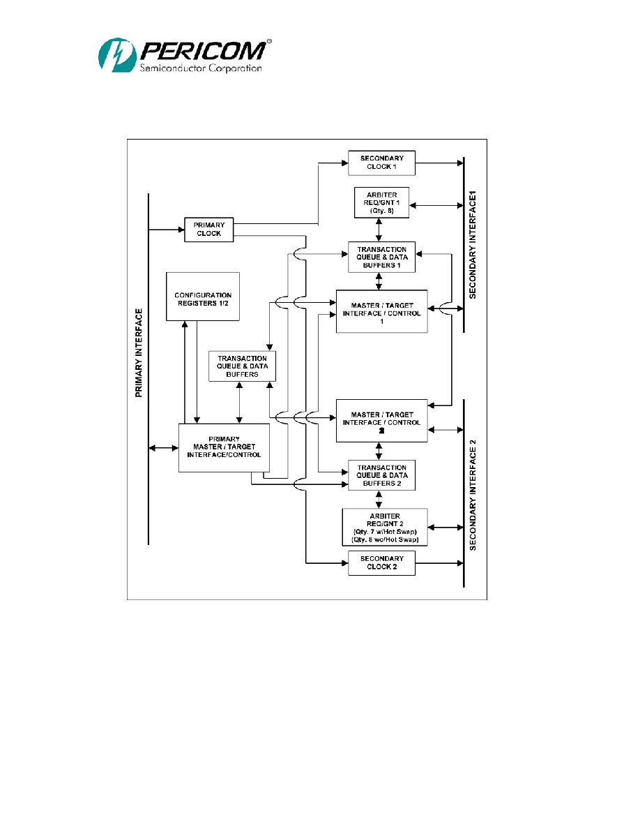
2
BLOCK DIAGRAM
PI7C7300A
3-PORT PCI-TO-PCI BRIDGE
ADVANCE INFORMATION
Page 13 OF 109
09/25/03 Revision 1.09
3
SIGNAL DEFINITIONS
3.1
SIGNAL TYPES
Signal Type
Description
PI
PCI input (3.3V, 5V tolerant)
PIU
PCI input (3.3V, 5V tolerant) with weak pull-up
PID
PCI input (3.3V, 5V tolerant) with weak pull-down
PO
PCI output (3.3V)
PB
PCI tri-state bidirectional (3.3V, 5V tolerant)
PSTS
PCI sustained tri-state bi-directional (Active LOW signal which must be driven
inactive for one cycle before being tri-stated to ensure HIGH performance on a
shared signal line)
PTS
PCI tri-state output
POD
PCI output which either drives LOW (active state) or tri-state
3.2
PRIMARY BUS INTERFACE SIGNALS
Name Pin
# Type
Description
P_AD[31:0]
Y7, W7, Y8, W8,
V8, U8, Y9, W9,
W10, V10, Y11,
V11, U11, Y12,
W12, V12, V16,
W16, Y16, W17,
Y17, U18, W18,
Y18, U19, W19,
Y19, U20, V20,
Y20, T17, R17
PB
Primary Address/Data. Multiplexed address and data
bus. Address is indicated by P_FRAME# assertion.
Write data is stable and valid when P_IRDY# is
asserted and read data is stable and valid when
P_TRDY# is asserted. Data is transferred on rising
clock edges when both P_IRDY# and P_TRDY# are
asserted. During bus idle, PI7C7300A drives P_AD to
a valid logic level when P_GNT# is asserted.
P_CBE[3:0]
V9, U12, U16,
V19
PB
Primary Command/Byte Enables. Multiplexed
command field and byte enable field. During address
phase, the initiator drives the transaction type on these
pins. The initiator then drives the byte enables during
data phases. During bus idle, PI7C7300A drives
P_CBE[3:0] to a valid logic level when P_GNT# is
asserted.
P_PAR U15
PB
Primary Parity. Parity is even across P_AD[31:0],
P_CBE[3:0], and P_PAR (i.e. an even number of 1's).
P_PAR is an input and is valid and stable one cycle
after the address phase (indicated by assertion of
P_FRAME#) for address parity. For write data phases,
P_PAR is an input and is valid one clock after
P_IRDY# is asserted. For read data phase, P_PAR is
an output and is valid one clock after P_TRDY# is
asserted. Signal P_PAR is tri-stated one cycle after the
P_AD lines are tri-stated. During bus idle, PI7C7300A
drives P_PAR to a valid logic level when P_GNT# is
asserted.
P_FRAME# W13
PSTS
Primary FRAME (Active LOW). Driven by the
initiator of a transaction to indicate the beginning and
duration of an access. The de-assertion of P_FRAME#
indicates the final data phase requested by the initiator.
Before being tri-stated, it is driven to a de-asserted
state for one cycle.

PI7C7300A
3-PORT PCI-TO-PCI BRIDGE
ADVANCE INFORMATION
Page 14 OF 109
09/25/03 Revision 1.09
Name Pin
# Type
Description
P_IRDY# V13
PSTS
Primary IRDY (Active LOW). Driven by the
initiator of a transaction to indicate its ability to
complete current data phase on the primary side. Once
asserted in a data phase, it is not de-asserted until the
end of the data phase. Before tri-stated, it is driven to a
de-asserted state for one cycle.
P_TRDY# U13
PSTS
Primary TRDY (Active LOW). Driven by the target
of a transaction to indicate its ability to complete
current data phase on the primary side. Once asserted
in a data phase, it is not de-asserted until the end of the
data phase. Before tri-stated,
it is driven to a de-asserted state for one cycle.
P_DEVSEL# Y14
PSTS
Primary Device Select (Active LOW). Asserted by
the target indicating that the device is accepting the
transaction. As a master, PI7C7300A waits for the
assertion of this signal within 5 cycles of P_FRAME#
assertion; otherwise, terminate with master abort.
Before tri-stated, it is driven to a
de-asserted state for one cycle.
P_STOP# W14
PSTS
Primary STOP (Active LOW). Asserted by the target
indicating that the target is requesting the initiator to
stop the current transaction. Before tri-stated, it is
driven to a de-asserted state for one cycle.
P_LOCK# V14
PSTS
Primary LOCK (Active LOW). Asserted by the
master for multiple transactions to complete.
P_IDSEL Y10
PI
Primary ID Select. Used as a chip select line for Type
0 configuration accesses to PI7C7300A configuration
space.
P_PERR# Y15
PSTS
Primary Parity Error (Active LOW). Asserted when
a data parity error is detected for data received on the
primary interface. Before being tri-stated, it is driven
to a de-asserted state for one cycle.
P_SERR# W15
POD
Primary System Error (Active LOW). Can be
driven LOW by any device to indicate a system error
condition. PI7C7300A drives this pin on:
!
Address parity error
!
Posted write data parity error on target bus
!
Secondary S1_SERR# or S2_SERR# asserted
!
Master abort during posted write transaction
!
Target abort during posted write transaction
!
Posted write transaction discarded
!
Delayed write request discarded
!
Delayed read request discarded
!
Delayed transaction master timeout
This signal requires an external pull-up resistor for
proper operation.
P_REQ# W6
PTS
Primary Request (Active LOW). This is asserted by
PI7C7300A to indicate that it wants to start a
transaction on the primary bus. PI7C7300A de-asserts
this pin for at least 2 PCI clock cycles before asserting
it again.
P_GNT# U7
PI
Primary Grant (Active LOW). When asserted,
PI7C7300A can access the primary bus. During idle
and P_GNT# asserted, PI7C7300A will drive P_AD,
P_CBE, and P_PAR to valid logic levels.
P_RESET# Y5
PI Primary RESET (Active LOW).
When P_RESET# is active, all PCI signals should be
asynchronously tri-stated.

PI7C7300A
3-PORT PCI-TO-PCI BRIDGE
ADVANCE INFORMATION
Page 15 OF 109
09/25/03 Revision 1.09
Name Pin
# Type
Description
P_M66EN V18
PI Primary Interface 66MHz Operation.
This input is used to specify if PI7C7300A is capable
of running at 66MHz. For 66MHz operation on the
Primary bus, this signal should be pulled "HIGH". For
33MHz operation on the Primary bus, this signal
should be pulled "LOW". In this condition,
S1_M66EN and S2_M66EN will both need to be
"LOW", forcing both secondary buses to run at 33MHz
also.
3.3
SECONDARY BUS INTERFACE SIGNALS
Name Pin
# Type
Description
S1_AD[31:0],
S2_AD[31:0]
B20, B19, C20,
C19, C18, D20,
D19, D17, E19,
E18, E17, F20,
F19, F17, G20,
G19, L20, L19,
L18, M20, M19,
M17, N20, N19,
N18, N17, P17,
R20, R19, R18,
T20, T19
J4, H1, H2, H3,
H4, G1, G3, G4,
F2, F3, F4, E1, E4,
D1, C1, B1, C5,
B5, D6, C6, B6,
A6, C7, B7, D8,
C8, D9, C9, B9,
A9, D10, C10
PB
Secondary Address/Data. Multiplexed address and
data bus. Address is indicated by S1_FRAME# or
S2_FRAME# assertion. Write data is stable and valid
when S1_IRDY# or S2_IRDY# is asserted and read
data is stable and valid when S1_IRDY# or S2_IRDY#
is asserted. Data is transferred on rising clock edges
when both S1_IRDY# or S2_IRDY# and S1_TRDY#
or S2_TRDY# are asserted. During bus idle,
PI7C7300A drives S1_AD or S2_AD to a valid logic
level when S1_GNT# or S2_GNT# is asserted
respectively.
S1_CBE[3:0],
S2_CBE[3:0]
E20, G18, K17,
P20
F1, A1, A4, A7
PB
Secondary Command/Byte Enables. Multiplexed
command field and byte enable field. During address
phase, the initiator drives the transaction type on these
pins. The initiator then drives the byte enables during
data phases. During bus idle, PI7C7300A drives
S1_CBE[3:0] or S2_CBE[3:0] to a valid logic level
when the internal grant is asserted.
S1_PAR,
S2_PAR
K18,
B4
PB
Secondary Parity. Parity is even across S1_AD[31:0],
S1_CBE[3:0], and S1_PAR or S2_AD[31:0],
S2_CBE[3:0], and S2_PAR (i.e. an even number of
1's). S1_PAR or S2_PAR is an input and is valid and
stable one cycle after the address phase (indicated by
assertion of S1_FRAME# or S2_FRAME#) for address
parity. For write data phases, S1_PAR or S2_PAR is
an input and is valid one clock after S1_IRDY#
S2_IRDY# is asserted. For read data phase, S1_PAR
or S2_PAR is an output and is valid one clock after
S1_TRDY# or S2_TRDY# is asserted. Signal S1_PAR
or S2_PAR is tri-stated one cycle after the S1_AD or
S2_AD lines are tri-stated. During bus idle,
PI7C7300A drives S1_PAR or S2_PAR to a valid logic
level when the internal grant is asserted.
S1_FRAME#,
S2_FRAME#
H20,
D2
PSTS
Secondary FRAME (Active LOW). Driven by the
initiator of a transaction to indicate the beginning and
duration of an access. The de-assertion of
S1_FRAME# or S2_FRAME# indicates the final data
phase requested by the initiator. Before being tri-
stated, it is driven to a de-asserted state for one cycle.

PI7C7300A
3-PORT PCI-TO-PCI BRIDGE
ADVANCE INFORMATION
Page 16 OF 109
09/25/03 Revision 1.09
Name Pin
# Type
Description
S1_IRDY#,
S2_IRDY#
H19,
B2
PSTS
Secondary IRDY (Active LOW). Driven by the
initiator of a transaction to indicate its ability to
complete current data phase on the secondary side.
Once asserted in a data phase, it is not de-asserted until
the end of the data phase. Before tri-stated, it is driven
to a de-asserted state for one cycle.
S1_TRDY#,
S2_TRDY#
H18,
A2
PSTS
Secondary TRDY (Active LOW). Driven by the
target of a transaction to indicate its ability to complete
current data phase on the secondary side. Once
asserted in a data phase, it is not de-asserted until the
end of the data phase. Before tri-stated, it is driven to a
de-asserted state for one cycle.
S1_DEVSEL#,
S2_DEVSEL#
J20,
D3
PSTS
Secondary Device Select (Active LOW). Asserted by
the target indicating that the device is accepting the
transaction. As a master, PI7C7300A waits for the
assertion of this signal within 5 cycles of S1_FRAME#
or S2_FRAME# assertion; otherwise, terminate with
master abort. Before tri-stated, it is driven to a de-
asserted state for one cycle.
S1_STOP#,
S2_STOP#
J19,
C3
PSTS
Secondary STOP (Active LOW). Asserted by the
target indicating that the target is requesting the
initiator to stop the current transaction. Before tri-
stated, it is driven to a de-asserted state for one cycle.
S1_LOCK#,
S2_LOCK#
J18,
B3
PSTS
Secondary LOCK (Active LOW). Asserted by the
master for multiple transactions to complete.
S1_PERR#,
S2_PERR#
J17,
D4
PSTS
Secondary Parity Error (Active LOW). Asserted
when a data parity error is detected for data received on
the secondary interface. Before being tri-stated, it is
driven to a de-asserted state for one cycle.
S1_SERR#,
S2_SERR#
K20,
C4
PI
Secondary System Error (Active LOW). Can be
driven LOW by any device to indicate a system error
condition.
S1_REQ#[7:0],
S2_REQ#[6:0]
B11, A12, D13,
C13, C15, A16,
C17, B17
R3, P2, P1, M2,
M1, K1, K3
PIU
Secondary Request (Active LOW). This is asserted
by an external device to indicate that it wants to start a
transaction on the secondary bus. The input is
externally pulled up through a resistor to VDD.
S1_GNT#[7:0]
S2_GNT#[6:0]
C11, B12, B13,
A14, D14, B16,
D16, B18
P4, R1, N4, M3,
L4, L1, K2
PO
Secondary Grant (Active LOW). PI7C7300A asserts
this pin to access the secondary bus. PI7C7300A de-
asserts this pin for at least 2 PCI clock cycles before
asserting it again. During idle and S1_GNT# or S2-
GNT# asserted, PI7C7300A will drive S1_AD,
S1_CBE, and S1_PAR or S2_AD, S2_CBE, and
S2_PAR.
S1_RESET#,
S2_RESET#
B10,
T4
PO
Secondary RESET (Active LOW). Asserted when
any of the following conditions are met:
1.
Signal P_RESET# is asserted.
2.
Secondary reset bit in bridge control register in
configuration space is set.
When asserted, all control signals are tri-stated and
zeroes are driven on S1_AD, S1_CBE, and S1_PAR or
S2_AD, S2_CBE, and S2_PAR.
S1_EN,
S2_EN
W3,
W4
PIU
Secondary Enable (Active HIGH). When S1_EN or
S2_EN is inactive, secondary bus PCI S1 or PCI S2
will be asynchronously tri-stated.
S1_M66EN,
S2_M66EN
D7,
W5
PI
Secondary Interface 66MHz Operation. This input
is used to specify if PI7C7300A is capable of running
at 66MHz on the secondary side. When HIGH, the S1
or S2 bus may run at 66MHz. When LOW, the S1 or
S2 bus may only run at 33MHz.
If P_M66EN is pulled LOW, both S1_M66EN and
S2_M66EN need to be LOW.

PI7C7300A
3-PORT PCI-TO-PCI BRIDGE
ADVANCE INFORMATION
Page 17 OF 109
09/25/03 Revision 1.09
Name Pin
# Type
Description
S_CFN# Y2
PIU
Secondary Bus Central Function Control Pin. When
tied LOW, it enables the internal arbiter. When tied
HIGH, an external arbiter must be used. S1_REQ#[0]
or S2_REQ#[0] is reconfigured to be the secondary bus
grant input, and S1_GNT#[0] or S2_GNT#[0] is
reconfigured to be the secondary bus request output.
3.4
CLOCK SIGNALS
Name Pin
# Type
Description
P_CLK V6
PI
Primary Clock Input. Provides timing for all
transactions on the primary interface.
S1_CLKOUT
[7:0]
A11, C12, A13,
B14, B15, C16,
A18, A19
PTS
Secondary Clock Output. Provides secondary 1
clocks phase synchronous with the P_CLK.
S2_CLKOUT
[7:0]
T3, T1, P3, N3,
M4, L3, L2, J1
PTS
Secondary Clock Output. Provides secondary 2
clocks phase synchronous with the P_CLK.
3.5
MISCELLANEOUS SIGNALS
Name Pin
# Type
Description
BYPASS Y4
PI
Reserved. Reserved for future use. Must be tied
HIGH.
PLL_TM Y3
PI
Reserved. Reserved for future use. Must be tied
LOW.
S_CLKIN V5
PI
Reserved. Reserved for future use. Must be tied
LOW.
SCAN_TM# V4
PI Full-Scan Test Mode Enable (Active LOW).
Connect HIGH for normal operation.
When SCAN_TM# is active, the ten scan chains will be
enabled. The scan clock is P_CLK. The scan input and
outputs are as follows:
S1_REQ[6], S1_REQ[5], S1_REQ[4], S1_REQ[3],
S1_REQ[2], S2_REQ#[6], S2_REQ#[5], S2_REQ#[4],
S2_REQ#[3], S2_REQ#[2], and S1_GNT#[6],
S1_GNT#[5], S1_GNT#[4], S1_GNT#[3],
S1_GNT#[2], S2_GNT#[6], S2_GNT#[5],
S2_GNT#[4], S2_GNT#[3], S2_GNT#[2]
SCAN_EN U5
PID
Full-Scan Enable Control. SCAN_EN should be tied
LOW in normal mode. When SCAN_EN is LOW, full-
scan is in shift operation if SCAN_TM# is active.
When SCAN_EN is HIGH, full-scan is in parallel
operation if SCAN_TM# is active.
3.6
COMPACT PCI HOT-SWAP SIGNALS
Name Pin
# Type
Description
LOO U1
PO
Hot Swap LED. The output of this pin lights a blue
LED to indicate insertion and removal ready status. If
HS_EN is LOW, pin is S2_GNT#[7].
HS_SW# T2
PI
Hot Swap Switch. When driven LOW, this signal
indicates that the board ejector handle indicates an
insertion or impending extraction of a board. If HS_EN
is LOW, pin is S2_REQ#[7].
HS_EN U6
PI
Hot Swap Enable. To enable Hot Swap Friendly
support, this signal should be pulled HIGH.

PI7C7300A
3-PORT PCI-TO-PCI BRIDGE
ADVANCE INFORMATION
Page 18 OF 109
09/25/03 Revision 1.09
Name Pin
# Type
Description
ENUM# R4
POD
Hot Swap Status Indicator. The output of ENUM#
indicates to the system that an insertion has occurred of
that an extraction is about to occur.
3.7
JTAG BOUNDARY SCAN SIGNALS
Name Pin
# Type
Description
TCK V2
PIU
Test Clock. Used to clock state information and data
into and out of the PI7C7300A during boundary scan.
TMS W1
PIU
Test Mode Select. Used to control the state of the Test
Access Port controller.
TDO V3
PTS
Test Data Output. When SCAN_EN is HIGH, it is
used (in conjunction with TCK) to shift data out of the
Test Access Port (TAP) in a serial bit stream.
TDI W2 PIU
Test Data Input. When SCAN_EN is HIGH, it is used
(in conjunction with TCK) to shift data and instructions
into the Test Access Port (TAP) in a serial bit stream.
TRST# U3
PIU
Test Reset. Active LOW signal to reset the Test
Access Port (TAP) controller into an initialized state.
3.8
POWER AND GROUND
Name Pin
# Type
Description
VDD
B8, C14, D5, D11,
D15, E2, F18, J3,
L17, N2, P19,
U10, V1, V7, V15,
W20
3.3V Digital Power
VSS
A3, A5, A8, A10,
A15, A17, A20,
C2, D12, D18, E3,
G2, G17, H17, J2,
J9, J10, J11, J12,
K4, K9, K10, K11,
K12, K19, L9,
L10, L11, L12,
M9, M10, M11,
M12, M18, N1,
P18, R2, T18, U2,
U9, U14, U17,
V17, W11, Y6,
Y13
Digital Ground
AVCC Y1
Analog 3.3V for PLL
AGND U4
Analog Ground for PLL
3.9
PI7C7300A PBGA PIN LIST
Pin #
Name
Type
Pin #
Name
Type
A1 S2_CBE[2]
PB
A2 S2_TRDY#
PSTS
A3 VSS - A4 S2_CBE[1]
PB
A5 VSS - A6 S2_AD[10]
PB
A7 S2_CBE[0]
PB
A8 VSS -
A9 S2_AD[2]
PB
A10 VSS -
A11 S1_CLKOUT[7]
PTS
A12 S1_REQ#[6]
PIU
A13 S1_CLKOUT[5]
PTS
A14 S1_GNT#[4]
PO
A15 VSS - A16 S1_REQ#[2]
PIU

PI7C7300A
3-PORT PCI-TO-PCI BRIDGE
ADVANCE INFORMATION
Page 19 OF 109
09/25/03 Revision 1.09
Pin #
Name
Type
Pin #
Name
Type
A17 VSS - A18 S1_CLKOUT[1]
PTS
A19 S1_CLKOUT[0]
PTS
A20 VSS -
B1 S2_AD[16]
PB
B2 S2_IRDY#
PSTS
B3 S2_LOCK#
PSTS
B4 S2_PAR
PB
B5 S2_AD[14]
PB
B6 S2_AD[11]
PB
B7 S2_AD[8]
PB
B8 VDD -
B9 S2_AD[3]
PB
B10 S1_RESET#
PO
B11 S1_REQ#[7]
PIU
B12 S1_GNT#[6]
PO
B13 S1_GNT#[5]
PO B14 S1_CLKOUT[4]
PTS
B15 S1_CLKOUT[3]
PTS
B16 S1_GNT#[2]
PO
B17 S1_REQ#[0]
PIU
B18 S1_GNT#[0]
PO
B19 S1_AD[30]
PB B20 S1_AD[31]
PB
C1 S2_AD[17]
PB
C2 VSS -
C3 S2_STOP#
PSTS
C4 S2_SERR#
PI
C5 S2_AD[15]
PB
C6 S2_AD[12]
PB
C7 S2_AD[9]
PB
C8 S2_AD[6]
PB
C9
S2_AD[4] PB C10
S2_AD[0] PB
C11 S1_GNT#[7]
PO C12 S1_CLKOUT[6]
PTS
C13 S1_REQ#[4]
PIU
C14 VDD PTS
C15 S1_REQ#[3]
PIU
C16 S1_CLKOUT[2]
PTS
C17 S1_REQ#[1]
PIU
C18 S1_AD[27]
PB
C19 S1_AD[28]
PB C20 S1_AD[29]
PB
D1 S2_AD[18]
PB
D2 S2_FRAME#
PSTS
D3 S2_DEVSEL#
PSTS
D4 S2_PERR#
PSTS
D5 VDD - D6 S2_AD[13]
PB
D7 S1_M66EN
PI
D8 S2_AD[7]
PB
D9
S2_AD[5] PB D10
S2_AD[1] PB
D11 VDD - D12 VSS -
D13 S1_REQ#[5]
PIU
D14 S1_GNT#[3]
PO
D15 VDD - D16 S1_GNT#[1]
PO
D17 S1_AD[24]
PB D18 VSS -
D19 S1_AD[25]
PB D20 S1_AD[26]
PB
E1 S2_AD[20]
PB
E2 VDD -
E3 VSS - E4 S2_AD[19]
PB
E17 S1_AD[21]
PB E18 S1_AD[22]
PB
E19 S1_AD[23]
PB E20 S1_CBE[3]
PB
F1 S2_CBE[3]
PB
F2 S2_AD[23]
PB
F3 S2_AD[22]
PB
F4 S2_AD[21]
PB
F17 S1_AD[18]
PB
F18 VDD -
F19 S1_AD[19]
PB
F20 S1_AD[20]
PB
G1 S2_AD[26]
PB
G2 VSS -
G3 S2_AD[25]
PB
G4 S2_AD[24]
PB
G17 VSS - G18 S1_CBE[2]
PB
G19 S1_AD[16]
PB G20 S1_AD[17]
PB
H1 S2_AD[30]
PB
H2 S2_AD[29]
PB
H3 S2_AD[28]
PB
H4 S2_AD[27]
PB
H17 VSS - H18 S1_TRDY#
PSTS
H19 S1_IRDY#
PSTS
H20 S1_FRAME#
PSTS
J1 S2_CLKOUT[0]
PTS
J2 VSS -
J3 VDD - J4 S2_AD[31]
PB
J9 VSS - J10 VSS -
J11 VSS - J12 VSS -
J17 S1_PERR#
PSTS
J18 S1_LOCK#
PSTS
J19 S1_STOP#
PSTS
J20 S1_DEVSEL#
PSTS
K1 S2_REQ#[1]
PIU
K2 S2_GNT#[0]
PO
K3 S2_REQ#[0]
PIU
K4 VSS -
K9 VSS - K10
VSS -
K11 VSS - K12 VSS -
K17 S1_CBE[1]
PB K18 S1_PAR
PB
K19 VSS - K20 S1_SERR#
PI
L1 S2_GNT#[1]
PO
L2 S2_CLKOUT[1]
PTS
L3 S2_CLKOUT[2]
PTS
L4 S2_GNT#[2]
PO
L9 VSS - L10
VSS -

PI7C7300A
3-PORT PCI-TO-PCI BRIDGE
ADVANCE INFORMATION
Page 20 OF 109
09/25/03 Revision 1.09
Pin #
Name
Type
Pin #
Name
Type
L11 VSS - L12 VSS -
L17 VDD - L18 S1_AD[13]
PB
L19 S1_AD[14]
PB L20 S1_AD[15]
PB
M1 S2_REQ#[2]
PIU
M2 S2_REQ#[3]
PIU
M3 S2_GNT#[3]
PO
M4 S2_CLKOUT[3]
PTS
M9 VSS - M10
VSS -
M11 VSS - M12 VSS -
M17 S1_AD[10]
PB M18 VSS -
M19 S1_AD[11]
PB M20 S1_AD[12]
PB
N1 VSS - N2 VDD -
N3 S2_CLKOUT[4]
PTS
N4 S2_GNT#[4]
PO
N17 S1_AD[6]
PB N18 S1_AD[7]
PB
N19 S1_AD[8]
PB N20 S1_AD[9]
PB
P1 S2_REQ#[4]
PIU
P2 S2_REQ#[5]
PIU
P3 S2_CLKOUT[5]
PTS
P4 S2_GNT#[6]
PO
P17 S1_AD[5]
PB
P18 VSS -
P19 VDD - P20 S1_CBE[0]
PB
R1 S2_GNT#[5]
PO
R2 VSS -
R3 S2_REQ#[6]
PIU
R4 ENUM#
POD
R17 P_AD[0]
PB R18 S1_AD[2]
PB
R19 S1_AD[3]
PB R20 S1_AD[4]
PB
T1 S2_CLKOUT[6]
PTS
T2 HS_SW
PI
T3 S2_CLKOUT[7]
PTS
T4 S2_RESET#
PO
T17 P_AD[1]
PB T18 VSS -
T19 S1_AD[0]
PB T20 S1_AD[1]
PB
U1 LOO PO
U2 VSS -
U3 TRST#
PIU
U4 AGND
-
U5 SCAN_EN
PID
U6 HS_EN
PI
U7 P_GNT#
PI
U8 P_AD[26]
PB
U9 VSS - U10 VDD -
U11 P_AD[19]
PB U12 P_CBE[2]
PB
U13 P_TRDY#
PB U14 VSS -
U15 P_PAR PB U16 P_CBE[1]
PB
U17 VSS - U18 P_AD[10]
PB
U19 P_AD[7]
PB U20 P_AD[4]
PB
V1 VDD - V2 TCK PIU
V3 TDO PTS
V4 SCAN_TM#
PI
V5 S_CLKIN
PI
V6 P_CLK
PI
V7 VDD - V8 P_AD[27]
PB
V9
P_CBE[3] PB V10
P_AD[22] PB
V11 P_AD[20]
PB V12 P_AD[16]
PB
V13 P_IRDY#
PB V14 P_LOCK#
PSTS
V15 VDD - V16 P_AD[15]
PB
V17 VSS - V18 P_M66EN#
PI
V19 P_CBE[0]
PB V20 P_AD[3]
PB
W1 TMS PIU
W2 TDI PIU
W3 S1_EN PIU
W4 S2_EN PIU
W5 S2_M66EN
PI W6 P_REQ#
PTS
W7 P_AD[30]
PB
W8 P_AD[28]
PB
W9
P_AD[24] PB W10
P_AD[23] PB
W11 VSS - W12 P_AD[17]
PB
W13 P_FRAME#
PB W14 P_STOP#
PSTS
W15 P_SERR#
POD
W16 P_AD[14]
PB
W17 P_AD[12]
PB W18 P_AD[9]
PB
W19 P_AD[6]
PB W20 VDD -
Y1 AVCC
- Y2 S_CFN#
PIU
Y3 PLL_TM
PI
Y4 BYPASS
-
Y5 P_RESET#
PI
Y6 VSS -
Y7 P_AD[31]
PB
Y8 P_AD[29]
PB
Y9 P_AD[25]
PB
Y10 P_IDSEL
PI
Y11 P_AD[21]
PB Y12 P_AD[18]
PB
Y13 VSS - Y14 P_DEVSEL#
PSTS
Y15 P_PERR#
PSTS
Y16 P_AD[13]
PB

PI7C7300A
3-PORT PCI-TO-PCI BRIDGE
ADVANCE INFORMATION
Page 21 OF 109
09/25/03 Revision 1.09
Pin #
Name
Type
Pin #
Name
Type
Y17 P_AD[11]
PB Y18 P_AD[8]
PB
Y19 P_AD[5]
PB Y20 P_AD[2]
PB
4
PCI BUS OPERATION
This Chapter offers information about PCI transactions, transaction forwarding across
PI7C7300A, and transaction termination. The PI7C7300A has three 128-byte buffers for
buffering of upstream and downstream transactions. These hold addresses, data,
commands, and byte enables and are used for both read and write transactions.
4.1
TYPES OF TRANSACTIONS
This section provides a summary of PCI transactions performed by PI7C7300A.
Table 4-1 lists the command code and name of each PCI transaction. The Master and
Target columns indicate support for each transaction when PI7C7300A initiates
transactions as a master, on the primary (P) and secondary (S1, S2) buses, and when
PI7C7300A responds to transactions as a target, on the primary (P) and secondary (S1,
S2) buses.
Table 4-1 PCI TRANSACTIONS
Types of Transactions
Initiates as Master
Responds as Target
Primary
Secondary
Primary
Secondary
0000 Interrupt
Acknowledge
N
N
N
N
0001 Special
Cycle
Y
Y
N
N
0010 I/O
Read
Y
Y
Y
Y
0011 I/O
Write
Y
Y
Y
Y
0100 Reserved
N
N
N
N
0101 Reserved
N
N
N
N
0110 Memory
Read
Y
Y
Y
Y
0111 Memory
Write
Y
Y
Y
Y
1000 Reserved
N
N
N
N
1001 Reserved
N
N
N
N
1010 Configuration
Read
N
Y
Y
N
1011
Configuration Write
Y (Type 1 only)
Y
Y
Y (Type 1 only)
1100
Memory Read Multiple
Y
Y
Y
Y
1101
Dual Address Cycle
Y
Y
Y
Y
1110
Memory Read Line
Y
Y
Y
Y
1111
Memory Write and Invalidate
Y
Y
Y
Y
As indicated in Table 4-1, the following PCI commands are not supported by
PI7C7300A:
!
PI7C7300A never initiates a PCI transaction with a reserved command code and, as
a target, PI7C7300A ignores reserved command codes.
!
PI7C7300A does not generate interrupt acknowledge transactions. PI7C7300A
ignores interrupt acknowledge transactions as a target.
!
PI7C7300A does not respond to special cycle transactions. PI7C7300A cannot
guarantee delivery of a special cycle transaction to downstream buses because of the

PI7C7300A
3-PORT PCI-TO-PCI BRIDGE
ADVANCE INFORMATION
Page 22 OF 109
09/25/03 Revision 1.09
broadcast nature of the special cycle command and the inability to control the
transaction as a target. To generate special cycle transactions on other PCI buses,
either upstream or downstream, Type 1 configuration write must be used.
!
PI7C7300A neither generates Type 0 configuration transactions on the primary PCI
bus nor responds to Type 0 configuration transactions on the secondary PCI buses.
4.2
SINGLE ADDRESS PHASE
A 32-bit address uses a single address phase. This address is driven on P_AD[31:0], and
the bus command is driven on P_CBE[3:0]. PI7C7300A supports the linear increment
address mode only, which is indicated when the lowest two address bits are equal to zero.
If either of the lowest two address bits is nonzero, PI7C7300A automatically disconnects
the transaction after the first data transfer.
4.3
DUAL ADDRESS PHASE
A 64-bit address uses two address phases. The first address phase is denoted by
the asserting edge of FRAME#. The second address phase always follows on the
next clock cycle.
For a 32-bit interface, the first address phase contains dual address command code on the
C/BE#[3:0] lines, and the low 32 address bits on the AD[31:0] lines. The second address
phase consists of the specific memory transaction command code on the C/BE#[3:0]
lines, and the high 32 address bits on the AD[31:0] lines. In this way, 64-bit addressing
can be supported on 32-bit PCI buses.
The PCI-to-PCI Bridge Architecture Specification supports the use of dual address
transactions in the prefetchable memory range only. See Section 5.3.2 for a discussion of
prefetchable address space. The PI7C7300A supports dual address transactions in both
the upstream and the downstream direction. The PI7C7300A supports a programmable
64-bit address range in prefetchable memory for downstream forwarding of dual address
transactions. Dual address transactions falling outside the prefetchable address range are
forwarded upstream, but not downstream. Prefetching and posting are performed in a
manner consistent with
the guidelines given in this specification for each type of memory transaction in
prefetchable memory space.
4.4
DEVICE SELECT (DEVSEL#) GENERATION
PI7C7300A always performs positive address decoding (medium decode) when
accepting transactions on either the primary or secondary buses. PI7C7300A never does
subtractive decode.
4.5
DATA PHASE
The address phase of a PCI transaction is followed by one or more data phases.
A data phase is completed when IRDY# and either TRDY# or STOP# are asserted.
PI7C7300A
3-PORT PCI-TO-PCI BRIDGE
ADVANCE INFORMATION
Page 23 OF 109
09/25/03 Revision 1.09
A transfer of data occurs only when both IRDY# and TRDY# are asserted during the
same PCI clock cycle. The last data phase of a transaction is indicated when FRAME# is
de-asserted and both TRDY# and IRDY# are asserted, or when IRDY# and STOP# are
asserted. See Section 4.9 for further discussion of transaction termination.
Depending on the command type, PI7C7300A can support multiple data phase
PCI transactions. For detailed descriptions of how PI7C7300A imposes disconnect
boundaries, see Section 4.6.4 for write address boundaries and Section 4.7.3 read address
boundaries.
4.6
WRITE TRANSACTIONS
Write transactions are treated as either posted write or delayed write transactions.
Table 4-2 shows the method of forwarding used for each type of write operation.
Table 4-2 WRITE TRANSACTION FORWARDING
Type of Transaction
Type of Forwarding
Memory Write
Posted (except VGA memory)
Memory Write and Invalidate
Posted
Memory Write to VGA memory
Delayed
I/O Write
Delayed
Type 1 Configuration Write
Delayed
4.6.1
MEMORY WRITE TRANSACTIONS
Posted write forwarding is used for "Memory Write" and "Memory Write and
Invalidate" transactions.
When PI7C7300A determines that a memory write transaction is to be forwarded across
the bridge, PI7C7300A asserts DEVSEL# with medium timing and TRDY# in the next
cycle, provided that enough buffer space is available in the posted memory write queue
for the address and at least one DWORD of data. Under this condition, PI7C7300A
accepts write data without obtaining access to the target bus. The PI7C7300A can accept
one DWORD of write data every PCI clock cycle. That is, no target wait state is inserted.
The write data is stored in an internal posted write buffers and is subsequently delivered
to the target. The PI7C7300A continues to accept write data until one of the following
events occurs:
!
The initiator terminates the transaction by de-asserting FRAME# and IRDY#.
!
An internal write address boundary is reached, such as a cache line boundary or an
aligned 4KB boundary, depending on the transaction type.
!
The posted write data buffer fills up.
When one of the last two events occurs, the PI7C7300A returns a target disconnect to the
requesting initiator on this data phase to terminate the transaction.
Once the posted write data moves to the head of the posted data queue, PI7C7300A
asserts its request on the target bus. This can occur while PI7C7300A is still receiving
data on the initiator bus. When the grant for the target bus is received and the target bus
is detected in the idle condition, PI7C7300A asserts FRAME# and drives the stored write

PI7C7300A
3-PORT PCI-TO-PCI BRIDGE
ADVANCE INFORMATION
Page 24 OF 109
09/25/03 Revision 1.09
address out on the target bus. On the following cycle, PI7C7300A drives the first
DWORD of write data and continues to transfer write data until all write data
corresponding to that transaction is delivered, or until a target termination is received. As
long as write data exists in the queue, PI7C7300A can drive one DWORD of write data
each PCI clock cycle; that is, no master wait states are inserted. If write data is flowing
through PI7C7300A and the initiator stalls, PI7C7300A will signal the last data phase for
the current transaction at the target bus if the queue empties. PI7C7300A will restart the
follow-on transactions if the queue has new data.
PI7C7300A ends the transaction on the target bus when one of the following conditions
is met:
!
All posted write data has been delivered to the target.
!
The target returns a target disconnect or target retry (PI7C7300A starts another
transaction to deliver the rest of the write data).
!
The target returns a target abort (PI7C7300A discards remaining write data).
!
The master latency timer expires, and PI7C7300A no longer has the target bus grant
(PI7C7300A starts another transaction to deliver remaining write data).
Section 4.9.3.2 provides detailed information about how PI7C7300A responds to target
termination during posted write transactions.
4.6.2
MEMORY WRITE AND INVALIDATE TRANSACTIONS
Posted write forwarding is used for Memory Write and Invalidate transactions.
The PI7C7300A disconnects Memory Write and Invalidate commands at aligned cache
line boundaries. The cache line size value in the cache line size register gives the number
of DWORD in a cache line.
If the value in the cache line size register does meet the memory write and invalidate
conditions, the PI7C7300A returns a target disconnect to the initiator either on a cache
line boundary or when the posted write buffer fills.
When the Memory Write and Invalidate transaction is disconnected before a cache line
boundary is reached, typically because the posted write buffer fills, the trans-action is
converted to Memory Write transaction.
4.6.3
DELAYED WRITE TRANSACTIONS
Delayed write forwarding is used for I/O write transactions and Type 1 configuration
write transactions.
A delayed write transaction guarantees that the actual target response is returned back to
the initiator without holding the initiating bus in wait states. A delayed write transaction
is limited to a single DWORD data transfer.

PI7C7300A
3-PORT PCI-TO-PCI BRIDGE
ADVANCE INFORMATION
Page 25 OF 109
09/25/03 Revision 1.09
When a write transaction is first detected on the initiator bus, and PI7C7300A forwards it
as a delayed transaction, PI7C7300A claims the access by asserting DEVSEL# and
returns a target retry to the initiator. During the address phase, PI7C7300A samples the
bus command, address, and address parity one cycle later. After IRDY# is asserted,
PI7C7300A also samples the first data DWORD, byte enable bits, and data parity. This
information is placed into the delayed transaction queue. The transaction is queued only
if no other existing delayed transactions have the same address and command, and if the
delayed transaction queue is not full. When the delayed write transaction moves to the
head of the delayed transaction queue and all ordering constraints with posted data are
satisfied. The PI7C7300A initiates the transaction on the target bus. PI7C7300A
transfers the write data to the target. If PI7C7300A receives a target retry
in response to the write transaction on the target bus, it continues to repeat the write
transaction until the data transfer is completed, or until an error condition is encountered.
If PI7C7300A is unable to deliver write data after 2
24
(default) or 2
32
(maximum)
attempts, PI7C7300A will report a system error. PI7C7300A also asserts P_SERR# if the
primary SERR# enable bit is set in the command register. See Section 7.4 for information
on the assertion of P_SERR#. When the initiator repeats the same write transaction (same
command, address, byte enable bits, and data), and the completed delayed transaction is
at the head of the queue, the PI7C7300A claims the access by asserting DEVSEL# and
returns TRDY# to the initiator, to indicate that the write data
was transferred. If the initiator requests multiple DWORD, PI7C7300A also asserts
STOP# in conjunction with TRDY# to signal a target disconnect. Note that only those
bytes of write data with valid byte enable bits are compared. If any of the byte enable bits
are turned off (driven HIGH), the corresponding byte of write data is not compared.
If the initiator repeats the write transaction before the data has been transferred to the
target, PI7C7300A returns a target retry to the initiator. PI7C7300A continues to return a
target retry to the initiator until write data is delivered to the target, or until an error
condition is encountered. When the write transaction is repeated, PI7C7300A does not
make a new entry into the delayed transaction queue. Section 4.9.3.1 provides detailed
information about how PI7C7300A responds to target termination during delayed write
transactions.
PI7C7300A implements a discard timer that starts counting when the delayed write
completion is at the head of the delayed transaction completion queue. The initial value
of this timer can be set to the retry counter register offset 78h.
If the initiator does not repeat the delayed write transaction before the discard timer
expires, PI7C7300A discards the delayed write completion from the delayed transaction
completion queue. PI7C7300A also conditionally asserts P_SERR# (see Section 7.4).
4.6.4
WRITE TRANSACTION ADDRESS BOUNDARIES
PI7C7300A imposes internal address boundaries when accepting write data. The aligned
address boundaries are used to prevent PI7C7300A from continuing a transaction over a
device address boundary and to provide an upper limit on maximum latency. PI7C7300A
returns a target disconnect to the initiator when it reaches the aligned address boundaries
under conditions shown in Table 43.

PI7C7300A
3-PORT PCI-TO-PCI BRIDGE
ADVANCE INFORMATION
Page 26 OF 109
09/25/03 Revision 1.09
Table 4-3 WRITE TRANSACTION DISCONNECT ADDRESS BOUNDARIES
Type of Transaction
Condition
Aligned Address Boundary
Delayed Write
All
Disconnects after one data transfer
Posted Memory Write
Memory write disconnect control
bit = 0
(1)
4KB aligned address boundary
Posted Memory Write
Memory write disconnect control
bit = 1
(1)
Disconnects at cache line boundary
Posted Memory Write and
Invalidate
Cache line size
1, 2, 4, 8, 16
4KB aligned address boundary
Posted Memory Write and
Invalidate
Cache line size = 1, 2, 4, 8, 16
Cache line boundary if posted memory
write data FIFO does not have enough
space for the cache line
Note 1. Memory write disconnect control bit is bit 1 of the chip control register at offset 40h in the
configuration space.
4.6.5
BUFFERING MULTIPLE WRITE TRANSACTIONS
PI7C7300A continues to accept posted memory write transactions as long as space for at
least one DWORD of data in the posted write data buffer remains. If the posted write
data buffer fills before the initiator terminates the write transaction, PI7C7300A returns a
target disconnect to the initiator.
Delayed write transactions are posted as long as at least one open entry in the delayed
transaction queue exists. Therefore, several posted and delayed write transactions can
exist in data buffers at the same time. See Chapter 6 for information about how multiple
posted and delayed write transactions are ordered.
4.6.6
FAST BACK-TO-BACK WRITE TRANSACTIONS
PI7C7300A can recognize and post fast back-to-back write transactions. When
PI7C7300A cannot accept the second transaction because of buffer space limitations, it
returns a target retry to the initiator. The fast back-to-back enable bit must be set in the
command register for upstream write transactions, and in the bridge control register for
downstream write transactions.
4.7
READ TRANSACTIONS
Delayed read forwarding is used for all read transactions crossing PI7C7300A. Delayed
read transactions are treated as either prefetchable or non-prefetchable. Table 4-4 shows
the read behavior, prefetchable or non-prefetchable, for each type of read operation.
4.7.1
PREFETCHABLE READ TRANSACTIONS
A prefetchable read transaction is a read transaction where PI7C7300A performs
speculative DWORD reads, transferring data from the target before it is requested from
the initiator. This behavior allows a prefetchable read transaction to consist of multiple
data transfers. However, byte enable bits cannot be forwarded for all data phases as is
done for the single data phase of the non-prefetchable read transaction. For prefetchable
read transactions, PI7C7300A forces all byte enable bits to be turned on for all data
phases.

PI7C7300A
3-PORT PCI-TO-PCI BRIDGE
ADVANCE INFORMATION
Page 27 OF 109
09/25/03 Revision 1.09
Prefetchable behavior is used for memory read line and memory read multiple
transactions, as well as for memory read transactions that fall into prefetchable memory
space. The amount of data that is pre-fetched depends on the type of transaction. The
amount of pre-fetching may also be affected by the amount of free buffer space available
in PI7C7300A, and by any read address boundaries encountered.
Pre-fetching should not be used for those read transactions that have side effects in the
target device, that is, control and status registers, FIFOs, and so on. The target device's
base address register or registers indicate if a memory address region is prefetchable.
4.7.2
NON-PREFETCHABLE READ TRANSACTIONS
A non-prefetchable read transaction is a read transaction where PI7C7300A requests one
and only one DWORD from the target and disconnects the initiator after delivery of the
first DWORD of read data. Unlike prefetchable read transactions, PI7C7300A forwards
the read byte enable information for the data phase.
Non-prefetchable behavior is used for I/O and configuration read transactions, as well as
for memory read transactions that fall into non-prefetchable memory space.
If extra read transactions could have side effects, for example, when accessing a FIFO,
use non-prefetchable read transactions to those locations. Accordingly, if it is important
to retain the value of the byte enable bits during the data phase, use non-prefetchable
read transactions. If these locations are mapped in memory space, use the memory read
command and map the target into non-prefetchable (memory-mapped I/O) memory space
to use non-prefetching behavior.
4.7.3
READ PREFETCH ADDRESS BOUNDARIES
PI7C7300A imposes internal read address boundaries on read pre-fetched data. When a
read transaction reaches one of these aligned address boundaries, the PI7C7300A stops
pre-fetched data, unless the target signals a target disconnect before the read pre-fetched
boundary is reached. When PI7C7300A finishes transferring this read data to the
initiator, it returns a target disconnect with the last data transfer, unless the initiator
completes the transaction before all pre-fetched read data is delivered. Any leftover pre-
fetched data is discarded.
Prefetchable read transactions in flow-through mode pre-fetch to the nearest aligned 4KB
address boundary, or until the initiator de-asserts FRAME#. Section 4.7.6 describes flow-
through mode during read operations.
Table 4-5 shows the read pre-fetch address boundaries for read transactions during non-
flow-through mode.
Table 4-4 READ PREFETCH ADDRESS BOUNDARIES
Type of Transaction
Address Space
Cache Line Size
(CLS)
Prefetch Aligned Address
Boundary
Configuration Read
-
*
One DWORD (no prefetch)
I/O Read
-
*
One DWORD (no prefetch)
Memory Read
Non-Prefetchable
*
One DWORD (no prefetch)
PI7C7300A
3-PORT PCI-TO-PCI BRIDGE
ADVANCE INFORMATION
Page 28 OF 109
09/25/03 Revision 1.09
Memory Read
Prefetchable
CLS = 0 or 16
16-DWORD aligned address
boundary
Memory Read
Prefetchable
CLS = 1, 2, 4, 8, 16
Cache line address boundary
Memory Read Line
-
CLS = 0 or 16
16-DWORD aligned address
boundary
Memory Read Line
-
CLS = 1, 2, 4, 8, 16
Cache line boundary
Memory Read Multiple
-
CLS = 0 or 16
32-DWORD aligned address
boundary
Memory Read Multiple
-
CLS = 1, 2, 4, 8, 16
2X of cache line boundary
- does not matter if it is prefetchable or non-prefetchable
* don't care
Table 4-5 READ TRANSACTION PREFETCHING
Type of Transaction
Read Behavior
I/O Read
Prefetching never allowed
Configuration Read
Prefetching never allowed
Downstream: Prefetching used if address is prefetchable space
Memory Read
Upstream: Prefetching used or programmable
Memory Read Line
Prefetching always used
Memory Read Multiple
Prefetching always used
See Section 5.3 for detailed information about prefetchable and non-prefetchable address spaces.
4.7.4
DELAYED READ REQUESTS
PI7C7300A treats all read transactions as delayed read transactions, which means that the
read request from the initiator is posted into a delayed transaction queue. Read data from
the target is placed in the read data queue directed toward the initiator bus interface and
is transferred to the initiator when the initiator repeats the read transaction.
When PI7C7300A accepts a delayed read request, it first samples the read address, read
bus command, and address parity. When IRDY# is asserted, PI7C7300A then samples
the byte enable bits for the first data phase. This information is entered into the delayed
transaction queue. PI7C7300A terminates the transaction by signaling a target retry to the
initiator. Upon reception of the target retry, the initiator is required to continue to repeat
the same read transaction until at least one data transfer is completed, or until a target
response (target abort or master abort) other than a target retry is received.
4.7.5
DELAYED READ COMPLETION WITH TARGET
When delayed read request reaches the head of the delayed transaction queue,
PI7C7300A arbitrates for the target bus and initiates the read transaction only if all
previously queued posted write transactions have been delivered. PI7C7300A uses the
exact read address and read command captured from the initiator during the initial
delayed read request to initiate the read transaction. If the read transaction is a non-
prefetchable read, PI7C7300A drives the captured byte enable bits during the next cycle.
If the transaction is a prefetchable read transaction, it drives all byte enable bits to zero
for all data phases. If PI7C7300A receives a target retry in response to the read
transaction on the target bus, it continues to repeat the read transaction until at least one
data transfer is completed, or until an error condition is encountered. If the transaction is
terminated via normal master termination or target disconnect after at least one data
transfer has been completed, PI7C7300A does not initiate any further attempts to read
more data.

PI7C7300A
3-PORT PCI-TO-PCI BRIDGE
ADVANCE INFORMATION
Page 29 OF 109
09/25/03 Revision 1.09
If PI7C7300A is unable to obtain read data from the target after 2
24
(default) or 2
32
(maximum) attempts, PI7C7300A will report a system error. The number of attempts is
programmable. PI7C7300A also asserts P_SERR# if the primary SERR# enable bit is set
in the command register. See Section 7.4 for information on the assertion of P_SERR#.
Once PI7C7300A receives DEVSEL# and TRDY# from the target, it transfers the data
read to the opposite direction read data queue, pointing toward the opposite inter-face,
before terminating the transaction. For example, read data in response to a downstream
read transaction initiated on the primary bus is placed in the upstream read data queue.
The PI7C7300A can accept one DWORD of read data each PCI clock cycle; that is, no
master wait states are inserted. The number of DWORD transferred during a delayed
read transaction depends on the conditions given in Table 4-5 (assuming no disconnect is
received from the target).
4.7.6
DELAYED READ COMPLETION ON INITIATOR BUS
When the transaction has been completed on the target bus, and the delayed read data is
at the head of the read data queue, and all ordering constraints with posted write
transactions have been satisfied, the PI7C7300A transfers the data to the initiator when
the initiator repeats the transaction. For memory read transactions, PI7C7300A aliases
the memory read, memory read line, and memory read multiple bus commands when
matching the bus command of the transaction to the bus command in the delayed
transaction queue. PI7C7300A returns a target disconnect along with the transfer of the
last DWORD of read data to the initiator. If PI7C7300A initiator terminates the
transaction before all read data has been transferred, the remaining read data left in data
buffers is discarded.
When the master repeats the transaction and starts transferring prefetchable read data
from data buffers while the read transaction on the target bus is still in progress and
before a read boundary is reached on the target bus, the read transaction starts operating
in flow-through mode. Because data is flowing through the data buffers from the target to
the initiator, long read bursts can then be sustained. In this case, the read transaction is
allowed to continue until the initiator terminates the trans-action, or until an aligned 4KB
address boundary is reached, or until the buffer fills, whichever comes first. When the
buffer empties, PI7C7300A reflects the stalled condition to the initiator by disconnecting
the initiator with data. The initiator may retry the transaction later if data are needed. If
the initiator does not need any more data, the initiator will not continue the disconnected
transaction. In this case, PI7C7300A will start the master timeout timer. The remaining
read data will be discarded after the master timeout timer expires. To provide better
latency, if there are any other pending data for other transactions in the RDB (Read Data
Buffer), the remaining read data will be discarded even though the master timeout timer
has not expired.
PI7C7300A implements a master timeout timer that starts counting when the delayed
read completion is at the head of the delayed transaction queue, and the read data is at the
head of the read data queue. The initial value of this timer is program-mable through
configuration register. If the initiator does not repeat the read transaction and before the
master timeout timer expires (2
15
default), PI7C7300A discards the read transaction and
read data from its queues. PI7C7300A also conditionally asserts P_SERR# (see Section
7.4).

PI7C7300A
3-PORT PCI-TO-PCI BRIDGE
ADVANCE INFORMATION
Page 30 OF 109
09/25/03 Revision 1.09
PI7C7300A has the capability to post multiple delayed read requests, up to a maximum
of four in each direction. If an initiator starts a read transaction that matches the address
and read command of a read transaction that is already queued, the current read
command is not posted as it is already contained in the delayed transaction queue.
See Section 6 for a discussion of how delayed read transactions are ordered when
crossing PI7C7300A.
4.7.7
FAST BACK-TO-BACK READ TRANSACTION
PI7C7300A can recognize fast back-to-back read transactions.
4.8
CONFIGURATION TRANSACTIONS
Configuration transactions are used to initialize a PCI system. Every PCI device
has a configuration space that is accessed by configuration commands. All registers are
accessible in configuration space only.
In addition to accepting configuration transactions for initialization of its own
configuration space, the PI7C7300A also forwards configuration transactions for device
initialization in hierarchical PCI systems, as well as for special cycle generation.
To support hierarchical PCI bus systems, two types of configuration transactions are
specified: Type 0 and Type 1.
Type 0 configuration transactions are issued when the intended target resides on the same
PCI bus as the initiator. A Type 0 configuration transaction is identified by the
configuration command and the lowest two bits of the address set to 00b.
Type 1 configuration transactions are issued when the intended target resides on another
PCI bus, or when a special cycle is to be generated on another PCI bus. A Type 1
configuration command is identified by the configuration command and the lowest two
address bits set to 01b.
The register number is found in both Type 0 and Type 1 formats and gives the DWORD
address of the configuration register to be accessed. The function number is also included
in both Type 0 and Type 1 formats and indicates which function of a multifunction
device is to be accessed. For single-function devices, this value is not decoded. The
addresses of Type 1 configuration transaction include a 5-bit field designating the device
number that identifies the device on the target PCI bus that is to be accessed. In addition,
the bus number in Type 1 transactions specifies the PCI bus to which the transaction is
targeted.
4.8.1
TYPE 0 ACCESS TO PI7C7300A
The configuration space is accessed by a Type 0 configuration transaction on the primary
interface. The configuration space cannot be accessed from the secondary bus. The
PI7C7300A responds to a Type 0 configuration transaction by asserting P_DEVSEL#
when the following conditions are met during the address phase:

PI7C7300A
3-PORT PCI-TO-PCI BRIDGE
ADVANCE INFORMATION
Page 31 OF 109
09/25/03 Revision 1.09
!
The bus command is a configuration read or configuration write transaction.
!
Lowest two address bits P_AD[1:0] must be 00b.
!
Signal P_IDSEL must be asserted.
Function code is either 0 for configuration space of S1, or 1 for configuration space of S2
as PI7C7300A is a multi-function device.
PI7C7300A limits all configuration access to a single DWORD data transfer and returns
target-disconnect with the first data transfer if additional data phases are requested.
Because read transactions to configuration space do not have side effects, all bytes in the
requested DWORD are returned, regardless of the value of the byte enable bits.
Type 0 configuration write and read transactions do not use data buffers; that is, these
transactions are completed immediately, regardless of the state of the data buffers. The
PI7C7300A ignores all Type 0 transactions initiated on the secondary interface.
4.8.2
TYPE 1 TO TYPE 0 CONVERSION
Type 1 configuration transactions are used specifically for device configuration in a
hierarchical PCI bus system. A PCI-to-PCI bridge is the only type of device that should
respond to a Type 1 configuration command. Type 1 configuration commands are used
when the configuration access is intended for a PCI device that resides on a PCI bus
other than the one where the Type 1 transaction is generated.
PI7C7300A performs a Type 1 to Type 0 translation when the Type 1 transaction is
generated on the primary bus and is intended for a device attached directly to the
secondary bus. PI7C7300A must convert the configuration command to a Type 0 format
so that the secondary bus device can respond to it. Type 1 to Type 0 translations are
performed only in the downstream direction; that is, PI7C7300A generates a Type 0
transaction only on the secondary bus, and never on the primary bus.
PI7C7300A responds to a Type 1 configuration transaction and translates it into a Type 0
transaction on the secondary bus when the following conditions are met during the
address phase:
!
The lowest two address bits on P_AD[1:0] are 01b.
!
The bus number in address field P_AD[23:16] is equal to the value in the secondary
bus number register in configuration space.
!
The bus command on P_CBE[3:0] is a configuration read or configuration write
transaction.
When PI7C7300A translates the Type 1 transaction to a Type 0 transaction on the
secondary interface, it performs the following translations to the address:
!
Sets the lowest two address bits on S1_AD[1:0] or S2_AD[1:0] to 00b.

PI7C7300A
3-PORT PCI-TO-PCI BRIDGE
ADVANCE INFORMATION
Page 32 OF 109
09/25/03 Revision 1.09
!
Decodes the device number and drives the bit pattern specified in Table 4-6 on
S1_AD[31:16] or S2_AD[31:16] for the purpose of asserting the device's IDSEL
signal.
!
Sets S1_AD[15:11] or S2_AD[15:11] to 0.
!
Leaves unchanged the function number and register number fields.
PI7C7300A asserts a unique address line based on the device number. These address
lines may be used as secondary bus IDSEL signals. The mapping of the address lines
depends on the device number in the Type 1 address bits P_AD[15:11]. Table 4-6
presents the mapping that PI7C7300A uses.
Table 4-6 DEVICE NUMBER TO IDSEL S1_AD OR S2_AD PIN MAPPING
Device
Number
P_AD[15:11]
Secondary IDSEL S1_AD[31:16] or
S2_AD[31:16]
S1_AD or
S2_AD
0h
00000
0000 0000 0000 0001
16
1h
00001
0000 0000 0000 0010
17
2h
00010
0000 0000 0000 0100
18
3h
00011
0000 0000 0000 1000
19
4h
00100
0000 0000 0001 0000
20
5h
00101
0000 0000 0010 0000
21
6h
00110
0000 0000 0100 0000
22
7h
00111
0000 0000 1000 0000
23
8h
01000
0000 0001 0000 0000
24
9h
01001
0000 0010 0000 0000
25
Ah
01010
0000 0100 0000 0000
26
Bh
01011
0000 1000 0000 0000
27
Ch
01100
0001 0000 0000 0000
28
Dh
01101
0010 0000 0000 0000
29
Eh
01110
0100 0000 0000 0000
30
Fh
01111
1000 0000 0000 0000
31
10h 1Eh
10000 11110
0000 0000 0000 0000
-
1Fh
11111
Generate special cycle (P_AD[7:2] = 00h)
0000 0000 0000 0000 (P_AD[7:2] = 00h)
-
PI7C7300A can assert up to 16 unique address lines to be used as IDSEL signals for up
to 16 devices on the secondary bus, for device numbers ranging from 0 through 15.
Because of electrical loading constraints of the PCI bus, more than 16 IDSEL signals
should not be necessary. However, if device numbers greater than 15 are desired, some
external method of generating IDSEL lines must be used, and no upper address bits are
then asserted. The configuration transaction is still translated and passed from the
primary bus to the secondary bus. If no IDSEL pin is asserted to a secondary device, the
transaction ends in a master abort.
PI7C7300A forwards Type 1 to Type 0 configuration read or write transactions as
delayed transactions. Type 1 to Type 0 configuration read or write transactions are
limited to a single 32-bit data transfer.
4.8.3
TYPE 1 TO TYPE 1 FORWARDING
Type 1 to Type 1 transaction forwarding provides a hierarchical configuration
mechanism when two or more levels of PCI-to-PCI bridges are used.

PI7C7300A
3-PORT PCI-TO-PCI BRIDGE
ADVANCE INFORMATION
Page 33 OF 109
09/25/03 Revision 1.09
When PI7C7300A detects a Type 1 configuration transaction intended for a PCI bus
downstream from the secondary bus, PI7C7300A forwards the transaction unchanged to
the secondary bus. Ultimately, this transaction is translated to a Type 0 configuration
command or to a special cycle transaction by a downstream PCI-to-PCI bridge.
Downstream Type 1 to Type 1 forwarding occurs when the following conditions are met
during the address phase:
!
The lowest two address bits are equal to 01b.
!
The bus number falls in the range defined by the lower limit (exclusive) in the
secondary bus number register and the upper limit (inclusive) in the subordinate bus
number register.
!
The bus command is a configuration read or write transaction.
PI7C7300A also supports Type 1 to Type 1 forwarding of configuration write
transactions upstream to support upstream special cycle generation. A Type 1
configuration command is forwarded upstream when the following conditions are met:
!
The lowest two address bits are equal to 01b.
!
The bus number falls outside the range defined by the lower limit (inclusive)
in the secondary bus number register and the upper limit (inclusive) in the
subordinate bus number register.
!
The device number in address bits AD[15:11] is equal to 11111b.
!
The function number in address bits AD[10:8] is equal to 111b.
!
The bus command is a configuration write transaction.
The PI7C7300A forwards Type 1 to Type 1 configuration write transactions as delayed
transactions. Type 1 to Type 1 configuration write transactions are limited to a single
data transfer.
4.8.4
SPECIAL CYCLES
The Type 1 configuration mechanism is used to generate special cycle transactions in
hierarchical PCI systems. Special cycle transactions are ignored by acting as a target and
are not forwarded across the bridge. Special cycle transactions can be generated from
Type 1 configuration write transactions in either the upstream or the down-stream
direction.
PI7C7300A initiates a special cycle on the target bus when a Type 1 configuration write
transaction is being detected on the initiating bus and the following conditions are met
during the address phase:
!
The lowest two address bits on AD[1:0] are equal to 01b.
!
The device number in address bits AD[15:11] is equal to 11111b.
!
The function number in address bits AD[10:8] is equal to 111b.

PI7C7300A
3-PORT PCI-TO-PCI BRIDGE
ADVANCE INFORMATION
Page 34 OF 109
09/25/03 Revision 1.09
!
The register number in address bits AD[7:2] is equal to 000000b.
!
The bus number is equal to the value in the secondary bus number register in
configuration space for downstream forwarding or equal to the value in the primary
bus number register in configuration space for upstream forwarding.
!
The bus command on CBE# is a configuration write command.
When PI7C7300A initiates the transaction on the target interface, the bus command is
changed from configuration write to special cycle. The address and data are for-warded
unchanged. Devices that use special cycles ignore the address and decode only the bus
command. The data phase contains the special cycle message. The transaction is
forwarded as a delayed transaction, but in this case the target response is not forwarded
back (because special cycles result in a master abort). Once the transaction is completed
on the target bus, through detection of the master abort condition, PI7C7300A responds
with TRDY# to the next attempt of the con-figuration transaction from the initiator. If
more than one data transfer is requested, PI7C7300A responds with a target disconnect
operation during the first data phase.
4.9
TRANSACTION TERMINATION
This section describes how PI7C7300A returns transaction termination conditions back
to the initiator. The initiator can terminate transactions with one of the following types
of termination:
!
Normal termination
Normal termination occurs when the initiator de-asserts FRAME# at the beginning of the
last data phase, and de-asserts IRDY# at the end of the last data phase in conjunction
with either TRDY# or STOP# assertion from the target.
!
Master abort
A master abort occurs when no target response is detected. When the initiator does not
detect a DEVSEL# from the target within five clock cycles after asserting FRAME#, the
initiator terminates the transaction with a master abort. If FRAME# is still asserted, the
initiator de-asserts FRAME# on the next cycle, and then de-asserts IRDY# on the
following cycle. IRDY# must be asserted in the same cycle in which FRAME# de-
asserts. If FRAME# is already de-asserted, IRDY# can be de-asserted on the next clock
cycle following detection of the master abort condition.
The target can terminate transactions with one of the following types of termination:
!
Normal termination
TRDY# and DEVSEL# asserted in conjunction with FRAME# de-asserted and IRDY#
asserted.
!
Target retry
STOP# and DEVSEL# asserted with TRDY# de-asserted during the first data phase. No
data transfers occur during the transaction. This transaction must be repeated.
!
Target disconnect with data transfer

PI7C7300A
3-PORT PCI-TO-PCI BRIDGE
ADVANCE INFORMATION
Page 35 OF 109
09/25/03 Revision 1.09
STOP#, DEVSEL# and TRDY# asserted. It signals that this is the last data transfer of the
transaction.
!
Target disconnect without data transfer
STOP# and DEVSEL# asserted with TRDY# de-asserted after previous data transfers
have been made. Indicates that no more data transfers will be made during this
transaction.
!
Target abort
STOP# asserted with DEVSEL# and TRDY# de-asserted. Indicates that target will never
be able to complete this transaction. DEVSEL# must be asserted for at least one cycle
during the transaction before the target abort is signaled.
4.9.1
MASTER TERMINATION INITIATED BY PI7C7300A
PI7C7300A, as an initiator, uses normal termination if DEVSEL# is returned by target
within five clock cycles of PI7C7300A's assertion of FRAME# on the target bus. As an
initiator, PI7C7300A terminates a transaction when the following conditions are met:
!
During a delayed write transaction, a single DWORD is delivered.
!
During a non-prefetchable read transaction, a single DWORD is transferred from the
target.
!
During a prefetchable read transaction, a pre-fetch boundary is reached.
!
For a posted write transaction, all write data for the transaction is transferred from
data buffers to the target.
!
For burst transfer, with the exception of "Memory Write and Invalidate"
transactions, the master latency timer expires and the PI7C7300A's bus grant is de-
asserted.
!
The target terminates the transaction with a retry, disconnect, or target abort.
If PI7C7300A is delivering posted write data when it terminates the transaction because
the master latency timer expires, it initiates another transaction to deliver the remaining
write data. The address of the transaction is updated to reflect the address of the current
DWORD to be delivered.
If PI7C7300A is pre-fetching read data when it terminates the transaction because the
master latency timer expires, it does not repeat the transaction to obtain more data.
4.9.2
MASTER ABORT RECEIVED BY PI7C7300A
If the initiator initiates a transaction on the target bus and does not detect DEVSEL#
returned by the target within five clock cycles of the assertion of FRAME#, PI7C7300A
terminates the transaction with a master abort. This sets the received-master-abort bit in
the status register corresponding to the target bus.

PI7C7300A
3-PORT PCI-TO-PCI BRIDGE
ADVANCE INFORMATION
Page 36 OF 109
09/25/03 Revision 1.09
For delayed read and write transactions, PI7C7300A is able to reflect the master abort
condition back to the initiator. When PI7C7300A detects a master abort in response to a
delayed transaction, and when the initiator repeats the transaction, PI7C7300A does not
respond to the transaction with DEVSEL# which induces the master abort condition back
to the initiator. The transaction is then removed from the delayed transaction queue.
When a master abort is received in response to a posted write transaction, PI7C7300A
discards the posted write data and makes no more attempts to deliver the data.
PI7C7300A sets the received-master-abort bit in the status register when the master abort
is received on the primary bus, or it sets the received master abort bit in the secondary
status register when the master abort is received on the secondary interface. When master
abort is detected in posted write transaction with both master-abort-mode bit (bit 5 of
bridge control register) and the SERR# enable bit (bit 8 of command register for
secondary bus S1 or S2) are set, PI7C7300A asserts P_SERR# if the master-abort-on-
posted-write is not set. The master-abort-on-posted-write bit is bit 4 of the P_SERR#
event disable register (offset 64h).
Note: When PI7C7300A performs a Type 1 to special cycle conversion, a master abort is
the expected termination for the special cycle on the target bus. In this case, the master
abort received bit is not set, and the Type 1 configuration transaction is disconnected
after the first data phase.
4.9.3
TARGET TERMINATION RECEIVED BY PI7C7300A
When PI7C7300A initiates a transaction on the target bus and the target responds with
DEVSEL#, the target can end the transaction with one of the following types of
termination:
!
Normal termination (upon de-assertion of FRAME#)
!
Target retry
!
Target disconnect
!
Target abort
PI7C7300A handles these terminations in different ways, depending on the type of
transaction being performed.
4.9.3.1
DELAYED WRITE TARGET TERMINATION RESPONSE
When PI7C7300A initiates a delayed write transaction, the type of target termination
received from the target can be passed back to the initiator. Table 4-7 shows the response
to each type of target termination that occurs during a delayed write transaction.
PI7C7300A repeats a delayed write transaction until one of the following conditions is
met:
!
PI7C7300A completes at least one data transfer.
!
PI7C7300A receives a master abort.
!
PI7C7300A receives a target abort.
PI7C7300A
3-PORT PCI-TO-PCI BRIDGE
ADVANCE INFORMATION
Page 37 OF 109
09/25/03 Revision 1.09
PI7C7300A makes 2
24
(default) or 2
32
(maximum) write attempts resulting in a response
of target retry.
Table 4-7 DELAYED WRITE TARGET TERMINATION RESPONSE
Target Termination
Response
Normal
Returning disconnect to initiator with first data transfer only if multiple data
phases requested.
Target Retry
Returning target retry to initiator. Continue write attempts to target
Target Disconnect
Returning disconnect to initiator with first data transfer only if multiple data
phases requested.
Target Abort
Returning target abort to initiator. Set received target abort bit in target interface
status register. Set signaled target abort bit in initiator interface status register.
After the PI7C7300A makes 2
24
(default) attempts of the same delayed write trans-action
on the target bus, PI7C7300A asserts P_SERR# if the SERR# enable bit (bit 8 of
command register for secondary bus S1 or S2) is set and the delayed-write-non- delivery
bit is not set. The delayed-write-non-delivery bit is bit 5 of P_SERR# event disable
register (offset 64h). PI7C7300A will report system error. See Section 7.4 for a
description of system error conditions.
4.9.3.2
POSTED WRITE TARGET TERMINATION RESPONSE
When PI7C7300A initiates a posted write transaction, the target termination cannot be
passed back to the initiator. Table 4-8 shows the response to each type of target
termination that occurs during a posted write transaction.
Table 4-8 RESPONSE TO POSTED WRITE TARGET TERMINATION
Target Termination
Repsonse
Normal
No additional action.
Target Retry
Repeating write transaction to target.
Target Disconnect
Initiate write transaction for delivering remaining posted write data.
Target Abort
Set received-target-abort bit in the target interface status register. Assert
P_SERR# if enabled, and set the signaled-system-error bit in primary status
register.
Note that when a target retry or target disconnect is returned and posted write data
associated with that transaction remains in the write buffers, PI7C7300A initiates another
write transaction to attempt to deliver the rest of the write data. If there is a target retry,
the exact same address will be driven as for the initial write trans-action attempt. If a
target disconnect is received, the address that is driven on a subsequent write transaction
attempt will be updated to reflect the address of the current DWORD. If the initial write
transaction is Memory-Write-and-Invalidate transaction, and a partial delivery of write
data to the target is performed before a target disconnect is received, PI7C7300A will use
the memory write command to deliver the rest of the write data. It is because an
incomplete cache line will be transferred in the subsequent write transaction attempt.
After the PI7C7300A makes 2
24
(default) write transaction attempts and fails to deliver
all posted write data associated with that transaction, PI7C7300A asserts P_SERR# if the
primary SERR# enable bit is set (bit 8 of command register for secondary bus S1 or S2)
and posted-write-non-delivery bit is not set. The posted-write-non-delivery bit is the bit 2
of P_SERR# event disable register (offset 64h). PI7C7300A will report system error. See
Section 7.4 for a discussion of system error conditions.
PI7C7300A
3-PORT PCI-TO-PCI BRIDGE
ADVANCE INFORMATION
Page 38 OF 109
09/25/03 Revision 1.09
4.9.3.3
DELAYED READ TARGET TERMINATION RESPONSE
When PI7C7300A initiates a delayed read transaction, the abnormal target responses can
be passed back to the initiator. Other target responses depend on how much data the
initiator requests. Table 4-9 shows the response to each type of target termination that
occurs during a delayed read transaction.
PI7C7300A repeats a delayed read transaction until one of the following conditions is
met:
!
PI7C7300A completes at least one data transfer.
!
PI7C7300A receives a master abort.
!
PI7C7300A receives a target abort.
!
PI7C7300A makes 2
24
(default) read attempts resulting in a response of target retry.
Table 4-9 RESPONSE TO DELAYED READ TARGET TERMINATION
Target Termination
Response
Normal If
prefetchable, target disconnect only if initiator requests more data than read
from target. If non-prefetchable, target disconnect on first data phase.
Target Retry
Re-initiate read transaction to target
Target Disconnect
If initiator requests more data than read from target, return target disconnect to
initiator.
Target Abort
Return target abort to initiator. Set received target abort bit in the target
interface status register. Set signaled target abort bit in the initiator interface
status register.
After PI7C7300A makes 2
24
(default) attempts of the same delayed read transaction on
the target bus, PI7C7300A asserts P_SERR# if the primary SERR# enable bit is set (bit 8
of command register for secondary bus S1 or S2) and the delayed-write-non-delivery bit
is not set. The delayed-write-non-delivery bit is bit 5 of P_SERR# event disable register
(offset 64h). PI7C7300A will report system error. See Section 7.4 for a description of
system error conditions.
4.9.4
TARGET TERMINATION INITIATED BY PI7C7300A
PI7C7300A can return a target retry, target disconnect, or target abort to an initiator for
reasons other than detection of that condition at the target interface.
4.9.4.1
TARGET RETRY
PI7C7300A returns a target retry to the initiator when it cannot accept write data or
return read data as a result of internal conditions. PI7C7300A returns a target retry to an
initiator when any of the following conditions is met:
For delayed write transactions:
!
The transaction is being entered into the delayed transaction queue.
!
Transaction has already been entered into delayed transaction queue, but target
response has not yet been received.

PI7C7300A
3-PORT PCI-TO-PCI BRIDGE
ADVANCE INFORMATION
Page 39 OF 109
09/25/03 Revision 1.09
!
Target response has been received but has not progressed to the head of the return
queue.
!
The delayed transaction queue is full, and the transaction cannot be queued.
!
A transaction with the same address and command has been queued.
!
A locked sequence is being propagated across PI7C7300A, and the write transaction
is not a locked transaction.
!
The target bus is locked and the write transaction is a locked transaction.
!
Use more than 16 clocks to accept this transaction.
For delayed read transactions:
!
The transaction is being entered into the delayed transaction queue.
!
The read request has already been queued, but read data is not yet available.
!
Data has been read from target, but it is not yet at head of the read data queue or a
posted write transaction precedes it.
!
The delayed transaction queue is full, and the transaction cannot be queued.
!
A delayed read request with the same address and bus command has already been
queued.
!
A locked sequence is being propagated across PI7C7300A, and the read transaction
is not a locked transaction.
!
PI7C7300A is currently discarding previously pre-fetched read data.
!
The target bus is locked and the write transaction is a locked transaction.
!
Use more than 16 clocks to accept this transaction.
For posted write transactions:
!
The posted write data buffer does not have enough space for address and at least one
DWORD of write data.
!
A locked sequence is being propagated across PI7C7300A, and the write transaction
is not a locked transaction.
When a target retry is returned to the initiator of a delayed transaction, the initiator must
repeat the transaction with the same address and bus command as well as the data if it is
a write transaction, within the time frame specified by the master timeout value.
Otherwise, the transaction is discarded from the buffers.
4.9.4.2
TARGET DISCONNECT

PI7C7300A
3-PORT PCI-TO-PCI BRIDGE
ADVANCE INFORMATION
Page 40 OF 109
09/25/03 Revision 1.09
PI7C7300A returns a target disconnect to an initiator when one of the following
conditions is met:
!
PI7C7300A hits an internal address boundary.
!
PI7C7300A cannot accept any more write data.
!
PI7C7300A has no more read data to deliver.
See Section 4.6.4 for a description of write address boundaries, and Section 4.7.3 for a
description of read address boundaries.
4.9.4.3
TARGET ABORT
PI7C7300A returns a target abort to an initiator when one of the following conditions is
met:
!
PI7C7300A is returning a target abort from the intended target.
When PI7C7300A returns a target abort to the initiator, it sets the signaled target abort
bit in the status register corresponding to the initiator interface.
4.10
CONCURRENT MODE OPERATION
The Bridge can be configured to run in concurrent operation. Concurrent operation is
defined as cycles going from one device on one secondary bus to another device on the
same or other secondary bus. This off-loads traffic from the primary bus, allowing other
traffic to run on the primary bus concurrently.
The Bridge is already configured to handle concurrent operation. However, the devices
themselves need to be configured to do so. Meaning, device drivers for the specific
device used will have to be configured to perform the operation. Please see section 5.1
for more information on addressing.
5
ADDRESS DECODING
PI7C7300A uses three address ranges that control I/O and memory transaction
forwarding. These address ranges are defined by base and limit address registers in the
configuration space. This chapter describes these address ranges, as well as ISA-mode
and VGA-addressing support.
5.1
ADDRESS RANGES
PI7C7300A uses the following address ranges that determine which I/O and memory
transactions are forwarded from the primary PCI bus to the secondary PCI bus, and from
the secondary bus to the primary bus:

PI7C7300A
3-PORT PCI-TO-PCI BRIDGE
ADVANCE INFORMATION
Page 41 OF 109
09/25/03 Revision 1.09
!
Two 32-bit I/O address ranges
!
Two 32-bit memory-mapped I/O (non-prefetchable memory) ranges
!
Two 32-bit prefetchable memory address ranges
Transactions falling within these ranges are forwarded downstream from the primary PCI
bus to the two secondary PCI buses. Transactions falling outside these ranges are
forwarded upstream from the two secondary PCI buses to the primary PCI bus.
No address translation is required in PI7C7300A. The addresses that are not marked for
downstream are always forwarded upstream. However, if an address of a transaction
initiated from S1 bus is located in the marked address range for down-stream in S2 bus
and not in the marked address range for downstream in S1 bus, the transaction will be
forwarded to S2 bus instead of primary bus. By the same token, if an address of a
transaction initiated from S2 bus is located in the marked address range for downstream
in S1 bus and not in the marked address range for downstream in S2 bus, the transaction
will be forwarded to S1 bus instead of primary bus.
5.2
I/O ADDRESS DECODING
PI7C7300A uses the following mechanisms that are defined in the configuration space to
specify the I/O address space for downstream and upstream forwarding:
!
I/O base and limit address registers
!
The ISA enable bit
!
The VGA mode bit
!
The VGA snoop bit
This section provides information on the I/O address registers and ISA mode. Section
5.4 provides information on the VGA modes.
To enable downstream forwarding of I/O transactions, the I/O enable bit must be set in
the command register in configuration space. All I/O transactions initiated on the primary
bus will be ignored if the I/O enable bit is not set. To enable upstream forwarding of I/O
transactions, the master enable bit must be set in the command register. If the master-
enable bit is not set, PI7C7300A ignores all I/O and memory transactions initiated on the
secondary bus.
The master-enable bit also allows upstream forwarding of memory transactions
if it is set.
CAUTION
If any configuration state affecting I/O transaction forwarding is changed by a
configuration write operation on the primary bus at the same time that I/O
transactions are ongoing on the secondary bus, PI7C7300A response to the secondary
bus I/O transactions is not predictable. Configure the I/O base and limit address
registers, ISA enable bit, VGA mode bit, and VGA snoop bit before setting I/O enable

PI7C7300A
3-PORT PCI-TO-PCI BRIDGE
ADVANCE INFORMATION
Page 42 OF 109
09/25/03 Revision 1.09
and master enable bits, and change them subsequently only when the primary and
secondary PCI buses are idle.
5.2.1
I/O BASE AND LIMIT ADDRESS REGISTER
PI7C7300A implements one set of I/O base and limit address registers in configuration
space that define an I/O address range per port downstream forwarding. PI7C7300A
supports 32-bit I/O addressing, which allows I/O addresses downstream of PI7C7300A
to be mapped anywhere in a 4GB I/O address space.
I/O transactions with addresses that fall inside the range defined by the I/O base and limit
registers are forwarded downstream from the primary PCI bus to the secondary PCI bus.
I/O transactions with addresses that fall outside this range are forwarded upstream from
the secondary PCI bus to the primary PCI bus.
The I/O range can be turned off by setting the I/O base address to a value greater than
that of the I/O limit address. When the I/O range is turned off, all I/O trans-actions are
forwarded upstream, and no I/O transactions are forwarded downstream. The I/O range
has a minimum granularity of 4KB and is aligned on a 4KB boundary. The maximum I/O
range is 4GB in size. The I/O base register consists of an 8-bit field at configuration
address 1Ch, and a 16-bit field at address 30h. The top 4 bits of the 8-bit field define bits
[15:12] of the I/O base address.
The bottom 4 bits read only as 1h to indicate that PI7C7300A supports 32-bit I/O
addressing. Bits [11:0] of the base address are assumed to be 0, which naturally aligns
the base address to a 4KB boundary. The 16 bits contained in the I/O base upper 16 bits
register at configuration offset 30h define AD[31:16] of the I/O base address. All 16 bits
are read/write. After primary bus reset or chip reset, the value of the I/O base address is
initialized to 0000 0000h.
The I/O limit register consists of an 8-bit field at configuration offset 1Dh and a 16-bit
field at offset 32h. The top 4 bits of the 8-bit field define bits [15:12] of the I/O limit
address. The bottom 4 bits read only as 1h to indicate that 32-bit I/O addressing is
supported. Bits [11:0] of the limit address are assumed to be FFFh, which naturally aligns
the limit address to the top of a 4KB I/O address block. The 16 bits contained in the I/O
limit upper 16 bits register at configuration offset 32h define AD[31:16] of the I/O limit
address. All 16 bits are read/write. After primary bus reset or chip reset, the value of the
I/O limit address is reset to 0000 0FFFh.
Note: The initial states of the I/O base and I/O limit address registers define an I/O range
of 0000 0000h to 0000 0FFFh, which is the bottom 4KB of I/O space. Write these
registers with their appropriate values before setting either the I/O enable bit or the
master enable bit in the command register in configuration space.
5.2.2
ISA MODE
PI7C7300A supports ISA mode by providing an ISA enable bit in the bridge control
register in configuration space. ISA mode modifies the response of PI7C7300A inside
the I/O address range in order to support mapping of I/O space in the presence of an ISA
bus in the system. This bit only affects the response of PI7C7300A when the transaction
falls inside the address range defined by the I/O base and limit address registers, and only

PI7C7300A
3-PORT PCI-TO-PCI BRIDGE
ADVANCE INFORMATION
Page 43 OF 109
09/25/03 Revision 1.09
when this address also falls inside the first 64KB of I/O space (address bits [31:16] are
0000h). When the ISA enable bit is set, PI7C7300A does not forward downstream any
I/O transactions addressing the top 768 bytes of each aligned 1KB block. Only those
transactions addressing the bottom 256 bytes of an aligned 1KB block inside the base
and limit I/O address range are forwarded downstream. Transactions above the 64KB I/O
address boundary are forwarded as defined by the address range defined by the I/O base
and limit registers.
Accordingly, if the ISA enable bit is set, PI7C7300A forwards upstream those I/O
transactions addressing the top 768 bytes of each aligned 1KB block within the first
64KB of I/O space. The master enable bit in the command configuration register must
also be set to enable upstream forwarding. All other I/O transactions initiated on the
secondary bus are forwarded upstream only if they fall outside the I/O address range.
When the ISA enable bit is set, devices downstream of PI7C7300A can have I/O space
mapped into the first 256 bytes of each 1KB chunk below the 64KB boundary, or
anywhere in I/O space above the 64KB boundary.
5.3
MEMORY ADDRESS DECODING
PI7C7300A has three mechanisms for defining memory address ranges for forwarding of
memory transactions:
!
Memory-mapped I/O base and limit address registers
!
Prefetchable memory base and limit address registers
!
VGA mode
This section describes the first two mechanisms. Section 5.4.1 describes VGA mode. To
enable downstream forwarding of memory transactions, the memory enable bit must be
set in the command register in configuration space. To enable upstream forwarding of
memory transactions, the master-enable bit must be set in the command register. The
master-enable bit also allows upstream forwarding of I/O transactions if it is set.
CAUTION
If any configuration state affecting memory transaction forwarding is changed by a
configuration write operation on the primary bus at the same time that memory
transactions are ongoing on the secondary bus, response to the secondary bus memory
transactions is not predictable. Configure the memory-mapped I/O base and limit
address registers, prefetchable memory base and limit address registers, and VGA
mode bit before setting the memory enable and master enable bits, and change them
subsequently only when the primary and secondary PCI buses are idle.
5.3.1
MEMORY-MAPPED I/O BASE AND LIMIT ADDRESS
REGISTERS
Memory-mapped I/O is also referred to as non-prefetchable memory. Memory addresses
that cannot automatically be pre-fetched but that can be conditionally prefetched based
on command type should be mapped into this space. Read trans-actions to non-
prefetchable space may exhibit side effects; this space may have non-memory-like
behavior. PI7C7300A prefetches in this space only if the memory read line or memory

PI7C7300A
3-PORT PCI-TO-PCI BRIDGE
ADVANCE INFORMATION
Page 44 OF 109
09/25/03 Revision 1.09
read multiple commands are used; transactions using the memory read command are
limited to a single data transfer.
The memory-mapped I/O base address and memory-mapped I/O limit address registers
define an address range that PI7C7300A uses to determine when to forward memory
commands. PI7C7300A forwards a memory transaction from the primary to the
secondary interface if the transaction address falls within the memory-mapped I/O
address range. PI7C7300A ignores memory transactions initiated on the secondary
interface that fall into this address range. Any transactions that fall outside this address
range are ignored on the primary interface and are forwarded upstream from the
secondary interface (provided that they do not fall into the prefetchable memory range or
are not forwarded downstream by the VGA mechanism).
The memory-mapped I/O range supports 32-bit addressing only. The PCI-to-PCI Bridge
Architecture Specification does not provide for 64-bit addressing in the memory-mapped
I/O space. The memory-mapped I/O address range has a granularity and alignment of
1MB. The maximum memory-mapped I/O address range is 4GB.
The memory-mapped I/O address range is defined by a 16-bit memory-mapped I/O base
address register at configuration offset 20h and by a 16-bit memory-mapped I/O limit
address register at offset 22h. The top 12 bits of each of these registers correspond to bits
[31:20] of the memory address. The low 4 bits are hardwired to 0. The lowest 20 bits of
the memory-mapped I/O base address are assumed to be 0 0000h, which results in a
natural alignment to a 1MB boundary. The lowest 20 bits of the memory-mapped I/O
limit address are assumed to be FFFFFh, which results in an alignment to the top of a
1MB block.
Note: The initial state of the memory-mapped I/O base address register is 0000 0000h.
The initial state of the memory-mapped I/O limit address register is 000F
FFFFh. Note that the initial states of these registers define a memory-mapped I/O range
at the bottom 1MB block of memory. Write these registers with their appropriate values
before setting either the memory enable bit or the master enable bit in the command
register in configuration space.
To turn off the memory-mapped I/O address range, write the memory-mapped I/O base
address register with a value greater than that of the memory-mapped I/O limit address
register.
5.3.2
PREFETCHABLE MEMORY BASE AND LIMIT ADDRESS
REGISTERS
Locations accessed in the prefetchable memory address range must have true memory-
like behavior and must not exhibit side effects when read. This means that extra reads to
a prefetchable memory location must have no side effects. PI7C7300A pre-fetches for all
types of memory read commands in this address space.
The prefetchable memory base address and prefetchable memory limit address registers
define an address range that PI7C7300A uses to determine when to for- ward memory
commands. PI7C7300A forwards a memory transaction from the primary to the
secondary interface if the transaction address falls within the prefetchable memory
address range. PI7C7300A ignores memory transactions initiated on the secondary

PI7C7300A
3-PORT PCI-TO-PCI BRIDGE
ADVANCE INFORMATION
Page 45 OF 109
09/25/03 Revision 1.09
interface that fall into this address range. PI7C7300A does not respond to any
transactions that fall outside this address range on the primary interface and forwards
those transactions upstream from the secondary interface (provided that they do not fall
into the memory-mapped I/O range or are not forwarded by the VGA mechanism).
The prefetchable memory range supports 64-bit addressing and provides additional
registers to define the upper 32 bits of the memory address range, the prefetchable
memory base address upper 32 bits register, and the prefetchable memory limit address
upper 32 bits register. For address comparison, a single address cycle (32-bit address)
prefetchable memory transaction is treated like a 64-bit address transaction where the
upper 32 bits of the address are equal to 0. This upper 32-bit value of 0 is compared to
the prefetchable memory base address upper 32 bits register and the prefetchable
memory limit address upper 32 bits register. The prefetchable memory base address
upper 32 bits register must be 0 to pass any single address cycle transactions
downstream.
Prefetchable memory address range has a granularity and alignment of 1MB. Maximum
memory address range is 4GB when 32-bit addressing is being used. Prefetchable
memory address range is defined by a 16-bit prefetchable memory base address register
at configuration offset 24h and by a 16-bit prefetchable memory limit address register at
offset 26h. The top 12 bits of each of these registers correspond to bits [31:20] of the
memory address. The lowest 4 bits are hardwired to 1h. The lowest 20 bits of the
prefetchable memory base address are assumed to be 0 0000h, which results in a natural
alignment to a 1MB boundary. The lowest 20 bits of the prefetchable memory limit
address are assumed to be FFFFFh, which results in an alignment to the top of a 1MB
block.
Note: The initial state of the prefetchable memory base address register is 0000 0000h.
The initial state of the prefetchable memory limit address register is 000F FFFFh. Note
that the initial states of these registers define a prefetchable memory range at the bottom
1MB block of memory. Write these registers with their appropriate values before setting
either the memory enable bit or the master enable bit in the command register in
configuration space.
To turn off the prefetchable memory address range, write the prefetchable memory base
address register with a value greater than that of the prefetchable memory limit address
register. The entire base value must be greater than the entire limit value, meaning that
the upper 32 bits must be considered. Therefore, to disable the address range, the upper
32 bits registers can both be set to the same value, while the lower base register is set
greater than the lower limit register. Otherwise, the upper 32-bit base must be greater
than the upper 32-bit limit.
5.4
VGA SUPPORT
PI7C7300A provides two modes for VGA support:
!
VGA mode, supporting VGA-compatible addressing
!
VGA snoop mode, supporting VGA palette forwarding
5.4.1
VGA MODE

PI7C7300A
3-PORT PCI-TO-PCI BRIDGE
ADVANCE INFORMATION
Page 46 OF 109
09/25/03 Revision 1.09
When a VGA-compatible device exists downstream from PI7C7300A, set the VGA
mode bit in the bridge control register in configuration space to enable VGA mode.
When PI7C7300A is operating in VGA mode, it forwards downstream those transactions
addressing the VGA frame buffer memory and VGA I/O registers, regardless of the
values of the base and limit address registers. PI7C7300A ignores transactions initiated
on the secondary interface addressing these locations.
The VGA frame buffer consists of the following memory address range:
000A 0000h000B FFFFh
Read transactions to frame buffer memory are treated as non-prefetchable. PI7C7300A
requests only a single data transfer from the target, and read byte enable bits are
forwarded to the target bus.
The VGA I/O addresses are in the range of 3B0h3BBh and 3C0h3DFh I/O. These I/O
addresses are aliases every 1KB throughout the first 64KB of I/O space. This means that
address bits <15:10> are not decoded and can be any value, while address bits [31:16]
must be all 0s. VGA BIOS addresses starting at C0000h are not decoded in VGA mode.
5.4.2
VGA SNOOP MODE
PI7C7300A provides VGA snoop mode, allowing for VGA palette write transactions to
be forwarded downstream. This mode is used when a graphics device downstream from
PI7C7300A needs to snoop or respond to VGA palette write transactions. To enable the
mode, set the VGA snoop bit in the command register in configuration space. Note that
PI7C7300A claims VGA palette write transactions by asserting DEVSEL# in VGA
snoop mode.
When VGA snoop bit is set, PI7C7300A forwards downstream transactions within the
3C6h, 3C8h and 3C9h I/O addresses space. Note that these addresses are also forwarded
as part of the VGA compatibility mode previously described. Again, address bits
<15:10> are not decoded, while address bits <31:16> must be equal to 0, which means
that these addresses are aliases every 1KB throughout the first 64KB of I/O space.
Note: If both the VGA mode bit and the VGA snoop bit are set, PI7C7300A behaves in
the same way as if only the VGA mode bit were set.
6
TRANSACTION ORDERING
To maintain data coherency and consistency, PI7C7300A complies with the ordering
rules set forth in the PCI Local Bus Specification, Revision 2.2, for transactions crossing
the bridge. This chapter describes the ordering rules that control transaction forwarding
across PI7C7300A.
6.1
TRANSACTIONS GOVERNED BY ORDERING RULES
Ordering relationships are established for the following classes of transactions crossing
PI7C7300A:

PI7C7300A
3-PORT PCI-TO-PCI BRIDGE
ADVANCE INFORMATION
Page 47 OF 109
09/25/03 Revision 1.09
Posted write transactions, comprised of memory write and memory write and
invalidate transactions.
Posted write transactions complete at the source before they complete at the destination;
that is, data is written into intermediate data buffers before it reaches the target.
Delayed write request transactions, comprised of I/O write and configuration write
transactions.
Delayed write requests are terminated by target retry on the initiator bus and are queued
in the delayed transaction queue. A delayed write transaction must complete on the target
bus before it completes on the initiator bus.
Delayed write completion transactions, comprised of I/O write and configuration
write transactions.
Delayed write completion transactions complete on the target bus, and the target response
is queued in the buffers. A delayed write completion transaction proceeds in the direction
opposite that of the original delayed write request; that is, a delayed write completion
transaction proceeds from the target bus to the initiator bus.
Delayed read request transactions, comprised of all memory read, I/O read, and
configuration read transactions.
Delayed read requests are terminated by target retry on the initiator bus and are queued in
the delayed transaction queue.
Delayed read completion transactions, comprised of all memory read, I/O read, &
configuration read transactions.
Delayed read completion transactions complete on the target bus, and the read data is
queued in the read data buffers. A delayed read completion transaction proceeds in the
direction opposite that of the original delayed read request; that is, a delayed read
completion transaction proceeds from the target bus to the initiator bus.
PI7C7300A does not combine or merge write transactions:
!
PI7C7300A does not combine separate write transactions into a single write
transaction--this optimization is best implemented in the originating master.
!
PI7C7300A does not merge bytes on separate masked write transactions to the same
DWORD address--this optimization is also best implemented in the originating
master.
!
PI7C7300A does not collapse sequential write transactions to the same address into
a single write transaction--the PCI Local Bus Specification does not permit this
combining of transactions.
6.2
GENERAL ORDERING GUIDELINES
Independent transactions on primary and secondary buses have a relationship only when
those transactions cross PI7C7300A.
The following general ordering guidelines govern transactions crossing PI7C7300A:

PI7C7300A
3-PORT PCI-TO-PCI BRIDGE
ADVANCE INFORMATION
Page 48 OF 109
09/25/03 Revision 1.09
!
The ordering relationship of a transaction with respect to other transactions is
determined when the transaction completes, that is, when a transaction ends with a
termination other than target retry.
!
Requests terminated with target retry can be accepted and completed in any order
with respect to other transactions that have been terminated with target retry. If the
order of completion of delayed requests is important, the initiator should not start a
second delayed transaction until the first one has been completed. If more than one
delayed transaction is initiated, the initiator should repeat all delayed transaction
requests, using some fairness algorithm. Repeating a delayed transaction cannot be
contingent on completion of another delayed transaction. Otherwise, a deadlock can
occur.
!
Write transactions flowing in one direction have no ordering requirements with
respect to write transactions flowing in the other direction. PI7C7300A can accept
posted write transactions on both interfaces at the same time, as well as initiate
posted write transactions on both interfaces at the same time.
!
The acceptance of a posted memory write transaction as a target can never be
contingent on the completion of a non-locked, non-posted transaction as a master.
This is true for PI7C7300A and must also be true for other bus agents. Otherwise, a
deadlock can occur.
!
PI7C7300A accepts posted write transactions, regardless of the state of completion
of any delayed transactions being forwarded across PI7C7300A.
6.3
ORDERING RULES
Table 6-1 shows the ordering relationships of all the transactions and refers by number to
the ordering rules that follow.
Table 6-1 SUMMARY OF TRANSACTION ORDERING
Pass Posted
Write
Delayed
Read
Request
Delayed
Write
Request
Delayed Read
Completion
Delayed Write
Completion
Posted Write
No
1
Yes
5
Yes
5
Yes
5
Yes
5
Delayed Read Request
No
2
No No Yes
Yes
Delayed Write Request
No
4
No No Yes
Yes
Delayed Read
Completion
No
3
Yes Yes No
No
Delayed Write
Completion
Yes Yes Yes No
No
Note: The superscript accompanying some of the table entries refers to any applicable
ordering rule listed in this section. Many entries are not governed by
these ordering rules; therefore, the implementation can choose whether or not the
transactions pass each other. The entries without superscripts reflect the PI7C7300A's
implementation choices.
The following ordering rules describe the transaction relationships. Each ordering rule is
followed by an explanation, and the ordering rules are referred to by number in Table
6-1. These ordering rules apply to posted write transactions, delayed write and read
requests, and delayed write and read completion transactions crossing PI7C7300A in the

PI7C7300A
3-PORT PCI-TO-PCI BRIDGE
ADVANCE INFORMATION
Page 49 OF 109
09/25/03 Revision 1.09
same direction. Note that delayed completion transactions cross PI7C7300A in the
direction opposite that of the corresponding delayed requests.
1. Posted write transactions must complete on the target bus in the order in which they
were received on the initiator bus. The subsequent posted write transaction can be
setting a flag that covers the data in the first posted write transaction; if the second
transaction were to complete before the first transaction, a device checking the flag
could subsequently consume stale data.
2. A delayed read request traveling in the same direction as a previously queued posted
write transaction must push the posted write data ahead of it. The posted write
transaction must complete on the target bus before the delayed read request can be
attempted on the target bus. The read transaction can be to the same location as the
write data, so if the read transaction were to pass the write transaction, it would
return stale data.
3. A delayed read completion must ``pull'' ahead of previously queued posted write
data traveling in the same direction. In this case, the read data is traveling in the
same direction as the write data, and the initiator of the read transaction is on the
same side of PI7C7300A as the target of the write transaction. The posted write
transaction must complete to the target before the read data is returned to the
initiator. The read transaction can be a reading to a status register of the initiator of
the posted write data and therefore should not complete until the write transaction is
complete.
4. Delayed write requests cannot pass previously queued posted write data. For posted
memory write transactions, the delayed write transaction can set a flag that covers
the data in the posted write transaction. If the delayed write request were to complete
before the earlier posted write transaction, a device checking the flag could
subsequently consume stale data.
5. Posted write transactions must be given opportunities to pass delayed read and write
requests and completions. Otherwise, deadlocks may occur when some bridges
which support delayed transactions and other bridges which do not support delayed
transactions are being used in the same system. A fairness algorithm is used to
arbitrate between the posted write queue and the delayed transaction queue.
6.4
DATA SYNCHRONIZATION
Data synchronization refers to the relationship between interrupt signaling and data
delivery. The PCI Local Bus Specification, Revision 2.2, provides the following
alternative methods for synchronizing data and interrupts:
!
The device signaling the interrupt performs a read of the data just written (software).
!
The device driver performs a read operation to any register in the interrupting device
before accessing data written by the device (software).

PI7C7300A
3-PORT PCI-TO-PCI BRIDGE
ADVANCE INFORMATION
Page 50 OF 109
09/25/03 Revision 1.09
!
System hardware guarantees that write buffers are flushed before interrupts are
forwarded.
PI7C7300A does not have a hardware mechanism to guarantee data synchronization for
posted write transactions. Therefore, all posted write transactions must be followed by a
read operation, either from the device to the location just written (or some other location
along the same path), or from the device driver to one of the device registers.
7
ERROR HANDLING
PI7C7300A checks, forwards, and generates parity on both the primary and secondary
interfaces. To maintain transparency, PI7C7300A always tries to forward the existing
parity condition on one bus to the other bus, along with address and data. PI7C100
always attempts to be transparent when reporting errors, but this is not always possible,
given the presence of posted data and delayed transactions.
To support error reporting on the PCI bus, PI7C7300A implements the following:
!
PERR# and SERR# signals on both the primary and secondary interfaces
!
Primary status and secondary status registers
!
The device-specific P_SERR# event disable register
This chapter provides detailed information about how PI7C7300A handles errors. It also
describes error status reporting and error operation disabling.
7.1
ADDRESS PARITY ERRORS
PI7C7300A checks address parity for all transactions on both buses, for all address and
all bus commands. When PI7C7300A detects an address parity error on the primary
interface, the following events occur:
!
If the parity error response bit is set in the command register, PI7C7300A does not
claim the transaction with P_DEVSEL#; this may allow the transaction to terminate
in a master abort. If parity error response bit is not set, PI7C7300A proceeds
normally and accepts the transaction if it is directed to or across PI7C7300A.
!
PI7C7300A sets the detected parity error bit in the status register.
!
PI7C7300A asserts P_SERR# and sets signaled system error bit in the status register,
if both the following conditions are met:
-
The SERR# enable bit is set in the command register.
-
The parity error response bit is set in the command register.
When PI7C7300A detects an address parity error on the secondary interface, the
following events occur:

PI7C7300A
3-PORT PCI-TO-PCI BRIDGE
ADVANCE INFORMATION
Page 51 OF 109
09/25/03 Revision 1.09
!
If the parity error response bit is set in the bridge control register, PI7C7300A does
not claim the transaction with S1_DEVSEL# or S2_DEVSEL#; this may allow the
transaction to terminate in a master abort. If parity error response bit is not set,
PI7C7300A proceeds normally and accepts transaction if it is directed to or across
PI7C7300A.
!
PI7C7300A sets the detected parity error bit in the secondary status register.
!
PI7C7300A asserts P_SERR# and sets signaled system error bit in status register, if
both of the following conditions are met:
-
The SERR# enable bit is set in the command register.
-
The parity error response bit is set in the bridge control register.
7.2
DATA PARITY ERRORS
When forwarding transactions, PI7C7300A attempts to pass the data parity condition
from one interface to the other unchanged, whenever possible, to allow the master and
target devices to handle the error condition.
The following sections describe, for each type of transaction, the sequence of events that
occurs when a parity error is detected and the way in which the parity condition is
forwarded across PI7C7300A.
7.2.1
CONFIGURATION WRITE TRANSACTIONS TO
CONFIGURATION SPACE
When PI7C7300A detects a data parity error during a Type 0 configuration write
transaction to PI7C7300A configuration space, the following events occur:
!
If the parity error response bit is set in the command register, PI7C7300A asserts
P_TRDY# and writes the data to the configuration register. PI7C7300A also asserts
P_PERR#. If the parity error response bit is not set, PI7C7300A does not assert
P_PERR#.
!
PI7C7300A sets the detected parity error bit in the status register, regardless of the
state of the parity error response bit.
7.2.2
READ TRANSACTIONS
When PI7C7300A detects a parity error during a read transaction, the target drives data
and data parity, and the initiator checks parity and conditionally asserts PERR#.
For downstream transactions, when PI7C7300A detects a read data parity error on the
secondary bus, the following events occur:
!
PI7C7300A asserts S_PERR# two cycles following the data transfer, if the
secondary interface parity error response bit is set in the bridge control register.
!
PI7C7300A sets the detected parity error bit in the secondary status register.

PI7C7300A
3-PORT PCI-TO-PCI BRIDGE
ADVANCE INFORMATION
Page 52 OF 109
09/25/03 Revision 1.09
!
PI7C7300A sets the data parity detected bit in the secondary status register, if the
secondary interface parity error response bit is set in the bridge control register.
!
PI7C7300A forwards the bad parity with the data back to the initiator on the primary
bus. If the data with the bad parity is pre-fetched and is not read by the initiator on
the primary bus, the data is discarded and the data with bad parity is not returned to
the initiator.
!
PI7C7300A completes the transaction normally.
For upstream transactions, when PI7C7300A detects a read data parity error on the
primary bus, the following events occur:
!
PI7C7300A asserts P_PERR# two cycles following the data transfer, if the primary
interface parity error response bit is set in the command register.
!
PI7C7300A sets the detected parity error bit in the primary status register.
!
PI7C7300A sets the data parity detected bit in the primary status register, if the
primary interface parity-error-response bit is set in the command register.
!
PI7C7300A forwards the bad parity with the data back to the initiator on the
secondary bus. If the data with the bad parity is pre-fetched and is not read by the
initiator on the secondary bus, the data is discarded and the data with bad parity is
not returned to the initiator.
!
PI7C7300A completes the transaction normally.
PI7C7300A returns to the initiator the data and parity that was received from the target.
When the initiator detects a parity error on this read data and is enabled to report it, the
initiator asserts PERR# two cycles after the data transfer occurs. It is assumed that the
initiator takes responsibility for handling a parity error condition; therefore, when
PI7C7300A detects PERR# asserted while returning read data to the initiator,
PI7C7300A does not take any further action and completes the transaction normally.
7.2.3
DELAYED WRITE TRANSACTIONS
When PI7C7300A detects a data parity error during a delayed write transaction, the
initiator drives data and data parity, and the target checks parity and conditionally asserts
PERR#.
For delayed write transactions, a parity error can occur at the following times:
!
During the original delayed write request transaction
!
When the initiator repeats the delayed write request transaction
!
When PI7C7300A completes the delayed write transaction to the target
When a delayed write transaction is normally queued, the address, command, address
parity, data, byte enable bits, and data parity are all captured and a target retry is returned

PI7C7300A
3-PORT PCI-TO-PCI BRIDGE
ADVANCE INFORMATION
Page 53 OF 109
09/25/03 Revision 1.09
to the initiator. When PI7C7300A detects a parity error on the write data for the initial
delayed write request transaction, the following events occur:
!
If the parity-error-response bit corresponding to the initiator bus is set, PI7C7300A
asserts TRDY# to the initiator and the transaction is not queued. If multiple data
phases are requested, STOP# is also asserted to cause a target disconnect. Two
cycles after the data transfer, PI7C7300A also asserts PERR#.
If the parity-error-response bit is not set, PI7C7300A returns a target retry. It queues
the transaction as usual. PI7C7300A does not assert PERR#. In this case, the
initiator repeats the transaction.
!
PI7C7300A sets the detected-parity-error bit in the status register corresponding to
the initiator bus, regardless of the state of the parity-error-response bit.
Note: If parity checking is turned off and data parity errors have occurred for queued or
subsequent delayed write transactions on the initiator bus, it is possible that the initiator's
re-attempts of the write transaction may not match the original queued delayed write
information contained in the delayed transaction queue. In this case, a master timeout
condition may occur, possibly resulting in a system error (P_SERR# assertion).
For downstream transactions, when PI7C7300A is delivering data to the target on the
secondary bus and S_PERR# is asserted by the target, the following events occur:
!
PI7C7300A sets the secondary interface data parity detected bit in the secondary
status register, if the secondary parity error response bit is set in the bridge control
register.
!
PI7C7300A captures the parity error condition to forward it back to the initiator on
the primary bus.
Similarly, for upstream transactions, when PI7C7300A is delivering data to the target on
the primary bus and P_PERR# is asserted by the target, the following events occur:
!
PI7C7300A sets the primary interface data-parity-detected bit in the status register, if
the primary parity-error-response bit is set in the command register.
!
PI7C7300A captures the parity error condition to forward it back to the initiator on
the secondary bus.
A delayed write transaction is completed on the initiator bus when the initiator repeats
the write transaction with the same address, command, data, and byte enable bits as the
delayed write command that is at the head of the posted data queue. Note that the parity
bit is not compared when determining whether the transaction matches those in the
delayed transaction queues.
Two cases must be considered:
!
When parity error is detected on the initiator bus on a subsequent re-attempt of the
transaction and was not detected on the target bus
!
When parity error is forwarded back from the target bus

PI7C7300A
3-PORT PCI-TO-PCI BRIDGE
ADVANCE INFORMATION
Page 54 OF 109
09/25/03 Revision 1.09
For downstream delayed write transactions, when the parity error is detected on the
initiator bus and PI7C7300A has write status to return, the following events occur:
!
PI7C7300A first asserts P_TRDY# and then asserts P_PERR# two cycles later, if the
primary interface parity-error-response bit is set in the command register.
!
PI7C7300A sets the primary interface parity-error-detected bit in the status register.
!
Because there was not an exact data and parity match, the write status is not returned
and the transaction remains in the queue.
Similarly, for upstream delayed write transactions, when the parity error is detected on
the initiator bus and PI7C7300A has write status to return, the following events occur:
!
PI7C7300A first asserts S1_TRDY# or S2_TRDY# and then asserts S_PERR# two
cycles later, if the secondary interface parity-error-response bit is set in the bridge
control register (offset 3Ch).
!
PI7C7300A sets the secondary interface parity-error-detected bit in the secondary
status register.
!
Because there was not an exact data and parity match, the write status is not returned
and the transaction remains in the queue.
For downstream transactions, where the parity error is being passed back from the target
bus and the parity error condition was not originally detected on the initiator bus, the
following events occur:
!
PI7C7300A asserts P_PERR# two cycles after the data transfer, if the following are
both true:
-
The parity-error-response bit is set in the command register of the primary
interface.
-
The parity-error-response bit is set in the bridge control register of the
secondary interface.
!
PI7C7300A completes the transaction normally.
For upstream transactions, when the parity error is being passed back from the target bus
and the parity error condition was not originally detected on the initiator bus, the
following events occur:
!
PI7C7300A asserts S_PERR# two cycles after the data transfer, if the following are
both true:
-
The parity error response bit is set in the command register of the primary
interface.
-
The parity error response bit is set in the bridge control register of the secondary
interface.
!
PI7C7300A completes the transaction normally.

PI7C7300A
3-PORT PCI-TO-PCI BRIDGE
ADVANCE INFORMATION
Page 55 OF 109
09/25/03 Revision 1.09
7.2.4
POSTED WRITE TRANSACTIONS
During downstream posted write transactions, when PI7C7300A responds as a target, it
detects a data parity error on the initiator (primary) bus and the following events occur:
!
PI7C7300A asserts P_PERR# two cycles after the data transfer, if the parity error
response bit is set in the command register of primary interface.
!
PI7C7300A sets the parity error detected bit in the status register of the primary
interface.
!
PI7C7300A captures and forwards the bad parity condition to the secondary bus.
!
PI7C7300A completes the transaction normally.
Similarly, during upstream posted write transactions, when PI7C7300A responds as a
target, it detects a data parity error on the initiator (secondary) bus, the following events
occur:
!
PI7C7300A asserts S_PERR# two cycles after the data transfer, if the parity error
response bit is set in the bridge control register of the secondary interface.
!
PI7C7300A sets the parity error detected bit in the status register of the secondary
interface.
!
PI7C7300A captures and forwards the bad parity condition to the primary bus.
!
PI7C7300A completes the transaction normally.
During downstream write transactions, when a data parity error is reported on the target
(secondary) bus by the target's assertion of S_PERR#, the following events occur:
!
PI7C7300A sets the data parity detected bit in the status register of secondary
interface, if the parity error response bit is set in the bridge control register of the
secondary interface.
!
PI7C7300A asserts P_SERR# and sets the signaled system error bit in the status
register, if all the following conditions are met:
-
The SERR# enable bit is set in the command register.
-
The posted write parity error bit of P_SERR# event disable register is not set.
-
The parity error response bit is set in the bridge control register of the secondary
interface.
-
The parity error response bit is set in the command register of the primary
interface.
-
PI7C7300A has not detected the parity error on the primary (initiator) bus which
the parity error is not forwarded from the primary bus to the secondary bus.

PI7C7300A
3-PORT PCI-TO-PCI BRIDGE
ADVANCE INFORMATION
Page 56 OF 109
09/25/03 Revision 1.09
During upstream write transactions, when a data parity error is reported on the target
(primary) bus by the target's assertion of P_PERR#, the following events occur:
!
PI7C7300A sets the data parity detected bit in the status register, if the parity error
response bit is set in the command register of the primary interface.
!
PI7C7300A asserts P_SERR# and sets the signaled system error bit in the status
register, if all the following conditions are met:
-
The SERR# enable bit is set in the command register.
-
The parity error response bit is set in the bridge control register of the secondary
interface.
-
The parity error response bit is set in the command register of the primary
interface.
-
PI7C7300A has not detected the parity error on the secondary (initiator) bus
which the parity error is not forwarded from the secondary bus to the primary
bus.
Assertion of P_SERR# is used to signal the parity error condition when the initiator does
not know that the error occurred. Because the data has already been delivered with no
errors, there is no other way to signal this information back to the initiator. If the parity
error has forwarded from the initiating bus to the target bus, P_SERR# will not be
asserted.
7.3
DATA PARITY ERROR REPORTING SUMMARY
In the previous sections, the responses of PI7C7300A to data parity errors are presented
according to the type of transaction in progress. This section organizes the responses of
PI7C7300A to data parity errors according to the status bits that PI7C7300A sets and the
signals that it asserts.
Table 7-1 shows setting the detected parity error bit in the status register, corresponding
to the primary interface. This bit is set when PI7C7300A detects a parity error on the
primary interface.
Table 7-1 SETTING THE PRIMARY INTERFACE DETECTED PARITY ERROR BIT
Primary Detected
Parity Error Bit
Transaction Type
Direction
Bus Where Error
Was Detected
Primary/
Secondary Parity
Error Response
Bits
0
Read
Downstream
Primary
x / x
0
Read
Downstream
Secondary
x / x
1
Read
Upstream
Primary
x / x
0
Read
Upstream
Secondary
x / x
1
Posted Write
Downstream
Primary
x / x
0
Posted Write
Downstream
Secondary
x / x
0
Posted Write
Upstream
Primary
x / x
0
Posted Write
Upstream
Secondary
x / x
1
Delayed Write
Downstream
Primary
x / x
0
Delayed Write
Downstream
Secondary
x / x
0
Delayed Write
Upstream
Primary
x / x
PI7C7300A
3-PORT PCI-TO-PCI BRIDGE
ADVANCE INFORMATION
Page 57 OF 109
09/25/03 Revision 1.09
Primary Detected
Parity Error Bit
Transaction Type
Direction
Bus Where Error
Was Detected
Primary/
Secondary Parity
Error Response
Bits
0
Delayed Write
Upstream
Secondary
x / x
X
= don't care
Table 7-2 shows setting the detected parity error bit in the secondary status register,
corresponding to the secondary interface. This bit is set when PI7C7300A detects a
parity error on the secondary interface.
Table 7-2 SETTING SECONDARY INTERFACE DETECTED PARITY ERROR BIT
Secondary
Detected Parity
Error Bit
Transaction Type
Direction
Bus Where Error
Was Detected
Primary/
Secondary Parity
Error Response
Bits
0
Read
Downstream
Primary
x / x
1
Read
Downstream
Secondary
x / x
0
Read
Upstream
Primary
x / x
0
Read
Upstream
Secondary
x / x
0
Posted Write
Downstream
Primary
x / x
0
Posted Write
Downstream
Secondary
x / x
0
Posted Write
Upstream
Primary
x / x
1
Posted Write
Upstream
Secondary
x / x
0
Delayed Write
Downstream
Primary
x / x
0
Delayed Write
Downstream
Secondary
x / x
0
Delayed Write
Upstream
Primary
x / x
1
Delayed Write
Upstream
Secondary
x / x
X
= don't care
Table 7-3 shows setting data parity detected bit in the primary interface's status register.
This bit is set under the following conditions:
!
PI7C7300A must be a master on the primary bus.
!
The parity error response bit in the command register, corresponding to the primary
interface, must be set.
!
The P_PERR# signal is detected asserted or a parity error is detected on the primary
bus.
Table 7-3 SETTING PRIMARY INTERFACE DATA PARITY ERROR DETECTED BIT
Primary Data
Parity Bit
Transaction Type
Direction
Bus Where Error
Was Detected
Primary /
Secondary Parity
Error Response
Bits
0
Read
Downstream
Primary
x / x
0
Read
Downstream
Secondary
x / x
1
Read
Upstream
Primary
1 / x
0
Read
Upstream
Secondary
x / x
0
Posted Write
Downstream
Primary
x / x
0
Posted Write
Downstream
Secondary
x / x
1
Posted Write
Upstream
Primary
1 / x
0
Posted Write
Upstream
Secondary
x / x
0
Delayed Write
Downstream
Primary
x / x
0
Delayed Write
Downstream
Secondary
x / x
1
Delayed Write
Upstream
Primary
1 / x
0
Delayed Write
Upstream
Secondary
x / x
X
= don't care
PI7C7300A
3-PORT PCI-TO-PCI BRIDGE
ADVANCE INFORMATION
Page 58 OF 109
09/25/03 Revision 1.09
Table 7-4 shows setting the data parity detected bit in the status register of secondary
interface. This bit is set under the following conditions:
!
The PI7C7300A must be a master on the secondary bus.
!
The parity error response bit must be set in the bridge control register of secondary
interface.
!
The S_PERR# signal is detected asserted or a parity error is detected on the
secondary bus.
Table 7-4 SETTING SECONDARY INTERFACE DATA PARITY ERROR DETECTED
BIT
Secondary
Detected Parity
Detected Bit
Transaction Type
Direction
Bus Where Error
Was Detected
Primary /
Secondary Parity
Error Response
Bits
0
Read
Downstream
Primary
x / x
1
Read
Downstream
Secondary
x / 1
0
Read
Upstream
Primary
x / x
0
Read
Upstream
Secondary
x / x
0
Posted Write
Downstream
Primary
x / x
1
Posted Write
Downstream
Secondary
x / 1
0
Posted Write
Upstream
Primary
x / x
0
Posted Write
Upstream
Secondary
x / x
0
Delayed Write
Downstream
Primary
x / x
1
Delayed Write
Downstream
Secondary
x / 1
0
Delayed Write
Upstream
Primary
x / x
0
Delayed Write
Upstream
Secondary
x / x
X= don't care
Table 7-5 shows assertion of P_PERR#. This signal is set under the following conditions:
!
PI7C7300A is either the target of a write transaction or the initiator of a read
transaction on the primary bus.
!
The parity-error-response bit must be set in the command register of primary
interface.
!
PI7C7300A detects a data parity error on the primary bus or detects S_PERR#
asserted during the completion phase of a downstream delayed write transaction on
the target (secondary) bus.
Table 7-5 ASSERTION OF P_PERR#
P_PERR# Transaction
Type
Direction
Bus Where Error
Was Detected
Primary/
Secondary Parity
Error Response
Bits
1 (de-asserted)
Read
Downstream
Primary
x / x
1
Read
Downstream
Secondary
x / x
0 (asserted)
Read
Upstream
Primary
1 / x
1
Read
Upstream
Secondary
x / x
0
Posted Write
Downstream
Primary
1 / x
1
Posted Write
Downstream
Secondary
x / x
1
Posted Write
Upstream
Primary
x / x
1
Posted Write
Upstream
Secondary
x / x
0
Delayed Write
Downstream
Primary
1 / x
PI7C7300A
3-PORT PCI-TO-PCI BRIDGE
ADVANCE INFORMATION
Page 59 OF 109
09/25/03 Revision 1.09
0
2
Delayed Write
Downstream
Secondary
1 / 1
1
Delayed Write
Upstream
Primary
x / x
1
Delayed Write
Upstream
Secondary
x / x
X
= don't care
2
The parity error was detected on the target (secondary) bus but not on the initiator (primary) bus.
Table 7-6 shows assertion of S_PERR# that is set under the following conditions:
!
PI7C7300A is either the target of a write transaction or the initiator of a read
transaction on the secondary bus.
!
The parity error response bit must be set in the bridge control register of secondary
interface.
!
PI7C7300A detects a data parity error on the secondary bus or detects P_PERR#
asserted during the completion phase of an upstream delayed write transaction on the
target (primary) bus.
Table 7-6 ASSERTION OF S_PERR#
S_PERR# Transaction
Type
Direction
Bus Where Error
Was Detected
Primary/
Secondary Parity
Error Response
Bits
1 (de-asserted)
Read
Downstream
Primary
x / x
0 (asserted)
Read
Downstream
Secondary
x / 1
1
Read
Upstream
Primary
x / x
1
Read
Upstream
Secondary
x / x
1
Posted Write
Downstream
Primary
x / x
1
Posted Write
Downstream
Secondary
x / x
1
Posted Write
Upstream
Primary
x / x
0
Posted Write
Upstream
Secondary
x / 1
1
Delayed Write
Downstream
Primary
x / x
1
Delayed Write
Downstream
Secondary
x / x
0
2
Delayed Write
Upstream
Primary
1 / 1
0
Delayed Write
Upstream
Secondary
x / 1
X
= don't care
2
The parity error was detected on the target (secondary) bus but not on
the initiator (primary) bus.
Table 7-7 shows assertion of P_SERR#. This signal is set under the following conditions:
!
PI7C7300A has detected P_PERR# asserted on an upstream posted write transaction
or S_PERR# asserted on a downstream posted write transaction.
!
PI7C7300A did not detect the parity error as a target of the posted write transaction.
!
The parity error response bit on the command register and the parity error response
bit on the bridge control register must both be set.
!
The SERR# enable bit must be set in the command register.
Table 7-7 ASSERTION OF P_SERR# FOR DATA PARITY ERRORS
P_SERR# Transaction
Type
Direction
Bus Where Error
Was Detected
Primary /
Secondary Parity
Error Response
Bits
PI7C7300A
3-PORT PCI-TO-PCI BRIDGE
ADVANCE INFORMATION
Page 60 OF 109
09/25/03 Revision 1.09
1 (de-asserted)
Read
Downstream
Primary
x / x
1
Read
Downstream
Secondary
x / x
1
Read
Upstream
Primary
x / x
1
Read
Upstream
Secondary
x / x
1
Posted Write
Downstream
Primary
x / x
0
2
(asserted)
Posted Write
Downstream
Secondary
1 / 1
0
3
Posted Write
Upstream
Primary
1 / 1
1
Posted Write
Upstream
Secondary
x / x
1
Delayed Write
Downstream
Primary
x / x
1
Delayed Write
Downstream
Secondary
x / x
1
Delayed Write
Upstream
Primary
x / x
1
Delayed Write
Upstream
Secondary
x / x
X
= don't care
2
The parity error was detected on the target (secondary) bus but not on the initiator (primary) bus.
3
The parity error was detected on the target (primary) bus but not on the initiator (secondary) bus.
7.4
SYSTEM ERROR (SERR#) REPORTING
PI7C7300A uses the P_SERR# signal to report conditionally a number of system error
conditions in addition to the special case parity error conditions described in Section
7.2.3.
Whenever assertion of P_SERR# is discussed in this document, it is assumed that the
following conditions apply:
!
For PI7C7300A to assert P_SERR# for any reason, the SERR# enable bit must be
set in the command register.
!
Whenever PI7C7300A asserts P_SERR#, PI7C7300A must also set the signaled
system error bit in the status register.
In compliance with the PCI-to-PCI Bridge Architecture Specification, PI7C7300A
asserts P_SERR# when it detects the secondary SERR# input, S_SERR#, asserted and
the SERR# forward enable bit is set in the bridge control register. In addition,
PI7C7300A also sets the received system error bit in the secondary status register.
PI7C7300A also conditionally asserts P_SERR# for any of the following reasons:
!
Target abort detected during posted write transaction
!
Master abort detected during posted write transaction
!
Posted write data discarded after 2
24
(default) attempts to deliver (2
24
target retries
received)
!
Parity error reported on target bus during posted write transaction (see previous
section)
!
Delayed write data discarded after 2
24
(default) attempts to deliver (2
24
target retries
received)
!
Delayed read data cannot be transferred from target after 2
24
(default) attempts (2
24
target retries received)

PI7C7300A
3-PORT PCI-TO-PCI BRIDGE
ADVANCE INFORMATION
Page 61 OF 109
09/25/03 Revision 1.09
!
Master timeout on delayed transaction
The device-specific P_SERR# status register reports the reason for the assertion of
P_SERR#. Most of these events have additional device-specific disable bits in the
P_SERR# event disable register that make it possible to mask out P_SERR# assertion for
specific events. The master timeout condition has a SERR# enable bit for that event in
the bridge control register and therefore does not have a device-specific disable bit.
8
EXCLUSIVE ACCESS
This chapter describes the use of the LOCK# signal to implement exclusive access to a
target for transactions that cross PI7C7300A.
8.1
CONCURRENT LOCKS
The primary and secondary bus lock mechanisms operate concurrently except when a
locked transaction crosses PI7C7300A. A primary master can lock a primary target
without affecting the status of the lock on the secondary bus, and vice versa. This means
that a primary master can lock a primary target at the same time that a secondary master
locks a secondary target.
8.2
ACQUIRING EXCLUSIVE ACCESS ACROSS PI7C7300A
For any PCI bus, before acquiring access to the LOCK# signal and starting a series of
locked transactions, the initiator must first check that both of the following conditions are
met:
!
The PCI bus must be idle.
!
The LOCK# signal must be de-asserted.
The initiator leaves the LOCK# signal de-asserted during the address phase and asserts
LOCK# one clock cycle later. Once a data transfer is completed from the target, the
target lock has been achieved.
8.2.1
LOCKED TRANSACTIONS IN DOWSTREAM DIRECTION
Locked transactions can cross PI7C7300A only in the downstream direction, from the
primary bus to the secondary bus.
When the target resides on another PCI bus, the master must acquire not only the lock on
its own PCI bus but also the lock on every bus between its bus and the target's bus.
When PI7C7300A detects on the primary bus, an initial locked transaction intended for a
target on the secondary bus, PI7C7300A samples the address, transaction type, byte
enable bits, and parity, as described in Section 4.6.4. It also samples the lock signal. If
there is a lock established between 2 ports or the target bus is already locked by another
master, then the current lock cycle is retried without forward. Because a target retry is

PI7C7300A
3-PORT PCI-TO-PCI BRIDGE
ADVANCE INFORMATION
Page 62 OF 109
09/25/03 Revision 1.09
signaled to the initiator, the initiator must relinquish the lock on the primary bus, and
therefore the lock is not yet established.
The first locked transaction must be a memory read transaction. Subsequent locked
transactions can be memory read or memory write transactions. Posted memory write
transactions that are a part of the locked transaction sequence are still posted. Memory
read transactions that are a part of the locked transaction sequence are not pre-fetched.
When the locked delayed memory read request is queued, PI7C7300A does not queue
any more transactions until the locked sequence is finished. PI7C7300A signals a target
retry to all transactions initiated subsequent to the locked read transaction that are
intended for targets on the other side of PI7C7300A. PI7C7300A allows any transactions
queued before the locked transaction to complete before initiating the locked transaction.
When the locked delayed memory read request transaction moves to the head of the
delayed transaction queue, PI7C7300A initiates the transaction as a locked read
transaction by de-asserting LOCK# on the target bus during the first address phase, and
by asserting LOCK# one cycle later. If LOCK# is already asserted (used by another
initiator), PI7C7300A waits to request access to the secondary bus until LOCK# is de-
asserted when the target bus is idle. Note that the existing lock on the target bus could
not have crossed PI7C7300A. Otherwise, the pending queued locked transaction would
not have been queued. When PI7C7300A is able to complete a data transfer with the
locked read transaction, the lock is established on the secondary bus.
When the initiator repeats the locked read transaction on the primary bus with the same
address, transaction type, and byte enable bits, PI7C7300A transfers the read data back to
the initiator, and the lock is then also established on the primary bus.
For PI7C7300A to recognize and respond to the initiator, the initiator's subsequent
attempts of the read transaction must use the locked transaction sequence (de-assert
LOCK# during address phase, and assert LOCK# one cycle later). If the LOCK#
sequence is not used in subsequent attempts, a master timeout condition may result.
When a master timeout condition occurs, SERR# is conditionally asserted (see Section
7.4), the read data and queued read transaction are discarded, and the LOCK# signal is
de-asserted on the target bus.
Once the intended target has been locked, any subsequent locked transactions initiated on
the initiator bus that are forwarded by PI7C7300A are driven as locked transactions on
the target bus.
The first transaction to establish LOCK# must be Memory Read. If the first transaction is
not Memory read, the following transactions behave accordingly:
- Type 0 Configuration Read/Write induces master abort
- Type 1 Configuration Read/Write induces master abort
- I/O Read induces master abort
- I/O Write induces master abort
- Memory Write induces master abort
When PI7C7300A receives a target abort or a master abort in response to the delayed
locked read transaction, this status is passed back to the initiator, and no locks are
established on either the target or the initiator bus. PI7C7300A resumes forwarding
unlocked transactions in both directions.

PI7C7300A
3-PORT PCI-TO-PCI BRIDGE
ADVANCE INFORMATION
Page 63 OF 109
09/25/03 Revision 1.09
8.2.2
LOCKED TRANSACTION IN UPSTREAM DIRECTION
PI7C7300A ignores upstream lock and transactions. PI7C7300A will pass these
transactions as normal transactions without lock established.
8.3
ENDING EXCLUSIVE ACCESS
After the lock has been acquired on both initiator and target buses, PI7C7300A must
maintain the lock on the target bus for any subsequent locked transactions until the
initiator relinquishes the lock.
The only time a target-retry causes the lock to be relinquished is on the first transaction
of a locked sequence. On subsequent transactions in the sequence, the target retry has no
effect on the status of the lock signal.
An established target lock is maintained until the initiator relinquishes the lock.
PI7C7300A does not know whether the current transaction is the last one in a sequence
of locked transactions until the initiator de-asserts the LOCK# signal at end of the
transaction.
When the last locked transaction is a delayed transaction, PI7C7300A has already
completed the transaction on the target bus. In this example, as soon as PI7C7300A
detects that the initiator has relinquished the LOCK# signal by sampling it in the de-
asserted state while FRAME# is deasserted, PI7C7300A de-asserts the LOCK# signal on
the target bus as soon as possible. Because of this behavior, LOCK# may not be de-
asserted until several cycles after the last locked transaction has been completed on the
target bus. As soon as PI7C7300A has de-asserted LOCK# to indicate the end of a
sequence of locked transactions, it resumes forwarding unlocked transactions.
When the last locked transaction is a posted write transaction, PI7C7300A de-asserts
LOCK# on the target bus at the end of the transaction because the lock was relinquished
at the end of the write transaction on the initiator bus.
When PI7C7300A receives a target abort or a master abort in response to a locked
delayed transaction, PI7C7300A returns a target abort or a master abort when the initiator
repeats the locked transaction. The initiator must then deassert LOCK# at the end of the
transaction. PI7C7300A sets the appropriate status bits, flagging the abnormal target
termination condition (see Section 4.8). Normal forwarding of unlocked posted and
delayed transactions is resumed.
When PI7C7300A receives a target abort or a master abort in response to a locked posted
write transaction, PI7C7300A cannot pass back that status to the initiator. PI7C7300A
asserts SERR# on the initiator bus when a target abort or a master abort is received
during a locked posted write transaction, if the SERR# enable bit is set in the command
register. Signal SERR# is asserted for the master abort condition if the master abort mode
bit is set in the bridge control register (see Section 7.4).

PI7C7300A
3-PORT PCI-TO-PCI BRIDGE
ADVANCE INFORMATION
Page 64 OF 109
09/25/03 Revision 1.09
9
PCI BUS ARBITRATION
PI7C7300A must arbitrate for use of the primary bus when forwarding upstream
transactions. Also, it must arbitrate for use of the secondary bus when forwarding
downstream transactions. The arbiter for the primary bus resides external to PI7C7300A,
typically on the motherboard. For the secondary PCI bus, PI7C7300A implements an
internal arbiter. This arbiter can be disabled, and an external arbiter can be used instead.
This chapter describes primary and secondary bus arbitration.
9.1
PRIMARY PCI BUS ARBITRATION
PI7C7300A implements a request output pin, P_REQ#, and a grant input pin, P_GNT#,
for primary PCI bus arbitration. PI7C7300A asserts P_REQ# when forwarding
transactions upstream; that is, it acts as initiator on the primary PCI bus. As long as at
least one pending transaction resides in the queues in the upstream direction, either
posted write data or delayed transaction requests, PI7C7300A keeps P_REQ# asserted.
However, if a target retry, target disconnect, or a target abort is received in response to a
transaction initiated by PI7C7300A on the primary PCI bus, PI7C7300A de-asserts
P_REQ# for two PCI clock cycles.
For all cycles through the bridge, P_REQ# is not asserted until the transaction request
has been completely queued. When P_GNT# is asserted LOW by the primary bus arbiter
after PI7C7300A has asserted P_REQ#, PI7C7300A initiates a transaction on the
primary bus during the next PCI clock cycle. When P_GNT# is asserted to PI7C7300A
when P_REQ# is not asserted, PI7C7300A parks P_AD, P_CBE, and P_PAR by driving
them to valid logic levels. When the primary bus is parked at PI7C7300A and
PI7C7300A has a transaction to initiate on the primary bus, PI7C7300A starts the
transaction if P_GNT# was asserted during the previous cycle.
9.2
SECONDARY PCI BUS ARBITRATION
PI7C7300A implements an internal secondary PCI bus arbiter. This arbiter supports eight
external masters on secondary 1 and seven external masters on secondary 2 in addition to
PI7C7300A. The internal arbiter can be disabled, and an external arbiter can be used
instead for secondary bus arbitration.
9.2.1
SECONDARY BUSARBITRATION USING THE INTERNAL
ARBITER
To use the internal arbiter, the secondary bus arbiter enable pin, S_CFN#, must be tied
LOW. PI7C7300A has eight/seven secondary bus 1/2 request input pins, S1_REQ#[7:0],
S2_REQ#[6:0], and has eight/seven secondary bus 1/2 output grant pins, S1_GNT#[7:0],
S2_GNT#[6:0], to support external secondary bus masters. The secondary bus request
and grant signals are connected internally to the arbiter and are not brought out to
external pins when S_CFN# is HIGH.
The secondary arbiter supports a 2-sets programmable 2-level rotating algorithm with
each set taking care of 8 requests/ grants. Each set of masters can be assigned to a high
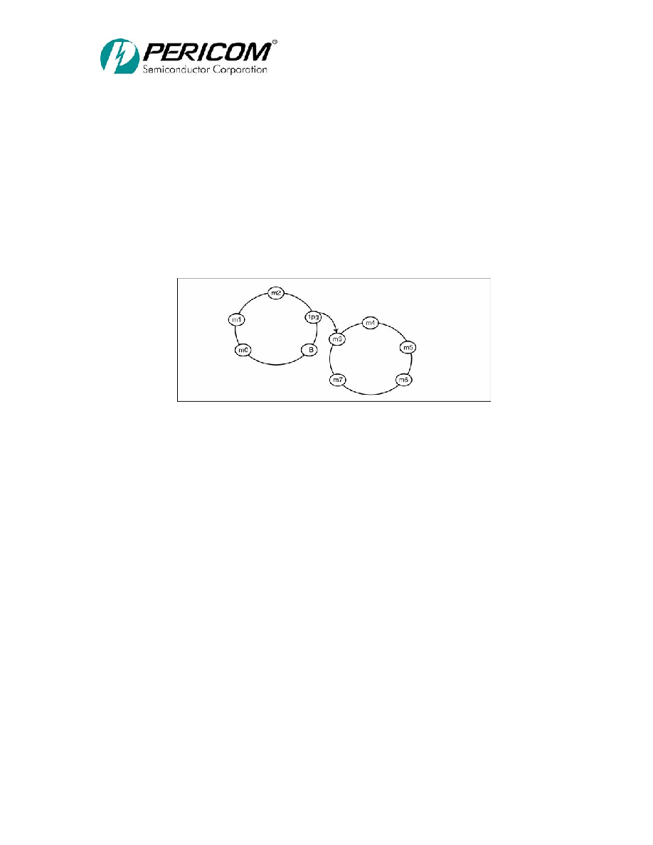
PI7C7300A
3-PORT PCI-TO-PCI BRIDGE
ADVANCE INFORMATION
Page 65 OF 109
09/25/03 Revision 1.09
priority group and a low priority group. The low priority group as a whole represents one
entry in the high priority group; that is, if the high priority group consists of n masters,
then in at least every n+1 transactions the highest priority is assigned to the low priority
group. Priority rotates evenly among the low priority group. Therefore, members of the
high priority group can be serviced n transactions out of n+1, while one member of the
low priority group is serviced once every n+1 transactions. Error! Reference source not
found. shows an example of an internal arbiter where four masters, including
PI7C7300A, are in the high priority group, and five masters are in the low priority group.
Using this example, if all requests are always asserted, the highest priority rotates among
the masters in the following fashion (high priority members are given in italics, low
priority members, in boldface type): B, m0, m1, m2, m3, B, m0, m1, m2, m4, B, m0, m1,
m2, m5, B, m0, m1, m2, m6, B, m0, m1, m2, m7 and so on.
Figure 9-1 SECONDARY ARBITER EXAMPLE
Each bus master, including PI7C7300A, can be configured to be in either the low priority
group or the high priority group by setting the corresponding priority bit in the arbiter-
control register. The arbiter-control register is located at offset 40h. Each master has a
corresponding bit. If the bit is set to 1, the master is assigned to the high priority group. If
the bit is set to 0, the master is assigned to the low priority group. If all the masters are
assigned to one group, the algorithm defaults to a straight rotating priority among all the
masters. After reset, all external masters are assigned to the low priority group, and
PI7C7300A is assigned to the high priority group. PI7C7300A receives highest priority
on the target bus every other transaction, and priority rotates evenly among the other
masters.
Priorities are re-evaluated every time S1_FRAME# or S2_FRAME# is asserted at the
start of each new transaction on the secondary PCI bus. From this point until the time
that the next transaction starts, the arbiter asserts the grant signal corresponding to the
highest priority request that is asserted. If a grant for a particular request is asserted, and
a higher priority request subsequently asserts, the arbiter de-asserts the asserted grant
signal and asserts the grant corresponding to the new higher priority request on the next
PCI clock cycle. When priorities are re-evaluated, the highest priority is assigned to the
next highest priority master relative to the master that initiated the previous transaction.
The master that initiated the last transaction now has the lowest priority in its group.
If PI7C7300A detects that an initiator has failed to assert S1_FRAME# or S2_FRAME#
after 16 cycles of both grant assertion and a secondary idle bus condition, the arbiter de-
asserts the grant. That master does not receive any more grants until it deasserts its
request for at least one PCI clock cycle.
To prevent bus contention, if the secondary PCI bus is idle, the arbiter never asserts one
grant signal in the same PCI cycle in which it deasserts another. It de-asserts one grant

PI7C7300A
3-PORT PCI-TO-PCI BRIDGE
ADVANCE INFORMATION
Page 66 OF 109
09/25/03 Revision 1.09
and asserts the next grant, no earlier than one PCI clock cycle later. If the secondary PCI
bus is busy, that is, either S1_FRAME# (S2_FRAME#) or S1_IRDY# (S2_IRDY#) is
asserted, the arbiter can de-assert one grant and assert another grant during the same PCI
clock cycle.
9.2.2
PREEMPTION
Preemption can be programmed to be either on or off, with the default to on (offset 4Ch,
bit 31=0). Time-to-preempt can be programmed to 8,16, 32, 64, or 128 (default is 32)
clocks.
If the current master occupies the bus and other masters are waiting, the current master
will be preempted by removing its grant (GNT#) after the next master waits for the time-
to-preempt.
9.2.3
SECONDARY BUS ARBITRATION USING AN EXTERNAL
ARBITER
The internal arbiter is disabled when the secondary bus central function control pin,
S_CFN#, is tied high. An external arbiter must then be used.
When S_CFN# is tied high, PI7C7300A, reconfigures four pins (two per port) to be
external request and grant pins. The S1_GNT#[0] and S2_GNT#[0] pins are reconfigured
to be the external request pins because they are output. The S1_REQ#[0] and
S2_REQ#[0] pins are reconfigured to be the external grant pins because they are input.
When an external arbiter is used, PI7C7300A uses the S1_GNT#[0] or S2_GNT#[0] pin
to request the secondary bus. When the reconfigured S1_REQ#[0] and S2_REQ#[0] pin
is asserted low after PI7C7300A has asserted S1_GNT#[0] or S2_GNT#[0]. PI7C7300A
initiates a transaction on the secondary bus one cycle later. If grant is asserted and
PI7C7300A has not asserted the request, PI7C7300A parks AD, CBE and PAR pins by
driving them to valid logic levels.
The unused secondary bus grants outputs, S_GNT#[7:1] and S_GNT#[6:1] are driven
high. The unused secondary bus requests inputs, S1_REQ#[7:1] and S2_REQ#[6:1],
should be pulled high.
9.2.4
BUS PARKING
Bus parking refers to driving the AD[31:0], CBE[3:0]#, and PAR lines to a known value
while the bus is idle. In general, the device implementing the bus arbiter is responsible
for parking the bus or assigning another device to park the bus. A device parks the bus
when the bus is idle, its bus grant is asserted, and the device's request is not asserted. The
AD and CBE signals should be driven first, with the PAR signal driven one cycle later.
PI7C7300A parks the primary bus only when P_GNT# is asserted, P_REQ# is de-
asserted, and the primary PCI bus is idle. When P_GNT# is de-asserted, PI7C7300A 3-
states the P_AD, P_CBE, and P_PAR signals on the next PCI clock cycle. If PI7C7300A
is parking the primary PCI bus and wants to initiate a transaction on that bus, then
PI7C7300A can start the transaction on the next PCI clock cycle by asserting
P_FRAME# if P_GNT# is still asserted.

PI7C7300A
3-PORT PCI-TO-PCI BRIDGE
ADVANCE INFORMATION
Page 67 OF 109
09/25/03 Revision 1.09
If the internal secondary bus arbiter is enabled, the secondary bus is always parked at the
last master that used the PCI bus. That is, PI7C7300A keeps the secondary bus grant
asserted to a particular master until a new secondary bus request comes along. After
reset, PI7C7300A parks the secondary bus at itself until transactions start occurring on
the secondary bus. If the internal arbiter is disabled, PI7C7300A parks the secondary bus
only when the reconfigured grant signal, S_REQ#[0], is asserted and the secondary bus is
idle.
10
COMPACT PCI HOT SWAP
Compact PCI (cPCI) Hot Swap (PICMG 2.1, R1.0) defines a process for installing and
removing PCI boards form a Compact PCI system without powering down the system.
The PI7C7300A is Hot Swap Friendly silicon that supports all the cPCI Hot Swap
Capable features and adds support for Software Connection Control. Being Hot Swap
Friendly, the PI7C7300A supports the following:
!
Compliance with PCI Specification 2.2
!
Tolerates V
CC
from Early Power
!
Asynchronous Reset
!
Tolerates Precharge Voltage
!
I/O Buffers Meet Modified V/I Requirements
!
Limited I/O Pin Leakage at Precharge Voltage
When the PI7C7300A resides on the Compact PCI add-in card, the Primary Bus must be
the bus that is inserted into the Compact PCI system. To perform the Hot Swap function,
the device must be configured according to the CPCI Hot-Swap Specifications. For the
PI7C7300A, the only path for configuration is through the Primary Bus. The bridge may
not be configured through either secondary buses. If the user chooses to use the
secondary buses for insertion, an external register needs to be provided for the Hot Swap
Control Status Register.
11
CLOCKS
This chapter provides information about the clocks.
11.1
PRIMARY CLOCK INPUTS
PI7C7300A implements a primary clock input for the PCI interface. The primary
interface is synchronized to the primary clock input, P_CLK, and the secondary interface
is synchronized to the secondary clock. The secondary clock is derived internally from
the primary clock, P_CLK, through an internal PLL. PI7C7300A operates at a maximum
frequency of 66 MHz.
11.2
SECONDARY CLOCK OUTPUTS
PI7C7300A has 16 secondary clock outputs, S_CLKOUT[15:0] that can be used as clock
inputs for up to fifteen external secondary bus devices. The S_CLKOUT[15:0] outputs

PI7C7300A
3-PORT PCI-TO-PCI BRIDGE
ADVANCE INFORMATION
Page 68 OF 109
09/25/03 Revision 1.09
are derived from P_CLK. The secondary clock edges are delayed from P_CLK edges by
a minimum of 0ns. This is the rule for using secondary clocks:
!
Each secondary clock output is limited to no more than one load.
12
RESET
This chapter describes the primary interface, secondary interface, and chip reset
mechanisms.
12.1
PRIMARY INTERFACE RESET
PI7C7300A has a reset input, P_RESET#. When P_RESET# is asserted, the following
events occur:
!
PI7C7300A immediately 3-states all primary and secondary PCI interface signals.
!
PI7C7300A performs a chip reset.
!
Registers that have default values are reset.
P_RESET# asserting and de-asserting edges can be asynchronous to P_CLK and
S_CLK. PI7C7300A is not accessible during P_RESET#. After P_RESET# is de-
asserted, PI7C7300A remains inaccessible for 2
25
PCI clocks (T
rhfa
, page 128 of the PCI
Local Bus Specification Rev 2.2) before the first configuration transaction can be
accepted.
12.2
SECONDARY INTERFACE RESET
PI7C7300A is responsible for driving the secondary bus reset signals, S1_RESET# and
S2_RESET#. PI7C7300A asserts S1_RESET# or S2_RESET# when any of the
following conditions is met:
!
Signal P_RESET# is asserted. Signal S1_RESET# or S2_RESET# remains
asserted as long as P_RESET# is asserted and does not de-assert until P_RESET# is
de-asserted.
!
The secondary reset bit in the bridge control register is set. Signal S1_RESET#
or S2_RESET# remains asserted until a configuration write operation clears the
secondary reset bit.
!
S1_RESET# or S2_RESET# pin is asserted. When S1_RESET# or S2_RESET# is
asserted, PI7C7300A immediately 3-states all the secondary PCI interface signals
associated with the Secondary S1 or S2 port. The S1_RESET# or S2_RESET# in
asserting and de-asserting edges can be asynchronous to P_CLK.
When S1_RESET# or S2_RESET# is asserted, all secondary PCI interface control
signals, including the secondary grant outputs, are immediately 3-stated. Signals S1_AD,
S1_CBE[3:0]#, S1_PAR (S2_AD, S2_CBE[3:0]#, S2_PAR) are driven low for the

PI7C7300A
3-PORT PCI-TO-PCI BRIDGE
ADVANCE INFORMATION
Page 69 OF 109
09/25/03 Revision 1.09
duration of S1_RESET# (S2_RESET#) assertion. All posted write and delayed
transaction data buffers are reset. Therefore, any transactions residing inside the buffers
at the time of secondary reset are discarded.
When S1_RESET# or S2_RESET# is asserted by means of the secondary reset bit,
PI7C7300A remains accessible during secondary interface reset and continues to respond
to accesses to its configuration space from the primary interface.
13
SUPPORTED COMMANDS
The PCI command set is given below for the primary and secondary interfaces.
13.1
PRIMARY INTERFACE
P_CBE [3:0] #
Command
Action
0000 Interrupt
Acknowledge
Ignore
0001
Special Cycle
Do not claim. Ignore.
0010 I/O
Read
1.
If address is within pass through I/O range, claim and
pass through.
2.
Otherwise, do not pass through and do not claim for
internal access.
0011
I/O Write
Same as I/O Read.
0100 Reserved
-----
0101 Reserved
-----
0110 Memory
Read
1.
If address is within pass through memory range, claim
and pass through.
2.
If address is within pass through memory mapped I/O
range, claim and pass through.
3.
Otherwise, do not pass through and do not claim for
internal access.
0111
Memory Write
Same as Memory Read.
1000 Reserved
-----
1001 Reserved
-----
1010 Configuration
Read
I. Type 0 Configuration Read:
If the bridge's IDSEL line is asserted, perform function
decode and claim if target function is implemented.
Otherwise, ignore. If claimed, permit access to target
function's configuration registers. Do not pass through
under any circumstances.
II. Type 1 Configuration Read:
1.
If the target bus is the bridge's secondary bus: claim
and pass through as a Type 0 Configuration Read.
2.
If the target bus is a subordinate bus that exists behind
the bridge (but not equal to the secondary bus): claim
and pass through as a Type 1 Configuration Read.
3.
Otherwise, ignore.
1011 Configuration
Write
I. Type 0 Configuration Write: same as Configuration
Read.
II. Type 1 Configuration Write (not special cycle
request):
1.
If the target bus is the bridge's secondary bus: claim
and pass through as a Type 0 Configuration Write
2.
If the target bus is a subordinate bus that exists behind
the bridge (but not equal to the secondary bus): claim
and pass through unchanged as a Type 1 Configuration
Write.
3.
Otherwise, ignore.
III. Configuration Write as Special Cycle Request

PI7C7300A
3-PORT PCI-TO-PCI BRIDGE
ADVANCE INFORMATION
Page 70 OF 109
09/25/03 Revision 1.09
P_CBE [3:0] #
Command
Action
(device = 1Fh, function = 7h)
1.
If the target bus is the bridges secondary bus:
claim and pass through as a special cycle.
2.
If the target bus is a subordinate bus that exists
behind the bridge (but not equal to the secondary
bus): claim and pass through unchanged as a type
1 Configuration Write.
3. Otherwise ignore
1100 Memory
Read
Multiple
Same as Memory Read
1101
Dual Address Cycle
Supported
1110
Memory Read Line
Same as Memory Read
1111
Memory Write and
Invalidate
Same as Memory Read
13.2
SECONDARY INTERFACE
S1_CBE [3:0] #
S2_CBE [3:0] #
Command Action
0000 Interrupt
Acknowledge
Ignore
0001
Special Cycle
Do not claim. Ignore.
0010
I/O Read
Same as Primary Interface
0011
I/O Write
Same as I/O Read.
0100 Reserved
-----
0101 Reserved
-----
0110
Memory Read
Same as Primary Interface
0111
Memory Write
Same as Memory Read.
1000 Reserved
-----
1001 Reserved
-----
1010 Configuration
Read
Ignore
1011 Configuration
Write
I. Type 0 Configuration Write: Ignore
II. Type 1 Configuration Write (not special cycle
request):Ignore
III. Configuration Write as Special Cycle Request (device
= 1Fh, function = 7h):
1.
If the target bus is the bridge's primary bus: claim and
pass through as a Special Cycle
2.
If the target bus is neither the primary bus nor is it in
range of buses defined by the bridge's secondary and
subordinate bus registers: claim and pass through
unchanged as a Type 1 Configuration Write.
3.
If the target bus is not the bridge's primary bus, but is
in range of buses defined by the bridge's secondary and
subordinate bus registers: ignore.
1100 Memory
Read
Multiple
Same as Memory Read
1101
Dual Address Cycle
Supported
1110
Memory Read Line
Same as Memory Read
1111
Memory Write and
Invalidate
Same as Memory Read
14
CONFIGURATION REGISTERS
As PI7C7300A supports two secondary interfaces, it has two sets of configuration
registers that are almost identical and accessed through different function numbers. PCI
configuration defines a 64-byte space (configuration header) to define various attributes
of the PCI-to-PCI Bridge as shown below. There are two configuration registers:
Configuration Register 1 and Configuration Register 2 corresponding to Secondary Bus

PI7C7300A
3-PORT PCI-TO-PCI BRIDGE
ADVANCE INFORMATION
Page 71 OF 109
09/25/03 Revision 1.09
1 and Secondary Bus 2 interfaces respectively. The configuration for the Primary
interface is implemented through Configuration Register 1.

PI7C7300A
3-PORT PCI-TO-PCI BRIDGE
ADVANCE INFORMATION
Page 72 OF 109
09/25/03 Revision 1.09
14.1
CONFIGURATION REGISTER 1 AND 2
31-24 23-16 15-8 7-0
Address
Device ID
Vendor ID
00h
Status Command
04h
Class Code
Revision ID
08h
Reserved
Header Type
Primary Latency Timer
Cache Line Size
0Ch
Reserved 10h
Reserved 14h
Secondary Latency
Timer
Subordinate Bus
Number
Secondary Bus
Number
Primary Bus Number
18h
Secondary Status
I/O Limit
I/O Base
1Ch
Memory Limit
Memory Base
20h
Prefetchable Memory Limit
Prefetchable Memory Base
24h
Prefetchable Base Upper 32-bit
28h
Prefetchable Limit Upper 32-bit
2Ch
I/O Limit Upper 16-bit
I/O Base Upper 16-bit
30h
Reserved ECP
Pointer
34h
Reserved 38h
Bridge Control
Reserved
3Ch
Arbiter Control
Diagnostic / Chip Control
40h
Reserved 44h
Upstream Memory Control
Reserved
48h
Hot Swap Switch Time Slot
4Ch
Upstream (S1 or S2 to P) Memory Limit
Upstream (S1 or S2 to P) Memory Base
50h
Upstream (S1 or S2 to P) Memory Base Upper 32-bit
54h
Upstream (S1 or S2 to P) Memory Limit Upper 32-bit
58h
Reserved 5Ch
Reserved 60h
Reserved P_SERR#
Event
Disable
64h
Reserved
Secondary Clock Control
68h
Reserved 6Ch
Reserved 70h
Master Timeout Counter
Port Option
74h
Retry Counter
78h
Sampling Timer
7Ch
Secondary Successful I/O Read Counter
80h
Secondary Successful I/O Write Counter
84h
Secondary Successful Memory Read Counter
88h
Secondary Successful Memory Write Counter
8Ch
Primary Successful I/O Read Counter
90h
Primary Successful I/O Write Counter
94h
Primary Successful Memory Read Counter
98h
Primary Successful Memory Write Counter
9Ch
Reserved A0h-AFh
Chassis Number
Slot Number
Next Pointer
Capability ID
B0h
Reserved B4h-BFh
Hot Swap Control and Status
Next Pointer
Capability ID
C0h
Reserved D0h-FFh
14.1.1
VENDOR ID REGISTER OFFSET 00h
Bit Function
Type Description
15:0
Vendor ID
R/O
Identifies Pericom as vendor of this device. Hardwired as 12D8h.
PI7C7300A
3-PORT PCI-TO-PCI BRIDGE
ADVANCE INFORMATION
Page 73 OF 109
09/25/03 Revision 1.09
14.1.2
DEVICE ID REGISTER OFFSET 00h
Configuration Register 1
Bit Function
Type Description
31:16
Device ID
R/O
Identifies this device as the PI7C7300A. Hardwired as 71E2h.
Configuration Register 2
Bit Function
Type Description
31:16
Device ID
R/O
Identifies this device as the PI7C7300A. Hardwired as 71E3h.
14.1.3
COMMAND REGISTER OFFSET 04h
Bit Function
Type Description
0
I/O Space Enable
R/W
Controls response to I/O access on the primary interface
0: ignore I/O transactions on the primary interface
1: enable response to I/O transactions on the primary interface
Reset to 0
1
Memory Space
Enable
R/W
Controls response to memory accesses on the primary interface
0: ignore memory transactions on the primary interface
1: enable response to memory transactions on the primary interface
Reset to 0
2
Bus Master
Enable
R/W
Controls ability to operate as a bus master on the primary interface
0: do not initiate memory or I/O transactions on the primary
interface and disable response to memory and I/O transactions on
secondary 1 interface
1: enables PI7C7300A to operate as a master on the primary
interfaces for memory and I/O transactions forwarded from the
secondary interface
Reset to 0
3
Special Cycle
Enable
R/O
No special cycles defined.
Bit is defined as read only and returns 0 when read
4
Memory Write
And Invalidate
Enable
R/O
Memory write and invalidate not supported.
Bit is implemented as read only and returns 0 when read (unless
forwarding a transaction for another master)
5
VGA Palette
Snoop Enable
R/W
Controls response to VGA compatible palette accesses
0: ignore VGA palette accesses on the primary
1: enable positive decoding response to VGA palette writes on the
primary interface with I/O address bits AD[9:0] equal to 3C6h,
3C8h, and 3C9h (inclusive of ISA alias; AD[15:10] are not decoded
and may be any value)

PI7C7300A
3-PORT PCI-TO-PCI BRIDGE
ADVANCE INFORMATION
Page 74 OF 109
09/25/03 Revision 1.09
Bit Function
Type Description
6
Parity Error
Response
R/W
Controls response to parity errors
0: PI7C7300A may ignore any parity errors that it detects and
continue normal operation
1: PI7C7300A must take its normal action when a parity error is
detected
Reset to 0
7
Wait Cycle
Control
R/O
Controls the ability to perform address / data stepping
0: disable address/data stepping (affects primary and secondary)
1: enable address/data stepping (affects primary and secondary)
Reset to 0
8 P_SERR#
enable
R/W
Controls the enable for the P_SERR# pin
0: disable the P_SERR# driver
1: enable the P_SERR# driver
Reset to 0
9
Fast Back-to-
Back Enable
R/W
Controls PI7C7300A's ability to generate fast back-to-back
transactions to different devices on the primary interface.
0: no fast back-to-back transactions
1: enable fast back-to-back transactions
Reset to 0
15:10
Reserved
R/O
Returns 000000 when read
14.1.4
STATUS REGISTER OFFSET 04h
Bit Function
Type Description
19:16
Reserved
R/O
Reset to 0
20
Capabilities List
R/O
Set to 1 to enable support for the capability list (offset 34h is the
pointer to the data structure)
Reset to 1
21
66MHz Capable
R/O
Set to 1 to enable 66MHz operation on the primary interface
Reset to 1
22
Reserved
R/O
Reset to 0
23 Fast
Back-to-
Back Capable
R/O
Set to 1 to enable decoding of fast back-to-back transactions on the
primary interface to different targets
Reset to 1
24
Data Parity Error
Detected
R/WC
Set to 1 when P_PERR# is asserted and bit 6 of command register is
set
Reset to 0
26:25 DEVSEL#
timing
R/O
DEVSEL# timing (medium decoding)
00: fast DEVSEL# decoding
01: medium DEVSEL# decoding
10: slow DEVSEL# decoding
11: reserved
Reset to 01

PI7C7300A
3-PORT PCI-TO-PCI BRIDGE
ADVANCE INFORMATION
Page 75 OF 109
09/25/03 Revision 1.09
Bit Function
Type Description
27 Signaled
Target
Abort
R/WC
Set to 1 (by a target device) whenever a target abort cycle occurs
Reset to 0
28 Received
Target
Abort
R/WC
Set to 1 (by a master device) whenever transactions are terminated
with target aborts
Reset to 0
29 Received
Master
Abort
R/WC
Set to 1 (by a master) when transactions are terminated with Master
Abort
Reset to 0
30 Signaled
System
Error
R/WC
Set to 1 when P_SERR# is asserted
Reset to 0
31 Detected
Parity
Error
R/WC
Set to 1 when address or data parity error is detected on the primary
interface
Reset to 0
14.1.5
REVISION ID REGISTER OFFSET 08h
Bit Function
Type Description
7:0
Revision
R/O
Indicates revision number of device. Hardwired to 00h
14.1.6
CLASS CODE REGISTER OFFEST 08h
Bit Function
Type Description
15:8 Programming
Interface
R/O
Read as 0 to indicate no programming interfaces have been defined
for PCI-to-PCI bridges
23:16
Sub-Class Code
R/O
Read as 04h to indicate device is PCI-to-PCI bridge
31:24
Base Class Code
R/O
Read as 06h to indicate device is a bridge device
14.1.7
CACHE LINE SIZE REGISTER OFFSET 0Ch
Bit Function
Type Description
7:0
Cache Line Size
R/W
Designates the cache line size for the system and is used when
terminating memory write and invalidate transactions and when
prefetching memory read transactions.
Only cache line sizes (in units of 4-byte) which are a power of two
are valid (only one bit can be set in this register; only 00h, 01h, 02h,
04h, 08h, and 10h are valid values).
Reset to 0
14.1.8
PRIMARY LATENCY TIMER REGISTER OFFSET 0Ch
Bit Function
Type Description
15:8 Primary
Latency
timer
R/W
This register sets the value for the Master Latency Timer which
starts counting when the master asserts FRAME#.
Reset to 0
PI7C7300A
3-PORT PCI-TO-PCI BRIDGE
ADVANCE INFORMATION
Page 76 OF 109
09/25/03 Revision 1.09
14.1.9
HEADER TYPE REGISTER OFFSET 0Ch
Configuration Register 1
Bit Function
Type Description
23:16
Header Type
R/O
Read as 81h to designate function 0 (multiple function PCI-to-PCI
bridge for secondary bus S1)
Configuration Register 2
Bit Function
Type Description
23:16
Header Type
R/O
Read as 01h to designate function 1 (single function PCI-to-PCI
bridge for secondary bus S2)
14.1.10
PRIMARY BUS NUMBER REGISTER OFFSET 18h
Bit Function
Type Description
7:0 Primary
Bus
Number
R/W
Indicates the number of the PCI bus to which the primary interface
is connected. The value is set in software during configuration.
Reset to 0
14.1.11
SECONDARY (S1 or S2) BUS NUMBER REGISTER OFFSET 18h
Bit Function
Type Description
15:8
Secondary (S1 or
S2) Bus Number
R/W
Indicates the number of the PCI bus to which the secondary
interface (S1 or S2) is connected. The value is set in software
during configuration.
Reset to 0
14.1.12
SUBORDINATE (S1 or S2) BUS NUMBER REGISTER OFFSET
18h
Bit Function
Type Description
23:16 Subordinate
(S1 or S2) Bus
Number
R/W
Indicates the number of the PCI bus with the highest number that is
subordinate to the bridge. The value is set in software during
configuration.
Reset to 0
14.1.13
SECONDARY LATENCY TIMER REGISTER OFFSET 18h
Bit Function
Type Description
31:24 Secondary
Latency Timer
R/W
Designated in units of PCI bus clocks. Latency timer checks for
master accesses on the secondary bus interfaces that remain
unclaimed by any target.
Reset to 0

PI7C7300A
3-PORT PCI-TO-PCI BRIDGE
ADVANCE INFORMATION
Page 77 OF 109
09/25/03 Revision 1.09
14.1.14
I/O BASE REGISTER OFFSET 1Ch
Bit Function
Type Description
3:0
32-bit Indicator
R/O
Read as 01h to indicate 32-bit I/O addressing
7:4
I/O Base Address
[15:12]
R/W
Defines the bottom address of the I/O address range for the bridge
to determine when to forward I/O transactions from one interface to
the other. The upper 4 bits correspond to address bits [15:12] and
are writable. The lower 12 bits corresponding to address bits [11:0]
are assumed to be 0. The upper 16 bits corresponding to address
bits [31:16] are defined in the I/O base address upper 16 bits address
register
Reset to 0
14.1.15
I/O LIMIT REGISTER OFFSET 1Ch
Bit Function
Type Description
11:8
32-bit Indicator
R/O
Read as 01h to indicate 32-bit I/O addressing
15:12
I/O Base Address
[15:12]
R/W
Defines the top address of the I/O address range for the bridge to
determine when to forward I/O transactions from one interface to
the other. The upper 4 bits correspond to address bits [15:12] and
are writable. The lower 12 bits corresponding to address bits [11:0]
are assumed to be FFFh. The upper 16 bits corresponding to
address bits [31:16] are defined in the I/O base address upper 16 bits
address register
Reset to 0
14.1.16
SECONDARY STATUS REGISTER OFFSET 1Ch
Bit Function
Type Description
20:16
Reserved
R/O
Reset to 0
21
66MHz Capable
R/O
Set to 1 to enable 66MHz operation on the secondary (S1 or S2)
interface
Reset to 1
22
Reserved
R/O
Reset to 0
23
Fast Back-to-
Back Capable
R/O
Set to 1 to enable decoding of fast back-to-back transactions on the
secondary (S1 or S2) interface to different targets
Reset to 0
24
Data Parity Error
Detected
R/WC
Set to 1 when S1_PERR# or S2_PERR# is asserted and bit 6 of
command register is set
Reset to 0
26:25
DEVSEL#
timing
R/O
DEVSEL# timing (medium decoding)
00: fast DEVSEL# decoding
01: medium DEVSEL# decoding
10: slow DEVSEL# decoding
11: reserved
Reset to 01
27
Signaled Target
Abort
R/WC
Set to 1 (by a target device) whenever a target abort cycle occurs on
its secondary (S1 or S2) interface
Reset to 0

PI7C7300A
3-PORT PCI-TO-PCI BRIDGE
ADVANCE INFORMATION
Page 78 OF 109
09/25/03 Revision 1.09
Bit Function
Type Description
28
Received Target
Abort
R/WC
Set to 1 (by a master device) whenever transactions on its secondary
(S1 or S2) interface are terminated with target abort
Reset to 0
29
Received Master
Abort
R/WC
Set to 1 (by a master) when transactions on its secondary (S1 or S2)
interface are terminated with Master Abort
Reset to 0
30
Received System
Error
R/WC
Set to 1 when S1_SERR# or S2_SERR# is asserted
Reset to 0
31
Detected Parity
Error
R/WC
Set to 1 when address or data parity error is detected on the
secondary (S1 or S2) interface
Reset to 0
14.1.17
MEMORY BASE REGISTER OFFSET 20h
Bit Function
Type Description
3:0
R/O
Lower four bits of register are read only and return 0.
Reset to 0
15:4 Memory
Base
Address [15:4]
R/W
Defines the bottom address of an address range for the bridge to
determine when to forward memory transactions from one interface
to the other. The upper 12 bits correspond to address bits [31:20]
and are writable. The lower 20 bits corresponding to address bits
[19:0] are assumed to be 0.
Reset to 0
14.1.18
MEMORY LIMIT REGISTER OFFSET 20h
Bit Function
Type Description
19:16
R/O
Lower four bits of register are read only and return 0.
Reset to 0
31:20 Memory
Limit
Address [31:20]
R/W
Defines the top address of an address range for the bridge to
determine when to forward memory transactions from one interface
to the other. The upper 12 bits correspond to address bits [31:20]
and are writable. The lower 20 bits corresponding to address bits
[19:0] are assumed to be FFFFFh.
14.1.19
PREFETCHABLE MEMORY BASE REGISTER OFFSET 24h
Bit Function
Type
Description
3:0
64-bit addressing
R/O
Indicates 64-bit addressing
0000: 32-bit addressing
0001: 64-bit addressing
Reset to 1

PI7C7300A
3-PORT PCI-TO-PCI BRIDGE
ADVANCE INFORMATION
Page 79 OF 109
09/25/03 Revision 1.09
15:4 Prefetchable
Memory Base
Address [31:20]
R/W
Defines the bottom address of an address range for the bridge to
determine when to forward memory read and write transactions from
one interface to the other. The upper 12 bits correspond to address
bits [31:20] and are writable. The lower 20 bits are assumed to be 0.
14.1.20
PREFETCHABLE MEMORY LIMIT REGISTER OFFSET 24h
Bit Function
Type
Description
19:16 64-bit
addressing R/O Indicates 64-bit addressing
0000: 32-bit addressing
0001: 64-bit addressing
Reset to 1
31:20 Prefetchable
Memory Base
Address [31:20]
R/W
Defines the top address of an address range for the bridge to
determine when to forward memory read and write transactions from
one interface to the other. The upper 12 bits correspond to address
bits [31:20] and are writable. The lower 20 bits are assumed to be
FFFFFh.
14.1.21
PREFETCHABLE MEMORY BASE ADDRESS UPPER 32-BITS
REGISTER OFFSET 28h
Bit Function
Type
Description
31:0 Prefetchable
Memory Base
Address, Upper
32-bits [63:32]
R/W
Defines the upper 32-bits of a 64-bit bottom address of an address
range for the bridge to determine when to forward memory read and
write transactions from one interface to the other.
Reset to 0
14.1.22
PREFETCHABLE MEMORY LIMIT ADDRESS UPPER 32-BITS
REGISTER OFFSET 2Ch
Bit Function
Type
Description
31:0 Prefetchable
Memory Limit
Address, Upper
32-bits [63:32]
R/W
Defines the upper 32-bits of a 64-bit top address of an address range
for the bridge to determine when to forward memory read and write
transactions from one interface to the other.
Reset to 0
14.1.23
I/O BASE ADDRESS UPPER 16-BITS REGISTER Offset 30h
Bit Function
Type
Description
15:0 I/O
Base
Address, Upper
16-bits [31:16]
R/W
Defines the upper 16-bits of a 32-bit bottom address of an address
range for the bridge to determine when to forward I/O transactions
from one interface to the other.
Reset to 0

PI7C7300A
3-PORT PCI-TO-PCI BRIDGE
ADVANCE INFORMATION
Page 80 OF 109
09/25/03 Revision 1.09
14.1.24
I/O LIMIT ADDRESS UPPER 16-BITS REGISTER OFFSET 30h
Bit Function
Type
Description
31:0 I/O
Limit
Address, Upper
16-bits [31:16]
R/W
Defines the upper 16-bits of a 32-bit top address of an address range
for the bridge to determine when to forward I/O transactions from
one interface to the other.
Reset to 0
14.1.25
ECP POINTER REGISTER OFFSET 34h
Bit Function
Type
Description
7:0 Enhanced
Capabilities Port
Pointer
R/O
Enhanced capabilities port offset pointer. Read as B0h to indicate
that the first item resides at that configuration offset.
14.1.26
BRIDGE CONTROL REGISTER OFFSET 3Ch
Bit Function
Type
Description
16 Parity
Error
Response
R/W
Controls the bridge's response to parity errors on the secondary
interface.
0: ignore address and data parity errors on the secondary interface
1: enable parity error reporting and detection on the secondary
interface
Reset to 0
17 S1_SERR#
enable
R/W
Controls the forwarding of S1_SERR# or S2_SERR# to the primary
interface.
0: disable the forwarding of S1_SERR# or S2_SERR# to primary
interface
1: enable the forwarding of S1_SERR# or S2_SERR# to primary
interface
Reset to 0
18
ISA enable
R/W
Modifies the bridge's response to ISA I/O addresses, applying only to
those addresses falling within the I/O base and limit address registers
and within the first 64KB or PCI I/O space.
0: forward all I/O addresses in the range defined by the I/O base and
I/O limit registers
1: blocks forwarding of ISA I/O addresses in the range defined by the
I/O base and I/O limit registers that are in the first 64KB of I/O space
that address the last 768 bytes in each 1KB block. Secondary I/O
transactions are forwarded upstream if the address falls within the last
768 bytes in each 1KB block
Reset to 0

PI7C7300A
3-PORT PCI-TO-PCI BRIDGE
ADVANCE INFORMATION
Page 81 OF 109
09/25/03 Revision 1.09
Bit Function
Type
Description
19
VGA enable
R/W
Controls the bridge's response to VGA compatible addresses.
0: does not forward VGA compatible memory and I/O addresses from
primary to secondary
1: forward VGA compatible memory and I/O addresses from primary
to secondary regardless of other settings
Reset to 0
20
Reserved
R/O
Reserved. Returns 0 when read. Reset to 0
21 Master
Abort
Mode
R/W
Control's bridge's behavior responding to master aborts on secondary
interface.
0: does not report master aborts (returns FFFF_FFFFh on reads and
discards data on writes)
1: reports master aborts by signaling target abort if possible by the
assertion of P_SERR# if enabled
Reset to 0
22 Secondary
Interface Reset
R/W
Controls the assertion of S1_RESET# or S2_RESET# signal pin on
the secondary interface
0: does not force the assertion of S1_RESET# or S2_RESET# pin
1: forces the assertion of S1_RESET# or S2_RESET#
Reset to 0
23 Fast
Back-to-
Back Enable
R/W
Controls bridge's ability to generate fast back-to-back transactions to
different devices on the secondary interface.
0: does not allow fast back-to-back transactions
1: enables fast back-to-back transactions
Reset to 0
24
Reserved
R/W
Reserved. Reset to 0
25
Reserved
R/W
Reserved. Reset to 0
26 Master
Timeout
Status
R/WC
This bit is set to 1 when either the primary master timeout counter or
secondary master timeout counter expires.
Reset to 0
27 Discard
Timer
P_SERR# enable
R/WC
This bit Is set to 1 and P_SERR# is asserted when either the primary
discard timer or the secondary S1 or S2 discard timer expire.
Reset to 0
31-28
Reserved
R/O
Reserved. Returns 0 when read. Reset to 0.
14.1.27
DIAGNOSTIC / CHIP CONTROL REGISTER OFFSET 40h
Configuration 1
Bit Function
Type
Description
0
Reserved
R/O
Reserved. Returns 0 when read. Reset to 0
1 Memory
Write
Disconnect
Control
R/W
Controls when the bridge (as a target) disconnects memory write
transactions.
0: memory write disconnects at 4KB aligned address boundary
1: memory write disconnects at cache line aligned address boundary
Reset to 0
3:2 Reserved
R/O Reserved.
Returns 0 when read. Reset to 0.

PI7C7300A
3-PORT PCI-TO-PCI BRIDGE
ADVANCE INFORMATION
Page 82 OF 109
09/25/03 Revision 1.09
Bit Function
Type
Description
4 Memory
Read
Flow-Through
Control
R/W
Controls whether the bridge supports memory read flow-through
0: Enable
1: Disable
Reset to 0
8:5
Reserved
R/O
Reserved. Returns 0 when read. Reset to 0
10:9
Test Mode For
All Counters at P
and S1
R/O
Controls the testability of the bridge's internal counters.
The bits are used for chip test only.
00: all bits are exercised
01: byte 1 is exercised
10: byte 2 is exercised
11: byte 3 is exercised
Reset to 0
15:11
Reserved
R/O
Reserved. Returns 0 when read. Reset to 0.
Configuration 2
Bit Function
Type
Description
0
Reserved
R/O
Reserved. Returns 0 when read. Reset to 0
1 Memory
Write
Disconnect
Control at S2
R/W
Controls when the bridge (as a target) disconnects memory write
transactions.
0: memory write disconnects at 4KB aligned address boundary
1: memory write disconnects at cache line aligned address boundary
Reset to 0
3:2
Reserved
R/O
Reserved. Returns 0 when read. Reset to 0
4 Memory
Read
Flow-through
Control
R/W
Controls whether the bridge supports memory read flow-through
0: Enable
1: Disable
Reset to 0
8:5
Reserved
R/O
Reserved. Returns 0 when read. Reset to 0
10:9
Test Mode For
All Counters at
S2
R/O
Controls the testability of the bridge's internal counters.
The bits are used for chip test only.
00: all bits are exercised
01: byte 1 is exercised
10: byte 2 is exercised
11: byte 3 is exercised
Reset to 0
15:11
Reserved
R/O
Reserved. Returns 0 when read. Reset to 0.

PI7C7300A
3-PORT PCI-TO-PCI BRIDGE
ADVANCE INFORMATION
Page 83 OF 109
09/25/03 Revision 1.09
14.1.28
ARBITER CONTROL REGISTER OFFSET 40h
Bit Function
Type
Description
23:16
Arbiter Control
R/W
Each bit controls whether a secondary bus master is assigned to the
high priority group or the low priority group.
Bits [23:16] correspond to request inputs S1_REQ[7:0] or
S2_REQ[6:0]
0: low priority
1: high priority
Reset to 0
24
Reserved
R/O
Reserved. Returns 0 when read. Reset to 0
25 Priority
of
Secondary
Interface
R/W
Controls whether the S1 or S2 interface of the bridge is in the high
priority group or the low priority group.
0: low priority
1: high priority
Reset to 1
26 Arbiter
Park
Function
R/W
Controls the arbiter's park function.
0: park to last master
1: park to bridge port S1 or S2
Reset to 0
31:27
Reserved
R/O
Reserved. Returns 0 when read. Reset to 0.
14.1.29
UPSTREAM MEMORY CONTROL REGISTER OFFSET 48h
Bit Function
Type
Description
16
Upstream (S1 or
S2 to P) Memory
Base and Limit
Enable
R/W
0: Upstream memory is the entire range except the down stream
memory channel
1: Upstream memory is confined to upstream Memory Base and Limit
(See offset 50
th
and 54
th
for upstream memory range)
Reset to 0
17
Upstream (S1 or
S2 to P) Memory
Prefetchable
Enable
R/W
0: Upstream memory is prefetchable at Primary
1: Upstream memory is not prefetchable at Primary
Reset to 0
31:18
Reserved
R/O
Reserved. Returns 0 when read. Reset to 0
14.1.30
HOT SWAP SWITCH TIME SLOT REGISTER OFFSET 4Ch
Bit Function
Type
Description
27:0
Hot Swap Time
Slot
R/W
Hot Swap time slot (15K PCI clocks)
Reset to 0003A98h

PI7C7300A
3-PORT PCI-TO-PCI BRIDGE
ADVANCE INFORMATION
Page 84 OF 109
09/25/03 Revision 1.09
Bit Function
Type
Description
30:28
Secondary Bus
Master
Preemption
Control
R/W
Sets the number of clocks for time-to-preempt after another master
request.
000: 32 clocks
001: 8 clocks
010: 16 clocks
011: 64 clocks
100: 128 clocks
Reset to 000
31 Preemption R/W
Sets preemption.
0: preemption ON
1: preemption OFF
Reset to 0
14.1.31
UPSTREAM (S1 or S2 to P) MEMORY BASE REGISTER
OFFSET 50h
Bit Function
Type
Description
3:0
64 bit addressing
R/O
0: 32 bit addressing
1: 64 bit addressing
Reset to 1
15:4
Upstream
Memory Base
Address
R/W
Controls upstream memory base address.
Reset to 00000000h
14.1.32
UPSTREAM (S1 or S2 to P) MEMORY LIMIT REGISTER
OFFSET 50h
Bit Function
Type
Description
19:16
64 bit addressing
R/O
0: 32 bit addressing
1: 64 bit addressing
Reset to 1
31:20
Upstream
Memory Limit
Address
R/W
Controls upstream memory limit address.
Reset to 000FFFFFh
14.1.33
UPSTREAM (S1 or S2 to P) MEMORY BASE UPPER 32-BITS
REGISTER OFFSET 54h
Bit Function
Type
Description
31:0
Upstream
Memory Base
Address
R/W
Defines bits [63:32] of the upstream memory base
Reset to 0

PI7C7300A
3-PORT PCI-TO-PCI BRIDGE
ADVANCE INFORMATION
Page 85 OF 109
09/25/03 Revision 1.09
14.1.34
UPSTREAM (S1 or S2 to P) MEMORY LIMIT UPPER 32 BITS
REGISTER OFFSET 58h
Bit Function
Type
Description
31:0
Upstream
Memory Limit
Address
R/W
Defines bits [63:32] of the upstream memory limit
Reset to 0
14.1.35
P_SERR# EVENT DISABLE REGISTER OFFSET 64h
Bit Function
Type
Description
0
Reserved
R/O
Reserved. Returns 0 when read. Reset to 0
1
Posted Write
Parity Error
R/W
Controls PI7C7300A's ability to assert P_SERR# when it is unable to
transfer any read data from the target after 2
24
attempts.
0: P_SERR# is asserted if this event occurs and the SERR# enable bit
in the command register is set.
1: P_SERR# is not assert if this event occurs.
Reset to 0
2
Posted Write
Non-Delivery
R/W
Controls PI7C7300A's ability to assert P_SERR# when it is unable to
transfer delayed write data after 2
24
attempts.
0: P_SERR# is asserted if this event occurs and the SERR# enable bit
in the command register is set
1: P_SERR# is not asserted if this event occurs
Reset to 0
3
Target Abort
During Posted
Write
R/W
Controls PI7C7300A's ability to assert P_SERR# when it receives a
target abort when attempting to deliver posted write data.
0: P_SERR# is asserted if this event occurs and the SERR# enable bit
in the command register is set
1: P_SERR# is not asserted if this event occurs
Reset to 0
4
Master Abort On
Posted Write
R/W
Controls PI7C7300A's ability to assert P_SERR# when it receives a
master abort when attempting to deliver posted write data.
0: P_SERR# is asserted if this event occurs and the SERR# enable bit
in the command register is set
1: P_SERR# is not asserted if this event occurs
Reset to 0
5
Delayed Write
Non-Delivery
R/W
Controls PI7C7300A's ability to assert P_SERR# when it is unable to
transfer delayed write data after 2
24
attempts.
0: P_SERR# is asserted if this event occurs and the SERR# enable bit
in the command register is set
1: P_SERR# is not asserted if this event occurs
Reset to 0

PI7C7300A
3-PORT PCI-TO-PCI BRIDGE
ADVANCE INFORMATION
Page 86 OF 109
09/25/03 Revision 1.09
Bit Function
Type
Description
6
Delayed Read
No Data From
Target
R/W
Controls PI7C7300A's ability to assert P_SERR# when it is unable to
transfer any read data from the target after 2
24
attempts.
0: P_SERR# is asserted if this event occurs and the SERR# enable bit
in the command register is set
1: P_SERR# is not asserted if this event occurs
Reset to 0
7
Reserved
R/O
Reserved. Returns 0 when read. Reset to 0
14.1.36
SECONDARY CLOCK CONTROL REGISTER OFFSET 68h
Configuration Register 1
Bit Function
Type
Description
1:0
Clock 0 disable
R/W
If either bit is 0, then S1_CLKOUT [0] is enabled.
If both bits are 1, the S1_CLKOUT [0] is disabled.
3:2
Clock 1 disable
R/W
If either bit is 0, then S1_CLKOUT [1] is enabled.
If both bits are 1, the S1_CLKOUT [1] is disabled.
5:4
Clock 2 disable
R/W
If either bit is 0, then S1_CLKOUT [2] is enabled.
If both bits are 1, the S1_CLKOUT [2] is disabled.
7:6
Clock 3 disable
R/W
If either bit is 0, then S1_CLKOUT [3] is enabled.
If both bits are 1, the S1_CLKOUT [3] is disabled.
9:8
Clock 4 disable
R/W
If either bit is 0, then S1_CLKOUT [4] is enabled.
If both bits are 1, the S1_CLKOUT [4] is disabled.
11:10
Clock 5 disable
R/W
If either bit is 0, then S1_CLKOUT [5] is enabled.
If both bits are 1, the S1_CLKOUT [5] is disabled.
13:12
Clock 6 disable
R/W
If either bit is 0, then S1_CLKOUT [6] is enabled.
If both bits are 1, the S1_CLKOUT [6] is disabled.
15:14
Clock 7 disable
R/W
If either bit is 0, then S1_CLKOUT [7] is enabled.
If both bits are 1, the S1_CLKOUT [7] is disabled.
Configuration Register 2
Bit Function
Type
Description
1:0
Clock 0 disable
R/W
If either bit is 0, then S2_CLKOUT [0] is enabled.
If both bits are 1, the S2_CLKOUT [0] is disabled.
3:2
Clock 1 disable
R/W
If either bit is 0, then S2_CLKOUT [1] is enabled.
If both bits are 1, the S2_CLKOUT [1] is disabled.
5:4
Clock 2 disable
R/W
If either bit is 0, then S2_CLKOUT [2] is enabled.
If both bits are 1, the S2_CLKOUT [2] is disabled.
7:6
Clock 3 disable
R/W
If either bit is 0, then S2_CLKOUT [3] is enabled.
If both bits are 1, the S2_CLKOUT [3] is disabled.
9:8
Clock 4 disable
R/W
If either bit is 0, then S2_CLKOUT [4] is enabled.
If both bits are 1, the S2_CLKOUT [4] is disabled.
11:10
Clock 5 disable
R/W
If either bit is 0, then S2_CLKOUT [5] is enabled.
If both bits are 1, the S2_CLKOUT [5] is disabled.
13:12
Clock 6 disable
R/W
If either bit is 0, then S2_CLKOUT [6] is enabled.
If both bits are 1, the S2_CLKOUT [6] is disabled.
15:14
Clock 7 disable
R/W
If either bit is 0, then S2_CLKOUT [7] is enabled.
If both bits are 1, the S2_CLKOUT [7] is disabled.
14.1.37
PORT OPTION REGISTER OFFSET 74h
Bit Function
Type
Description
0
Reserved
R/O
Reserved. Returns 0 when read. Reset to 0.

PI7C7300A
3-PORT PCI-TO-PCI BRIDGE
ADVANCE INFORMATION
Page 87 OF 109
09/25/03 Revision 1.09
Bit Function
Type
Description
1
Primary MEMR
Command Alias
Enable
R/W
Controls PI7C7300A's detection mechanism for matching memory
read retry cycles from the initiator on the primary interface
0: exact matching for non-posted memory write retry cycles from
initiator on the primary interface
1: alias MEMRL or MEMRM to MEMR for memory read retry
cycles from the initiator on the primary interface
Reset to 0
2
Primary MEMW
Command Alias
Enable
R/W
Controls PI7C7300A's detection mechanism for matching non-posted
memory write retry cycles from the initiator on the primary interface
0: exact matching for non-posted memory write retry cycles from
initiator on the primary interface
1: alias MEMWI to MEMW for non-posted memory write retry
cycles from initiator on the primary interface
Reset to 0
3
Secondary
MEMR
Command Alias
Enable
R/W
Controls PI7C7300A's detection mechanism for matching memory
read retry cycles from the initiator on S1
0: exact matching for memory read retry cycles from initiator on the
S1 or S2 interface
1: alias MEMRL or MEMRM to MEMR for memory read retry
cycles from initiator on the S1 or S2 interface
Reset to 0
4
Secondary
MEMW
Command Alias
Enable
R/W
Controls PI7C7300A's detection mechanism for matching non-posted
memory write retry cycles from the initiator on the primary interface
0: exact matching for non-posted memory write retry cycles from
initiator on the S1 or S2 interface
1: alias MEMWI to MEMW for non-posted memory write retry
cycles from initiator on the S1 or S2 interface
Reset to 0
8:5
Reserved
R/O
Reserved. Returns 0 when read. Reset to 0.
9
Enable Long
Request
R/W
Controls PI7C7300A's ability to enable long requests for lock cycles
0: normal lock operation
1: enable long request for lock cycle
Reset to 0
10
Enable
Secondary To
Hold Request
Longer
R/W
Control's PI7C7300A's ability to enable S1 or S2 to hold requests
longer.
0: internal S1 or S2 master will release REQ_L after FRAME_L
assertion
1: internal S1 or S2 master will hold REQ_L until there is no
transactions pending in FIFO or until terminated by target
Reset to 1
PI7C7300A
3-PORT PCI-TO-PCI BRIDGE
ADVANCE INFORMATION
Page 88 OF 109
09/25/03 Revision 1.09
Bit Function
Type
Description
11
Enable Primary
To Hold Request
Longer
R/W
Control's PI7C7300A's ability to hold requests longer at the Primary
Port.
0: internal Primary master will release REQ_L after FRAME_L
assertion
1: internal Primary master will hold REQ_L until there is no
transactions pending in FIFO or until terminated by target
Reset to 1
15:12
Reserved
R/O
Reserved. Returns 0 when read. Reset to 0.
14.1.38
MASTER TIMEOUT COUNTER REGISTER OFFSET 74h
Bit Function
Type
Description
31:16 Master
Timeout R/W
Holds the maximum number of PCI clocks that PI7C7300A will wait
for initiator to retry the same cycle before reporting timeout. Master
timeout occurs after 2
15
PCI clocks.
Default is 8000h.
14.1.39
RETRY COUNTER REGISTER OFFSET 78h
Bit Function
Type
Description
31:0 Retry
Counter R/W
Holds the maximum number of attempts that PI7C7300A will try
before reporting retry timeout. Retry count set at 2
24
PCI clocks.
Default is 0100 0000h.
14.1.40
SAMPLING TIMER REGISTER OFFSET 7Ch
Bit Function
Type
Description
31:0 Sampling
Timer R/W
Sets the duration (in PCI clocks) during which PI7C7300A will
record the number of successful transactions for performance
evaluation. The recording will start right after this register is
programmed and will be cleared after the timer expires. Maximum
period is 128 seconds at 33MHz.
Reset to 0.
14.1.41
SECONDARY SUCCESSFUL I/O READ COUNTER REGISTER
OFFSET 80h
Bit Function
Type
Description
31:0
Successful I/O
Read Counts on
S1 or S2
R/W
Stores the successful I/O read count on S1 or S2 and is updated when
the sampling timer is active.
Reset to 0
PI7C7300A
3-PORT PCI-TO-PCI BRIDGE
ADVANCE INFORMATION
Page 89 OF 109
09/25/03 Revision 1.09
14.1.42
SECONDARY SUCCESSFUL I/O WRITE COUNTER REGISTER
OFFSET 84h
Bit Function
Type
Description
31:0
Successful I/O
Write Counts on
S1 or S2
R/W
Stores the successful I/O write count on S1 or S2 and is updated
when the sampling timer is active.
Reset to 0
14.1.43
SECONDARY SUCCESSFUL MEMORY READ COUNTER
REGISTER Offset 88h
Bit Function
Type
Description
31:0
Successful
Memory Read
Counts on S1 or
S2
R/W
Stores the successful memory read count on S1 or S2 and is updated
when the sampling timer is active.
Reset to 0
14.1.44
SECONDARY SUCCESSFUL MEMORY WRITE COUNTER
REGISTER OFFSET 8Ch
Bit Function
Type
Description
31:0
Successful
Memory Write
Counts on S1 or
S2
R/W
Stores the successful memory write count on S1 or S2 and is updated
when the sampling timer is active.
Reset to 0
14.1.45
PRIMARY SUCCESSFUL I/O READ COUNTER REGISTER
OFFSET 90h
Bit Function
Type
Description
31:0
Successful I/O
Read Counts on
Primary
R/W
Stores the successful I/O read count on Primary and is updated when
the sampling timer is active.
Reset to 0
14.1.46
PRIMARY SUCCESSFUL I/O WRITE COUNTER REGISTER
OFFSET 94h
Bit Function
Type
Description
31:0
Successful I/O
Write Counts on
Primary
R/W
Stores the successful I/O write count on Primary and is updated when
the sampling timer is active.
Reset to 0

PI7C7300A
3-PORT PCI-TO-PCI BRIDGE
ADVANCE INFORMATION
Page 90 OF 109
09/25/03 Revision 1.09
14.1.47
PRIMARY SUCCESSFUL MEMORY READ COUNTER
REGISTER OFFSET 98h
Bit Function
Type
Description
31:0
Successful
Memory Read
Counts on
Primary
R/W
Stores the successful memory read count on Primary and is updated
when the sampling timer is active.
Reset to 0
14.1.48
PRIMARY SUCCESSFUL MEMORY WRITE COUNTER
REGISTER OFFSET 9Ch
Bit Function
Type
Description
31:0
Successful
Memory Write
Counts on
Primary
R/W
Stores the successful memory write count on Primary and is updated
when the sampling timer is active.
Reset to 0
14.1.49
CAPABILITY ID REGISTER OFFSET B0h
Bit Function
Type
Description
7:0 Capability
ID R/O
Capability ID for slot identification
00h: Reserved
01h: PCI Power Management (PCIPM)
02h: Accelerated Graphics Port (AGP)
03h: Vital Product Data (VPD)
04h: Slot Identification (SI)
05h: Message Signaled Interrupts (MSI)
06h: Compact PCI Hot Swap (CHS)
07h 255h: Reserved
Reset to 04h
14.1.50
NEXT POINTER REGISTER OFFSET B0h
Bit Function
Type
Description
15:8 Next
Pointer
R/O
Reset to 1100 0000: next pointer (C0h if HS_EN is 1)
0000 0000: next pointer (00h if HS_EN is 0)
PI7C7300A
3-PORT PCI-TO-PCI BRIDGE
ADVANCE INFORMATION
Page 91 OF 109
09/25/03 Revision 1.09
14.1.51
SLOT NUMBER REGISTER OFFSET B0h
Bit Function
Type
Description
20:16
Expansion Slot
Number
R/W
Determines expansion slot number
Reset to 0
21
First in Chassis
R/W
First in chassis
Reset to 0
23:22
Reserved
R/O
Reserved. Returns 0 when read. Reset to 0.
14.1.52
CHASSIS NUMBER REGISTER OFFSET B0h
Bit Function
Type
Description
31:24
Chassis Number
Register
R/W
Chassis number register.
Reset to 0
14.1.53
CAPABILITY ID REGISTER OFFSET C0h
Bit Function
Type
Description
7:0
Capability ID for
Hot Swap
R/O
Capability ID for Hot Swap
00h: Reserved
01h: PCI Power Management (PCIPM)
02h: Accelerated Graphics Port (AGP)
03h: Vital Product Data (VPD)
04h: Slot Identification (SI)
05h: Message Signaled Interrupts (MSI)
06h: Compact PCI Hot Swap (CHS)
07h 255h: Reserved
Reset to 06h
14.1.54
NEXT POINTER REGISTER OFFSET C0h
Bit Function
Type
Description
15:8
Next Pointer
R/O
00: End of pointer (00h).
14.1.55
HOT SWAP CONTROL AND STATUS REGISTER OFFSET C0h
Bit Function
Type
Description
16
Not Available
R/O
Not used. Returns 0 when read. Reset to 0
17
ENUM Signal
Mask
R/W
0: Mask ENUM# signal
1: Enable ENUM# signal
18
Not Available
R/O
Not used. Returns 0 when read. Reset to 0

PI7C7300A
3-PORT PCI-TO-PCI BRIDGE
ADVANCE INFORMATION
Page 92 OF 109
09/25/03 Revision 1.09
Bit Function
Type
Description
19 LED
ON/OFF R/W
LOO signal (LED on/off)
0: LED on
1: LED off
Reset to 0
21:20
Not Available
R/O
Not Used. Returns 0 when read. Reset to 0
22
ENUM# Status
Extraction
R/W
0: ENUM# asserted
1: ENUM# not asserted
Reset to 0
23
ENUM# Status
Insertion
R/W
0: ENUM# asserted
1: ENUM# not asserted
Reset to 0
31:24
Reserved
R/O
Reserved. Returns 0 when read. Reset to 0
15
BRIDGE BEHAVIOR
A PCI cycle is initiated by asserting the FRAME# signal. In a bridge, there are a number
of possibilities. Those possibilities are summarized in the table below:
15.1
BRIDGE ACTIONS FOR VARIOUS CYCLE TYPES
Initiator Target Response
Master on Primary
Target on Primary
PI7C7300A does not respond. It detects
this situation by decoding the address as
well as monitoring the P_DEVSEL# for
other fast and medium devices on the
Primary Port.
Master on Primary
Target on Secondary
PI7C7300A asserts P_DEVSEL#,
terminates the cycle normally if it is able
to be posted, otherwise return with a retry.
It then passes the cycle to the appropriate
port. When the cycle is complete on the
target port, it will wait for the initiator to
repeat the same cycle and end with normal
termination.
Master on Primary
Target not on Primary nor
Secondary Port
PI7C7300A does not respond and the
cycle will terminate as master abort.
Master on Secondary
Target on the same
Secondary Port
PI7C7300A does not respond.
Master on Secondary
Target on Primary or the
other Secondary Port
PI7C7300A asserts S1_DEVSEL# or
S2_DEVSEL#, terminates the cycle
normally if it is able to be posted,
otherwise returns with a retry. It then
passes the cycle to the appropriate port.
When cycle is complete on the target port,
it will wait for the initiator to repeat the
same cycle and end with normal
termination.
Master on Secondary
Target not on Primary nor
the other Secondary Port
PI7C7300A does not respond.
PI7C7300A
3-PORT PCI-TO-PCI BRIDGE
ADVANCE INFORMATION
Page 93 OF 109
09/25/03 Revision 1.09
15.2
TRANSACTION ORDERING
To maintain data coherency and consistency, PI7C7300A complies with the ordering
rules put forth in the PCI Local Bus Specification, Rev 2.2. The following table
summarizes the ordering relationship of all the transactions through the bridge.
PMW - Posted write (either memory write or memory write & invalidate)
DRR - Delayed read request (all memory read, I/O read & configuration read)
DWR - Delayed write request (I/O write & configuration write, memory write to
certain location)
DRC - Delayed read completion (all memory read, I/O read & configuration read)
DWC - Delayed write completion (I/O write & configuration write, memory write
to ccertain location
Cycle type shown on each row is the subsequent cycle after the previous shown on the
column.
Can Row Pass Column?
PMW
Column 1
DRR
Column 2
DWR
Column 3
DRC
Column 4
DWC
Column 5
PMW (Row 1)
No
Yes
Yes
Yes
Yes
DRR (Row 2)
No
No
No
Yes
Yes
DWR (Row 3)
No
No
No
Yes
Yes
DRC (Row 4)
No
Yes
Yes
No
No
DWC (Row 5)
Yes
Yes
Yes
No
No
In Row 1 Column 1, PMW cannot pass the previous PMW and that means they must
complete on the target bus in the order in which they were received in the initiator bus.
In Row 2 Column1,DRR cannot pass the previous PMW and that means the previous
PMW heading to the same direction must be completed before the DRR can be attempted
on the target bus.
In Row 1 Column 2, PMW can pass the previous DRR as long as the DRR reaches the
head of the delayed transaction queue.
15.3
ABNORMAL TERMINATION (INITIATED BY BRIDGE
MASTER)
15.3.1
MASTER ABORT
Master abort indicates that when PI7C7300A acts as a master and receives no response
(i.e., no target asserts DEVSEL# or S1_DEVSEL# or S2_DEVSEL#) from a target, the
bridge deasserts FRAME# and then deasserts IRDY#.
15.3.2
PARITY AND ERROR REPORTING
Parity must be checked for all addresses and write data. Parity is defined on the P_PAR,
S1_PAR, and S2_PAR signals. Parity should be even (i. e. an even number of`1's) across
AD, CBE, and PAR. Parity information on PAR is valid the cycle after AD and CBE are

PI7C7300A
3-PORT PCI-TO-PCI BRIDGE
ADVANCE INFORMATION
Page 94 OF 109
09/25/03 Revision 1.09
valid. For reads, even parity must be generated using the initiators CBE signals combined
with the read data. Again, the PAR signal corresponds to read data from the previous
data phase cycle.
15.3.3
REPORTING PARITY ERRORS
For all address phases, if a parity error is detected, the error should be reported on the
P_SERR# signal by asserting P_SERR# for one cycle and then 3-stating two cycles after
the bad address. P_SERR# can only be asserted if bit 6 and 8 in the Command Register
are both set to 1. For write data phases, a parity error should be reported by asserting the
P_PERR# signal two cycles after the data phase and should remain asserted for one cycle
when bit 6 in the Command register is set to a 1. The target reports any type of data
parity errors during write cycles, while the master reports data parity errors during read
cycles.
Detection of an address parity error will cause the PCI-to-PCI Bridge target to not claim
the bus (P_DEVSEL# remains inactive) and the cycle will then terminate with a Master
Abort. When the bridge is acting as master, a data parity error during a read cycle results
in the bridge master initiating a Master Abort.
15.3.4
SECONDARY IDSEL MAPPING
When PI7C7300A detects a Type 1 configuration transaction for a device connected to
the secondary, it translates the Type 1 transaction to Type 0 transaction on the
downstream interface. Type 1 configuration format uses a 5-bit field at P_AD[15:11] as a
device number. This is translated to S1_AD[31:16] or S2_AD[31:16] by PI7C7300A.
16
IEEE 1149.1 COMPATIBLE JTAG CONTROLLER
An IEEE 1149.1 compatible Test Access Port (TAP) controller and associated TAP pins
are provided to support boundary scan in PI7C7300A for board-level continuity test and
diagnostics. The TAP pins assigned are TCK, TDI, TDO, TMS and TRST#. All digital
input, output, input/output pins are tested except TAP pins and clock pin.
The IEEE 1149.1 Test Logic consists of a TAP controller, an instruction register, and
a group of test data registers including Bypass, Device Identification and Boundary Scan
registers. The TAP controller is a synchronous 16-state machine driven by the Test Clock
(TCK) and the Test Mode Select (TMS) pins. An independent power on reset circuit is
provided to ensure the machine is in TEST_LOGIC_RESET state at power-up. The
JTAG signal lines are not active when the PCI resource is operating PCI bus cycles.
PI7C7300A implements 3 basic instructions: BYPASS, SAMPLE/PRELOAD, and
EXTEST.
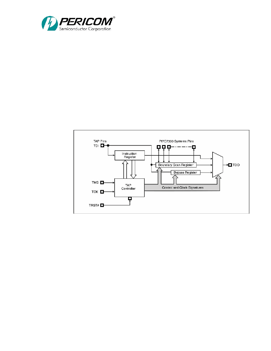
PI7C7300A
3-PORT PCI-TO-PCI BRIDGE
ADVANCE INFORMATION
Page 95 OF 109
09/25/03 Revision 1.09
16.1
BOUNDARY SCAN ARCHITECTURE
Boundary-scan test logic consists of a boundary-scan register and support logic. These
are accessed through a Test Access Port (TAP). The TAP provides a simple serial
interface that allows all processor signal pins to be driven and/or sampled, thereby
providing direct control and monitoring of processor pins at the system level.
This mode of operation is valuable for design debugging and fault diagnosis since it
permits examination of connections not normally accessible to the test system. The
following subsections describe the boundary-scan test logic elements: TAP pins,
instruction register, test data registers and TAP controller. Error! Reference source not
found. illustrates how these pieces fit together to form the JTAG unit.
Figure 16-1 TEST ACCESS PORT BLOCK DIAGRAM
16.1.1
TAP PINS
The PI7C7300A's TAP pins form a serial port composed of four input connections
(TMS, TCK, TRST# and TDI) and one output connection (TDO). These pins are
described in Table 16-1. The TAP pins provide access to the instruction register and the
test data registers.
16.1.2
INSTRUCTION REGISTER
The Instruction Register (IR) holds instruction codes. These codes are shifted in through
the Test Data Input (TDI) pin. The instruction codes are used to select the specific test
operation to be performed and the test data register to be accessed.
The instruction register is a parallel-loadable, master/slave-configured 4-bit wide, serial-
shift register with latched outputs. Data is shifted into and out of the IR serially through
the TDI pin clocked by the rising edge of TCK. The shifted-in instruction becomes active
upon latching from the master stage to the slave stage. At that time the IR outputs along
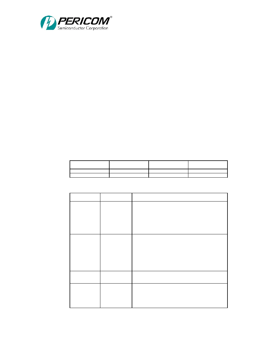
PI7C7300A
3-PORT PCI-TO-PCI BRIDGE
ADVANCE INFORMATION
Page 96 OF 109
09/25/03 Revision 1.09
with the TAP finite state machine outputs are decoded to select and control the test data
register selected by that instruction. Upon latching, all actions caused by any previous
instructions terminate.
The instruction determines the test to be performed, the test data register to be accessed,
or both. The IR is two bits wide. When the IR is selected, the most significant bit is
connected to TDI, and the least significant bit is connected to TDO. The value presented
on the TDI pin is shifted into the IR on each rising edge of TCK. The TAP controller
captures fixed parallel data (1101 binary). When a new instruction is shifted in through
TDI, the value 1101(binary) is always shifted out through TDO, least significant bit first.
This helps identify instructions in a long chain of serial data from several devices.
Upon activation of the TRST# reset pin, the latched instruction asynchronously changes
to the id code instruction. When the TAP controller moves into the test state other than
by reset activation, the opcode changes as TDI shifts, and becomes active on the falling
edge of TCK.
16.2
BOUNDARY-SCAN INSTRUCTION SET
The PI7C7300A supports three mandatory boundary-scan instructions (bypass,
sample/preload and extest). The table shown below lists the PI7C7300A's boundary-scan
instruction codes. The "reserved" code should not be used.
Instruction Code
(binary)
Instruction Name
Instruction Code
(binary)
Instruction Name
0000 EXTEST
0101 Reserved
0001 SAMPLE/PRELOAD
1111 Bypass
Table 16-1 TAP PINS
Instruction /
Requisite
Opcode (binary)
Description
Extest
IEEE 1149.1
Required
0000
Extest initiates testing of external circuitry, typically board-level
interconnects and off chip circuitry. Extest connects the
boundary-scan register between TDI and TDO. When Extest is
selected, all output signal pin values are driven by values shifted
into the boundary-scan register and may change only of the
falling edge of TCK. Also, when extest is selected, all system
input pin states must be loaded into the boundary-scan register on
the rising-edge of TCK.
Sample/preload
IEEE 1149.1
Required
0001
Sample/preload performs two functions:
1. A snapshot of the sample instruction is captured on the rising
edge of TCK without interfering with normal operation. The
instruction causes boundary-scan register cells associated with
outputs to sample the value being driven.
2. On the falling edge of TCK, the data held in the boundary-scan
cells is transferred to the slave register cells. Typically, the
slave latched data is applied to the system outputs via the
extest instruction.
Idcode
IEEE 1149.1
Required
0101 Reserved
Bypass
IEEE 1149.1
Required
1111
Bypass instruction selects the one-bit bypass register between
TDI and TDO pins. 0 (binary) is the only instruction that
accesses the bypass register. While this instruction is in effect,
all other test data registers have no effect on system operation.
Test data registers with both test and system functionality
perform their system functions when this instruction is selected.

PI7C7300A
3-PORT PCI-TO-PCI BRIDGE
ADVANCE INFORMATION
Page 97 OF 109
09/25/03 Revision 1.09
16.3
TAP TEST DATA REGISTERS
The PI7C7300A contains two test data registers (bypass and boundary-scan). Each test
data register selected by the TAP controller is connected serially between TDI and TDO.
TDI is connected to the test data register's most significant bit. TDO is connected to the
least significant bit. Data is shifted one bit position within the register towards TDO on
each rising edge of TCK. While any register is selected, data is transferred from TDI to
TDO without inversion. The following sections describe each of the test data registers.
16.4
BYPASS REGISTER
The required bypass register, a one-bit shift register, provides the shortest path between
TDI and TDO when a bypass instruction is in effect. This allows rapid movement of test
data to and from other components on the board. This path can be selected when no test
operation is being performed on the PI7C7300A.
16.5
BOUNDARY-SCAN REGISTER
The boundary-scan register contains a cell for each pin as well as control cells for I/O
and the high-impedance pin.
Table 16-2 shows the bit order of the PI7C7300A boundary-scan register. All table cells
that contain "Control" select the direction of bi-directional pins or high-impedance
output pins. When a "0" is loaded into the control cell, the associated pin(s) are high-
impedance or selected as input.
The boundary-scan register is a required set of serial-shiftable register cells, configured
in master/slave stages and connected between each of the PI7C7300A's pins and on-chip
system logic. The VDD, GND, PLL, AGND, AVDD and JTAG pins are NOT in the
boundary-scan chain.
The boundary-scan register cells are dedicated logic and do not have any system
function. Data may be loaded into the boundary-scan register master cells from the
device input pins and output pin-drivers in parallel by the mandatory sample/preload and
extest instructions. Parallel loading takes place on the rising edge of TCK.
Data may be scanned into the boundary-scan register serially via the TDI serial input pin,
clocked by the rising edge of TCK. When the required data has been loaded into the
master-cell stages, it can be driven into the system logic at input pins or onto the output
pins on the falling edge of TCK state. Data may also be shifted out of the boundary-scan
register by means of the TDO serial output pin at the falling edge of TCK.
16.6
TAP CONTROLLER
The TAP (Test Access Port) controller is a 4-state synchronous finite state machine that
controls the sequence of test logic operations. The TAP can be controlled via a bus
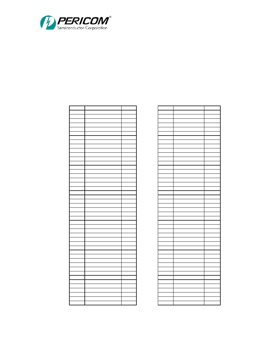
PI7C7300A
3-PORT PCI-TO-PCI BRIDGE
ADVANCE INFORMATION
Page 98 OF 109
09/25/03 Revision 1.09
master. The bus master can be either automatic test equipment or a component (i.e., PLD)
that interfaces to the TAP. The TAP controller changes state only in response to a rising
edge of TCK. The value of the test mode state (TMS) input signal at a rising edge of
TCK controls the sequence of state changes. The TAP controller is initialized after
power-up by applying a low to the TRST# pin. In addition, the TAP controller can be
initialized by applying a high signal level on the TMS input for a minimum of five TCK
periods.
For greater detail on the behavior of the TAP controller, test logic in each controller state
and the state machine and public instructions, refer to the IEEE 1149.1 Standard Test
Access Port and Boundary-Scan Architecture document (available from the IEEE).
Table 16-2 JTAG BOUNDARY REGISTER ORDER
Order
Pin Names
Type
Order
Pin Names
Type
0 ENUM#
output
60 P_STOP# control
1 ENUM#
control
61 P_PERR# bidir
2 HS_EN
input
62 P_PERR# control
3 S_CFN#
input
63 P_LOCK# input
4 S1_EN
input
64 P_SERR# output
5 S2_EN
input
65 P_SERR# control
6 SCAN_TM#
input
66 P_AD[13] bidir
7 SCAN_EN
input
67 P_AD[13] control
8 PLL_TM
input
68 P_AD[14] bidir
9 BYPASS
input
69 P_AD[14] control
10 S2_M66EN
input
70 P_AD[11]
bidir
11 P_RESET#
input
71 P_AD[11]
control
12 P_GNT#
input
72 P_AD[15]
bidir
13 P_REQ#
output
73 P_AD[15]
control
14 P_REQ#
control
74 P_AD[12]
bidir
15 P_AD[30]
bidir
75 P_AD[12]
control
16 P_AD[30]
control
76 P_AD[8]
bidir
17 P_AD[31]
bidir
77 P_AD[8]
control
18 P_AD[31]
control
78 P_CBE[1]
bidir
19 P_AD[27]
bidir
79 P_CBE[1]
control
20 P_AD[27]
control
80 P_AD[9]
bidir
21 P_AD[26]
bidir
81 P_AD[9]
control
22 P_AD[26]
control
82 P_AD[5]
bidir
23 P_AD[28]
bidir
83 P_AD[5]
control
24 P_AD[28]
control
84 P_M66EN
input
25 P_AD[29]
bidir
85 P_AD[6]
bidir
26 P_AD[29]
control
86 P_AD[6]
control
27 P_CBE[3]
bidir
87 P_AD[2]
bidir
28 P_CBE[3]
control
88 P_AD[2]
control
29 P_AD[24]
bidir
89 P_PAR
bidir
30 P_AD[24]
control
90 P_PAR
control
31 P_AD[25]
bidir
91 P_AD[0]
bidir
32 P_AD[25]
control
92 P_AD[0]
control
33 P_AD[23]
bidir
93 P_CBE[0]
bidir
34 P_AD[23]
control
94 P_CBE[0]
control
35 P_AD[22]
bidir
95 P_AD[7]
bidir
36 P_AD[22]
control
96 P_AD[7]
control
37 P_IDSEL
input
97 P_AD[10]
bidir
38 P_AD[21]
bidir
98 P_AD[10]
control
39 P_AD[21]
control
99 P_AD[1]
bidir
40 P_AD[20]
bidir
100 P_AD[1]
control
41 P_AD[20]
control
101 P_AD[3]
bidir
42 P_AD[19]
bidir
102 P_AD[3]
control
43 P_AD[19]
control
103 P_AD[4]
bidir
44 P_AD[18]
bidir
104 P_AD[4]
control
45 P_AD[18]
control
105 S1_AD[0]
bidir
PI7C7300A
3-PORT PCI-TO-PCI BRIDGE
ADVANCE INFORMATION
Page 99 OF 109
09/25/03 Revision 1.09
Order
Pin Names
Type
Order
Pin Names
Type
46 P_AD[17]
bidir
106 S1_AD[0]
control
47 P_AD[17]
control
107 S1_AD[1]
bidir
48 P_AD[16]
bidir
108 S1_AD[1]
control
49 P_AD[16]
control
109 S1_AD[2]
bidir
50 P_CBE[2]
bidir
110 S1_AD[2]
control
51 P_CBE[2]
control
111 S1_AD[5]
bidir
52 P_FRAME#
bidir
112 S1_AD[5]
control
53 P_FRAME#
control
113 S1_AD[3]
bidir
54 P_IRDY#
bidir
114 S1_AD[3]
control
55 P_IRDY#
control
115 S1_AD[4]
bidir
56 P_TRDY#
bidir
116 S1_AD[4]
control
57
P_DEVSEL#/P_TRDY#
control
117
S1_CBE[0]
bidir
58 P_DEVSEL#
bidir
118 S1_CBE[0] control
59 P_STOP#
bidir
119 S1_AD[7]
bidir
120 S1_AD[7]
control
182 S1_AD[28]
control
121 S1_AD[6]
bidir
183 S1_AD[30]
bidir
122 S1_AD[6]
control
184 S1_AD[30]
control
123 S1_AD[8]
bidir
185 S1_AD[31]
bidir
124 S1_AD[8]
control
186 S1_AD[31]
control
125 S1_AD[9]
bidir
187 S1_AD[27]
bidir
126 S1_AD[9]
control
188 S1_AD[27]
control
127 S1_AD[10]
bidir
189 S1_AD[24]
bidir
128 S1_AD[10]
control
190 S1_AD[24]
control
129 S1_AD[11]
bidir
191 S1_AD[18]
bidir
130 S1_AD[11]
control
192 S1_AD[18]
control
131 S1_AD[12]
bidir
193 S1_GNT#[0] output
132 S1_AD[12]
control
194 S1_GNT#[0] control
133 S1_AD[14]
bidir
195 S1_REQ#[0] input
134 S1_AD[14]
control
196 S1_REQ#[1] input
135 S1_AD[13]
bidir
197 S1_GNT#[1] output
136 S1_AD[13]
control
198 S1_GNT#[2] output
137 S1_AD[15]
bidir
199 S1_REQ#[2] input
138 S1_AD[15]
control
200 S1_REQ#[3] input
139 S1_SERR#
input
201 S1_GNT#[3] output
140 S1_PAR
bidir
202 S1_GNT#[4] output
141 S1_PAR
control
203 S1_REQ#[4] input
142 S1_CBE[1]
bidir
204 S1_REQ#[5] input
143 S1_CBE[1]
control
205 S1_GNT#[5] output
144 S1_DEVSEL#
bidir
206 S1_GNT#[6] output
145
S1_DEVSEL#/S1_TRDY#
control
207
S1_REQ#[6]
input
146 S1_STOP#
bidir
208 S1_REQ#[7] input
147 S1_STOP#
control
209 S1_GNT#[7] output
148 S1_LOCK#
bidir
210 S1_RESET# output
149 S1_LOCK#
control
211 S2_AD[0]
bidir
150 S1_PERR#
bidir
212 S2_AD[0]
control
151 S1_PERR#
control
213 S2_AD[1]
bidir
152 S1_FRAME#
bidir
214 S2_AD[1]
control
153 S1_FRAME#
control
215 S2_AD[2]
bidir
154 S1_IRDY#
bidir
216 S2_AD[2]
control
155 S1_IRDY#
control
217 S2_AD[3]
bidir
156 S1_TRDY#
bidir
218 S2_AD[3]
control
157 S1_AD[17]
bidir
219 S2_AD[4]
bidir
158 S1_AD[17]
control
220 S2_AD[4]
control
159 S1_AD[16]
bidir
221 S2_AD[5]
bidir
160 S1_AD[16]
control
222 S2_AD[5]
control
161 S1_AD[20]
bidir
223 S2_AD[6]
bidir
162 S1_AD[20]
control
224 S2_AD[6]
control
163 S1_CBE[2]
bidir
225 S2_AD[7]
bidir
164 S1_CBE[2]
control
226 S2_AD[7]
control
165 S1_AD[19]
bidir
227 S2_CBE[0]
bidir
166 S1_AD[19]
control
228 S2_CBE[0]
control
167 S1_CBE[3]
bidir
229 S2_AD[8]
bidir
168 S1_CBE[3]
control
230 S2_AD[8]
control
PI7C7300A
3-PORT PCI-TO-PCI BRIDGE
ADVANCE INFORMATION
Page 100 OF 109
09/25/03 Revision 1.09
Order
Pin Names
Type
Order
Pin Names
Type
169 S1_AD[23]
bidir
231 S2_AD[10]
bidir
170 S1_AD[23]
control
232 S2_AD[10]
control
171 S1_AD[26]
bidir
233 S2_AD[9]
bidir
172 S1_AD[26]
control
234 S2_AD[9]
control
173 S1_AD[22]
bidir
235 S2_AD[11]
bidir
174 S1_AD[22]
control
236 S2_AD[11]
control
175 S1_AD[25]
bidir
237 S1_M66EN
Input
176 S1_AD[25]
control
238 S2_AD[12]
bidir
177 S1_AD[29]
bidir
239 S2_AD[12]
control
178 S1_AD[29]
control
240 S2_AD[14]
bidir
179 S1_AD[21]
bidir
241 S2_AD[14]
control
180 S1_AD[21]
control
242 S2_CBE[1]
bidir
181 S1_AD[28]
bidir
243 S2_CBE[1]
control
244 S2_AD[15]
bidir
282 S2_AD[23]
bidir
245 S2_AD[15]
control
283 S2_AD[23]
control
246 S2_PAR
bidir
284 S2_CBE[3]
bidir
247 S2_PAR
control
285 S2_CBE[3]
control
248 S2_SERR#
input
286 S2_AD[25]
bidir
249 S2_LOCK#
bidir
287 S2_AD[25]
control
250 S2_LOCK#
control
288 S2_AD[26]
bidir
251 S2_TRDY#
bidir
289 S2_AD[26]
control
252
S2_DEVSEL#/S2_TRDY#
control
290
S2_AD[28]
bidir
253 S2_STOP#
bidir
291 S2_AD[28]
control
254 S2_STOP#
control
292 S2_AD[27]
bidir
255 S2_IRDY#
bidir
293 S2_AD[27]
control
256 S2_IRDY#
control
294 S2_AD[29]
bidir
257 S2_CBE[2]
bidir
295 S2_AD[29]
control
258 S2_CBE[2]
control
296 S2_AD[30]
bidir
259 S2_AD[13]
bidir
297 S2_AD[30]
control
260 S2_AD[13]
control
298 S2_AD[31]
bidir
261 S2_AD[21]
bidir
299 S2_AD[31]
control
262 S2_AD[21]
control
300 S2_GNT#[0] output
263 S2_PERR#
bidir
301 S2_GNT#[0] control
264 S2_PERR#
control
302 S2_REQ#[0] input
265 S2_AD[16]
bidir
303 S2_REQ#[1] input
266 S2_AD[16]
control
304 S2_GNT#[1] output
267 S2_FRAME#
bidir
305 S2_GNT#[2] output
268 S2_FRAME#
control
306 S2_REQ#[2] input
269 S2_DEVSEL#
bidir
307 S2_REQ#[3] input
270 S2_AD[19]
bidir
308 S2_GNT#[3] output
271 S2_AD[19]
control
309 S2_GNT#[4] output
Order
Pin Names
Type
Order
Pin Names
Type
272 S2_AD[17]
bidir
310 S2_REQ#[4] input
273 S2_AD[17]
control
311 S2_REQ#[5] input
274 S2_AD[18]
bidir
312 S2_GNT#[5] output
275 S2_AD[18]
control
313 S2_GNT#[6] output
276 S2_AD[20]
bidir
314 S2_REQ#[6] input
277 S2_AD[20]
control
278 S2_AD[22]
bidir
279 S2_AD[22]
control
280 S2_AD[24]
bidir
281 S2_AD[24]
control
17
ELECTRICAL AND TIMING SPECIFICATIONS
PI7C7300A
3-PORT PCI-TO-PCI BRIDGE
ADVANCE INFORMATION
Page 101 OF 109
09/25/03 Revision 1.09
17.1
MAXIMUM RATINGS
(Above which the useful life may be impaired. For user guidelines, not tested).
Storage Temperature
-65
°C to 150°C
Ambient Temperature with Power Applied
-40
°C to 85°C
Supply Voltage to Ground Potentials (Inputs and AV
CC
, V
DD
only]
-0.3V to 3.6V
DC Input Voltage
-0.5V to 3.6V
Note:
Stresses greater than those listed under MAXIMUM RATINGS may cause permanent
damage to the device. This is a stress rating only and functional operation of the device at
these or any conditions above those indicated in the operational sections of this
specification is not implied. Exposure to absolute maximum rating conditions for
extended periods of time may affect reliability.
17.2
3.3V DC SPECIFICATIONS
Symbol Parameter
Condition
Min.
Max.
Units Notes
V
DD
,
AV
CC
Supply Voltage
3
3.6
V
V
ih
Input HIGH Voltage
0.5 V
DD
V
DD
+ 0.5
V
3
V
il
Input LOW Voltage
-0.5
0.3 V
DD
V 3
V
ih
CMOS Input HIGH Voltage
0.7 V
DD
V
DD
+ 0.5
V
1
V
il
CMOS Input LOW Voltage
-0.5
0.3 V
DD
V 1
V
ipu
Input Pull-up Voltage
0.7 V
DD
V 3
I
il
Input Leakage Current
0 < V
in
< V
DD
±10
µA
3
V
oh
Output HIGH Voltage
I
out
= -500
µA
0.9V
DD
V
3
V
ol
Output LOW Voltage
I
out
= 1500
µA
0.1
V
DD
V
3
V
oh
CMOS Output HIGH Voltage
I
out
= -500
µA
V
DD
0.5
V
2
V
ol
CMOS Output LOW Voltage
I
out
= 1500
µA
0.5
V
2
C
in
Input Pin Capacitance
10
pF
3
C
CLK
CLK Pin Capacitance
5
12
pF
3
C
IDSEL
IDSEL Pin Capacitance
8
pF
3
L
pin
Pin
Inductance
20 nH
3
Notes:
1. CMOS Input pins: S_CFN#, TCK, TMS, TDI, TRST#, SCAN_EN, SCAN_TM#
2. CMOS Output pin: TDO
3.
PCI pins: P_AD[31:0], P_CBE[3:0], P_PAR, P_FRAME#, P_IRDY#, P_TRDY#,
P_DEVSEL#, P_STOP#, P_LOCK#, PIDSEL#, P_PERR#, P_SERR#, P_REQ#, P_GNT#,
P_RESET#, S1_AD[31:0], S2_AD[31:0], S1_CBE[3:0], S2_CBE[3:0], S1_PAR, S2_PAR,
S1_FRAME#, S2_FRAME#, S1_IRDY#, S2_IRDY#, S1_TRDY#, S2_TRDY#,
S1_DEVSEL#, S2_DEVSEL#, S1_STOP#, S2_STOP#, S1_LOCK#, S2_LOCK#,
S1_PERR#, S2_PERR#, S1_SERR#, S2_SERR#, S1_REQ[7:0]#, S2_REQ[6:0]#,
S1_GNT[7:0]#, S2_GNT[6:0], S1_RESET#, S2_RESET#, S1_EN, S2_EN, HSLED,
HS_SW#, HS_EN, ENUM#.
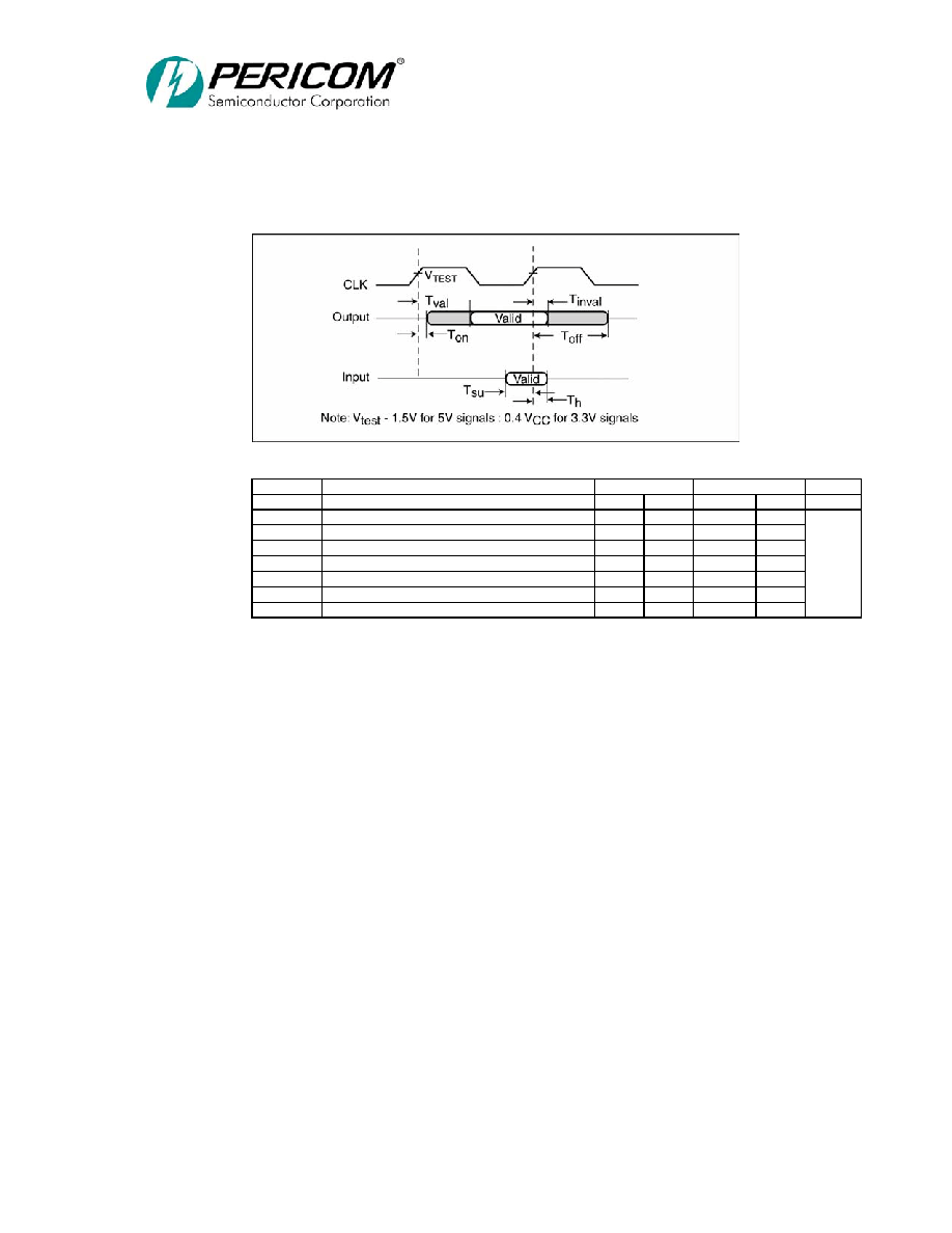
PI7C7300A
3-PORT PCI-TO-PCI BRIDGE
ADVANCE INFORMATION
Page 102 OF 109
09/25/03 Revision 1.09
17.3
3.3V AC SPECIFICATIONS
Figure 17-1 PCI SIGNAL TIMING MEASUREMENT CONDITIONS
66 MHz
33 MHz
Symbol Parameter
Min. Max. Min.
Max. Units
Tsu
Input setup time to CLK bused signals
1,2,3
3
-
7 -
Tsu(ptp)
Input setup time to CLK point-to-point
1,2,3
5
- 10,
12
4
-
Th
Input signal hold time from CLK
1,2
0
-
0
-
Tval
CLK to signal valid delay bused signals
1,2,3
2 6 2
11
Tval(ptp)
CLK to signal valid delay point-to-point
1,2,3
2 6 2
12
Ton
Float to active delay
1,2
2
-
2
-
Toff
Active to float delay
1,2
-
14
-
28
ns
1. See Figure 17-1 PCI Signal Timing Measurement Conditions.
2. All primary interface signals are synchronized to P_CLK. All secondary interface
signals are synchronized to either S1_CLKOUT or S2_CLKOUT.
3. Point-to-point signals are P_REQ#, S1_REQ#[7:0], S2_REQ#[6:0], P_GNT#,
S1_GNT#[7:0], S2_GNT#[6:0], HSLED, HS_SW#, HS_EN, and ENUM#. Bused
signals are P_AD, P_BDE#, P_PAR, P_PERR#, P_SERR#, P_FRAME#, P_IRDY#,
P_TRDY#, P_LOCK#, P_DEVSEL#, P_STOP#, P_IDSEL, S1_AD, S1_CBE#,
S1_PAR, S1_PERR#, S1_SERR#, S1_FRAME#, S1_IRDY#, S1_TRDY#,
S1_LOCK#, S1_devsel#, S1_STOP#, S2_AD, S2_CBE#, S2_PAR, S2_PERR#,
S2_SERR#, S2_FRAME#, S2_IRDY#, S2_TRDY#, S2_LOCK#, S2_DEVSEL#,
and S2_STOP#.
4. REQ# signals have a setup of 10 and GNT# signals have a setup of 12.
PI7C7300A
3-PORT PCI-TO-PCI BRIDGE
ADVANCE INFORMATION
Page 103 OF 109
09/25/03 Revision 1.09
17.4
PRIMARY AND SECONDARY BUSES AT 66MHz
CLOCK TIMING
Symbol Parameter
Condition
Min. Max. Units
T
SKEW
SKEW among S1_CLKOUT[7:0]
0
250
T
SKEW
SKEW among S2_CLKOUT[6:0]
0
250
ps
T
DELAY
DELAY between PCLK and S1_CLKOUT[7:0] 20pF
load
3.3
4.9
T
DELAY
DELAY between PCLK and S2_CLKOUT[6:0] 20pF
load
3.3
4.9
T
CYCLE
PCLK, S1_CLKOUT[7:0] cycle time
15
30
T
CYCLE
PCLK, S2_CLKOUT[6:0] cycle time
15
30
T
HIGH
PCLK, S1_CLKOUT[7:0] HIGH time
6
T
HIGH
PCLK, S2_CLKOUT[6:0] HIGH time
6
T
LOW
PCLK, S1_CLKOUT[7:0] LOW time
6
T
LOW
PCLK, S_CLKOUT[6:0] LOW time
6
ns
17.5
PRIMARY AND SECONDARY BUSES AT 33MHz
CLOCK TIMING
Symbol Parameter
Condition
Min. Max. Units
T
SKEW
SKEW among S1_CLKOUT[7:0]
0
250
T
SKEW
SKEW among S2_CLKOUT[6:0]
0
250
ps
T
DELAY
DELAY between PCLK and S1_CLKOUT[7:0] 20pF
load
3.3
4.9
T
DELAY
DELAY between PCLK and S2_CLKOUT[6:0] 20pF
load
3.3
4.9
T
CYCLE
PCLK, S1_CLKOUT[7:0] cycle time
30
T
CYCLE
PCLK, S2_CLKOUT[6:0] cycle time
30
T
HIGH
PCLK, S1_CLKOUT[7:0] HIGH time
11
T
HIGH
PCLK, S2_CLKOUT[6:0] HIGH time
11
T
LOW
PCLK, S1_CLKOUT[7:0] LOW time
11
T
LOW
PCLK, S2_CLKOUT[6:0] LOW time
11
ns
17.6
POWER CONSUMPTION
Parameter Typical
Units
Power Consumption
2178
mW
Supply Current, I
CC
660
mA
Note: Typical values are at VCC = 3.3V, TA = 25°C, and all three ports running at 66MHz.
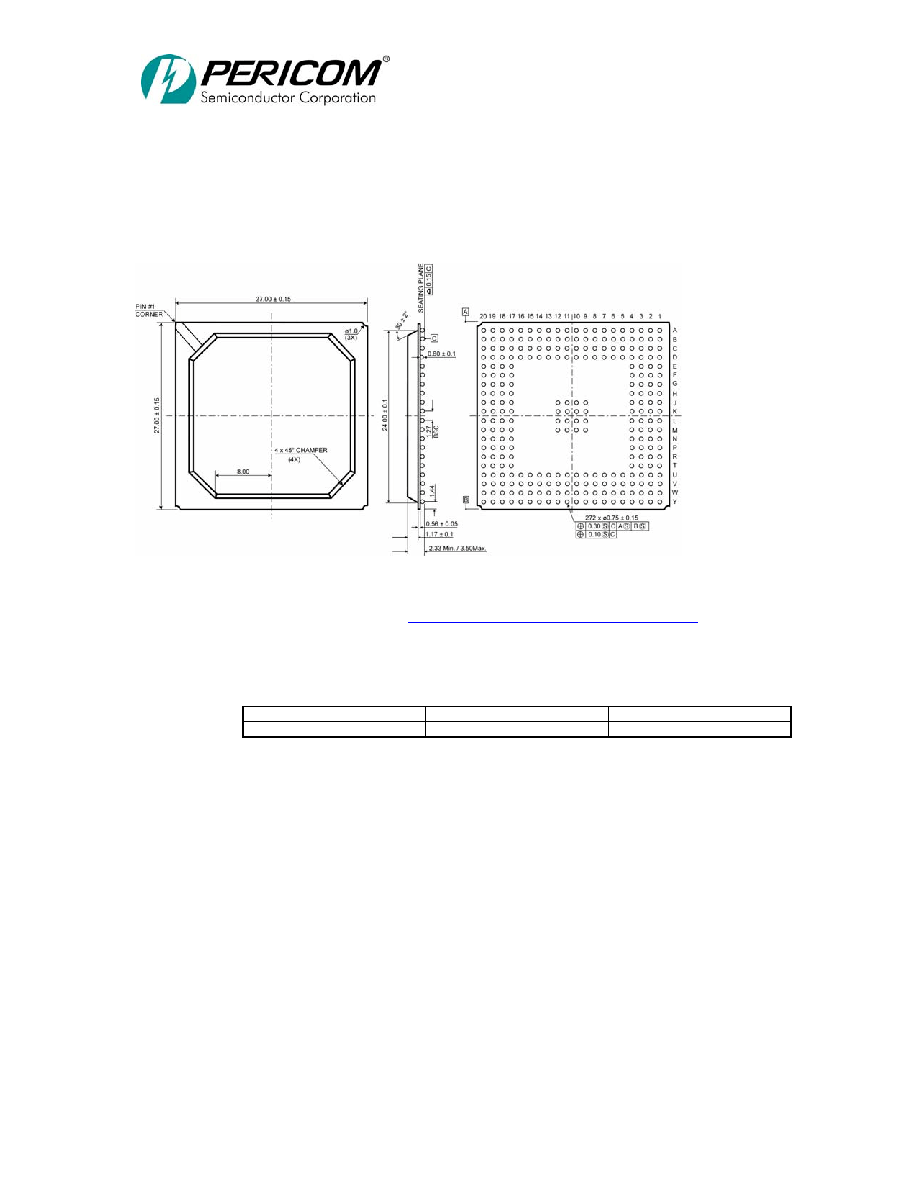
PI7C7300A
3-PORT PCI-TO-PCI BRIDGE
ADVANCE INFORMATION
Page 104 OF 109
09/25/03 Revision 1.09
18
272-PIN PBGA PACKAGE FIGURE
Figure 18-1 272-PIN PBGA PACKAGE
TOP
BOTTOM
Thermal Characteristics can be found on the web:
http://www.pericom.com/packaging/mechanicals.php
18.1
PART NUMBER ORDERING INFORMATION
Part Number
Pin Package
Temperature
PI7C7300ANA
272 PBGA
-40
°C to 85°C
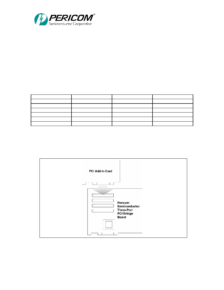
PI7C7300A
3-PORT PCI-TO-PCI BRIDGE
ADVANCE INFORMATION
Page 105 OF 109
09/25/03 Revision 1.09
APPENDIX A: PI7C7300A EVALUATION BOARD USER'S
MANUAL
GENERAL INFORMATION
1. Please make sure you have included with your PI7C7300A evaluation board, the five-page schematic
and the preliminary specification for the PI7C7300A.
2. Check all jumpers for proper settings:
Pin Name
Jumper
Function
Position
S_CFN#
JP4
Internal Arbiter Enable
1-2 (0)
S1_EN
JP5
S1 Bus Enable
2-3 (1)
S2_EN
JP6
S2 Bus Enable
2-3 (1)
SCAN_EN
JP7
Scan Control
1-2 (0)
PLL_TM
JP8
PLL test mode disable
1-2 (0)
BYPASS
JP9
PLL disable
2-3 (1)
3. Check and make sure there are no shorts between power (3.3V, 5V, 12V, and 12V) and ground.
4. Plug evaluation board in any PCI slot on your system. Make sure your system is powered off before
doing so.
5. Connect any PCI devices on the secondary slots of the evaluation board. Be careful that the
orientation of the card is correct (see Diagram A).
Diagram A

PI7C7300A
3-PORT PCI-TO-PCI BRIDGE
ADVANCE INFORMATION
Page 106 OF 109
09/25/03 Revision 1.09
GENERAL INFORMATION (continued)
6. Turn on the power for the system. Your OS should already have drivers for the PI7C7300A evaluation
board. In Win9X, Plug and Play should detect the device as a PCI-to-PCI bridge. The system may
prompt you for the Win9X CD for the drivers. The OS will detect two PCI-to-PCI bridges as the
PI7C7300A has two secondary PCI buses. In Win NT, you should not have to install drivers.
7. Install drivers for any PCI devices you have attached to the evaluation board.
8. If any of the steps are unclear or were unsuccessful, please contact your Pericom support person at
408-435-0800.
9. Thank for evaluating Pericom Semiconductor Corporation's products.

PI7C7300A
3-PORT PCI-TO-PCI BRIDGE
ADVANCE INFORMATION
Page 107 OF 109
09/25/03 Revision 1.09
FREQUENTLY ASKED QUESTIONS
!
What is the function of SCAN_EN?
SCAN_EN is for a full scan test or S_CLKIN select. During SCAN mode, SCAN_EN will be driven
to logic "0" or "logic "1" depending on functionality. During normal mode, if SCAN_EN is
connected to logic "0" (JP7 in the 1-2 position), S_CLKIN will be used for PLL test only when
PL_TM is active.
!
What is the function of SCAN_TM#?
SCAN_TM# is for full scan test and power on reset for the PLL. SCAN_TM# should be connected to
logic "1" or to an RC path (R1 and C13) during normal operation.
!
How do you use the external arbiter?
a) Disable the on chip arbiter by connecting S_CFN to logic "1" (JP4 in the 2-3 position).
b) Use S1_REQ#[0] as GRANT and S1_GNT#[0] as REQUEST on the S1 bus.
c) Use S2_REQ#[0] as GRANT and S2_GNT#[0] as REQUEST on the S2 bus.
!
What is the purpose of having JP1, JP2, and JP3?
JP1, JP2, and JP3 are designed for easy access to the primary bus signals. You may connect any of
these pins to an oscilloscope or a logic analyzer for observation. No connection is required for normal
operation. The following table indicates which bus signals correspond to which pins.
1 2 3 4 5 6 7 8 9 10 11 12 13
14
15
16
JP2 REQ AD29 AD26 CBE3 AD21 AD21 CBE2 IRDY LOCK PAR AD14 AD11 CBE0 AD6 AD5 AD0
JP3 AD31 AD28 AD25 AD23 AD20 AD20 FRAME DVSEL PERR CBE1 AD13 AD10 AD8 AD4 AD2 GND
JP1 GNT AD30 AD27 AD24 AD22 AD22 AD24 IRDY STOP SERR AD15 AD12 AD9 AD7 AD3 AD1
!
What is the purpose for having U17, U19, and U20?
U17, U19, and U20 are designed for easy access to the digital ground planes for observation.
!
How is the evaluation board constructed?
The evaluation board is a six-layer PCB. The top and bottom layers (1 and 6) are for signals, power,
and ground routing. Layer 2 and layer 5 are ground planes. Layer 3 is a digital 3.3V power plane.
Layer 4 is a digital 5V power plane with an island of analog 3.3V power.
!
What is the function of S_CLKIN?
The S_CLKIN pin is a test pin for the on chip PLL when PLL_TM is set to logic "1".

PI7C7300A
3-PORT PCI-TO-PCI BRIDGE
ADVANCE INFORMATION
Page 108 OF 109
09/25/03 Revision 1.09
!
What clock frequency combinations does the PI7C7300A support?
Primary
Secondary 1
Secondary 2
66MHz 66MHz 66MHz
66MHz 66MHz 33MHz
66MHz 33MHz 66MHz
66MHz 33MHz 33MHz
33MHz 33MHz 33MHz
50MHz 50MHz 50MHz
50MHz 50MHz 25MHz
50MHz 25MHz 50MHz
50MHz 25MHz 25MHz
25MHz 25MHz 25MHz
!
How are the JTAG signals being connected?
The JTAG signals consist of TRST#, TCK, TMS, TDI, and TDO. All the mentioned signals have
weak internal pull-up connections. Therefore, no connection is needed if you want the JTAG circuit to
be disabled. If you want to activate the JTAG circuit, you need to connect all five signals according to
the JTAG specification (IEEE 1149).

PI7C7300A
3-PORT PCI-TO-PCI BRIDGE
ADVANCE INFORMATION
Page 109 OF 109
09/25/03 Revision 1.09
NOTES: