 | ÐлекÑÑоннÑй компоненÑ: PI7C8148A | СкаÑаÑÑ:  PDF PDF  ZIP ZIP |
Äîêóìåíòàöèÿ è îïèñàíèÿ www.docs.chipfind.ru

PI7C8148A
2-Port PCI-to-PCI Bridge
REVISION 1.04
3545 North First Street, San Jose, CA 95134
Telephone: 1-877-PERICOM, (1-877-737-4266)
Fax: 408-435-1100
Email:
solutions@pericom.com
Internet:
http://www.pericom.com

PI7C8148A
2-PORT PCI-TO-PCI BRIDGE
ADVANCE INFORMATION
Page 2 of 90
JUNE 2004 Revision 1.04
LIFE SUPPORT POLICY
Pericom Semiconductor Corporation's products are not authorized for use as critical components in life support
devices or systems unless a specific written agreement pertaining to such intended use is executed between the
manufacturer and an officer of PSC.
1) Life support devices or system are devices or systems which:
a) Are intended for surgical implant into the body or
b) Support or sustain life and whose failure to perform, when properly used in accordance with
instructions for use provided in the labeling, can be reasonably expected to result in a significant injury
to the user.
2) A critical component is any component of a life support device or system whose failure to perform can be
reasonably expected to cause the failure of the life support device or system, or to affect its safety or
effectiveness. Pericom Semiconductor Corporation reserves the right to make changes to its products or
specifications at any time, without notice, in order to improve design or performance and to supply the best
possible product. Pericom Semiconductor does not assume any responsibility for use of any circuitry
described other than the circuitry embodied in a Pericom Semiconductor product. The Company makes no
representations that circuitry described herein is free from patent infringement or other rights of third parties
which may result from its use. No license is granted by implication or otherwise under any patent, patent
rights or other rights, of Pericom Semiconductor Corporation.
All other trademarks are of their respective companies.

PI7C8148A
2-PORT PCI-TO-PCI BRIDGE
ADVANCE INFORMATION
Page 3 of 90
JUNE 2004 Revision 1.04
REVISION HISTORY
DATE REVISION
NUMBER
DESCRIPTION
11-13-2003
0.01
First Draft of Datasheet
03-25-2004
0.02
First release of preliminary datasheet
04-26-2004
0.03
Revisions/changes to GPIO and EEPROM references
05-10-2004
1.00
Revisions to EEPROM references
Revisions to ordering information, correction to package
codes
05-17-2004
1.01
Further modifications to EEPROM information
05-19-2004
1.02
Changed type for "Data Select" in 15.2.41 from RO to RW
06-11-2004
1.03
Added power consumptions data in section 16.6
Added T
DELAY
data in sections 16.4 and 16.5
06-14-2004
1.04
Revised descriptions in sections 15.2.39, 15.2.47, and 15.2.48.
Added VPD register descriptions (section 15.2.50 15.2.53)

PI7C8148A
2-PORT PCI-TO-PCI BRIDGE
ADVANCE INFORMATION
Page 4 of 90
JUNE 2004 Revision 1.04
This page intentionally left blank.

PI7C8148A
2-PORT PCI-TO-PCI BRIDGE
ADVANCE INFORMATION
Page 5 of 90
JUNE 2004 Revision 1.04
TABLE OF CONTENTS
1
SIGNAL DEFINITIONS.............................................................................................................................13
1.1
SIGNAL
TYPES....................................................................................................................................13
1.2
SIGNALS ..............................................................................................................................................13
1.2.1
PRIMARY BUS INTERFACE SIGNALS ...................................................................................13
1.2.2
SECONDARY BUS INTERFACE SIGNALS .............................................................................14
1.2.3
CLOCK SIGNALS ........................................................................................................................16
1.2.4
MISCELLANEOUS SIGNALS ....................................................................................................16
1.2.5
GENERAL PURPOSE I/O INTERFACE SIGNALS .................................................................17
1.2.6
POWER AND GROUND..............................................................................................................17
1.3
PIN
LIST
160-PIN
LFBGA.................................................................................................................18
2
PCI BUS OPERATION...............................................................................................................................19
2.1
TYPES
OF
TRANSACTIONS ..............................................................................................................19
2.2
SINGLE
ADDRESS
PHASE.................................................................................................................20
2.3
DEVICE
SELECT
(DEVSEL#)
GENERATION ..................................................................................20
2.4
DATA
PHASE.......................................................................................................................................20
2.5
WRITE
TRANSACTIONS....................................................................................................................20
2.5.1
MEMORY WRITE TRANSACTIONS.........................................................................................21
2.5.2
MEMORY WRITE AND INVALIDATE .....................................................................................22
2.5.3
DELAYED WRITE TRANSACTIONS ........................................................................................22
2.5.4
WRITE TRANSACTION BOUNDARIES...................................................................................23
2.5.5
BUFFERING MULTIPLE WRITE TRANSACTIONS..............................................................23
2.5.6
FAST BACK-TO-BACK TRANSACTIONS ................................................................................23
2.6
READ
TRANSACTIONS .....................................................................................................................24
2.6.1
PREFETCHABLE READ TRANSACTIONS.............................................................................24
2.6.2
DYNAMIC PREFETCHING CONTROL....................................................................................24
2.6.3
NON-PREFETCHABLE READ TRANSACTIONS ...................................................................24
2.6.4
READ PREFETCH ADDRESS BOUNDARIES ........................................................................25
2.6.5
DELAYED READ REQUESTS ...................................................................................................25
2.6.6
DELAYED READ COMPLETION WITH TARGET .................................................................26
2.6.7
DELAYED READ COMPLETION ON INITIATOR BUS.........................................................26
2.6.8
FAST BACK-TO-BACK READ TRANSACTIONS ....................................................................27
2.7
CONFIGURATION
TRANSACTIONS................................................................................................27
2.7.1
TYPE 0 ACCESS TO PI7C8148A................................................................................................28
2.7.2
TYPE 1 TO TYPE 0 CONVERSION ...........................................................................................28
2.7.3
TYPE 1 TO TYPE 1 FORWARDING ..........................................................................................29
2.7.4
SPECIAL CYCLES.......................................................................................................................30
2.8
TRANSACTION
TERMINATION.......................................................................................................30
2.8.1
MASTER TERMINATION INITIATED BY PI7C8148A ..........................................................31
2.8.2
MASTER ABORT RECEIVED BY PI7C8148A .........................................................................32
2.8.3
TARGET TERMINATION RECEIVED BY PI7C8148A ...........................................................32
2.8.4
TARGET TERMINATION INITIATED BY PI7C8148A...........................................................34
3
ADDRESS DECODING..............................................................................................................................36
3.1
ADDRESS
RANGES ............................................................................................................................36
3.2
I/O
ADDRESS
DECODING..................................................................................................................36
3.2.1
I/O BASE AND LIMIT ADDRESS REGISTER .........................................................................37
3.2.2
ISA MODE ....................................................................................................................................37
3.3
MEMORY
ADDRESS
DECODING.....................................................................................................38
3.3.1
MEMORY-MAPPED I/O BASE AND LIMIT ADDRESS REGISTERS ..................................38
3.3.2
PREFETCHABLE MEMORY BASE AND LIMIT ADDRESS REGISTERS ..........................39

PI7C8148A
2-PORT PCI-TO-PCI BRIDGE
ADVANCE INFORMATION
Page 6 of 90
JUNE 2004 Revision 1.04
3.4
VGA
SUPPORT ....................................................................................................................................40
3.4.1
VGA MODE ..................................................................................................................................40
3.4.2
VGA SNOOP MODE ....................................................................................................................40
4
TRANSACTION ORDERING ...................................................................................................................41
4.1
TRANSACTIONS
GOVERNED
BY
ORDERING
RULES .................................................................41
4.2
GENERAL
ORDERING
GUIDELINES ...............................................................................................42
4.3
ORDERING
RULES .............................................................................................................................43
4.4
DATA
SYNCHRONIZATION .............................................................................................................44
5
ERROR HANDLING ..................................................................................................................................44
5.1
ADDRESS
PARITY
ERRORS..............................................................................................................44
5.2
DATA
PARITY
ERRORS.....................................................................................................................45
5.2.1
CONFIGURATION WRITE TRANSACTIONS TO CONFIGURATION SPACE ...................45
5.2.2
READ TRANSACTIONS .............................................................................................................45
5.2.3
DELAYED WRITE TRANSACTIONS ........................................................................................46
5.2.4
POSTED WRITE TRANSACTIONS ...........................................................................................48
5.3
DATA
PARITY
ERROR
REPORTING
SUMMARY...........................................................................49
5.4
SYSTEM
ERROR
(SERR#)
REPORTING ...........................................................................................52
6
PCI BUS ARBITRATION ..........................................................................................................................53
6.1
PRIMARY
PCI
BUS
ARBITRATION..................................................................................................53
6.2
SECONDARY
PCI
BUS
ARBITRATION............................................................................................53
6.2.1
PREEMPTION .............................................................................................................................53
6.2.2
BUS PARKING.............................................................................................................................54
7
CLOCKS ......................................................................................................................................................54
7.1
PRIMARY
CLOCK
INPUTS ................................................................................................................54
7.2
SECONDARY
CLOCK
OUTPUTS ......................................................................................................54
7.3
PCI
CLOCKRUN ..................................................................................................................................54
8
GENERAL PURPOSE I/O INTERFACE.................................................................................................55
8.1
GPIO
CONTROL
REGISTERS ............................................................................................................55
9
EEPROM INTERFACE .............................................................................................................................55
9.1
AUTO
MODE
EEPROM
ACCESS .......................................................................................................55
9.2
EEPROM
MODE
AT
RESET................................................................................................................56
9.3
EEPROM
DATA
STRUCTURE ...........................................................................................................56
9.4
EEPROM
SPACE
ADDRESS
MAP......................................................................................................56
9.4.1
EEPROM CONTENT...................................................................................................................56
10
COMPACT PCI HOT SWAP.................................................................................................................58
11
PCI POWER MANAGEMENT .............................................................................................................58
12
RESET ......................................................................................................................................................59
12.1
PRIMARY
INTERFACE
RESET..........................................................................................................59
12.2
SECONDARY
INTERFACE
RESET ...................................................................................................59
12.3
CHIP
RESET .........................................................................................................................................60
13
SUPPORTED COMMANDS..................................................................................................................60
13.1
PRIMARY
INTERFACE ......................................................................................................................60
13.2
SECONDARY
INTERFACE ................................................................................................................61

PI7C8148A
2-PORT PCI-TO-PCI BRIDGE
ADVANCE INFORMATION
Page 7 of 90
JUNE 2004 Revision 1.04
14
BRIDGE BEHAVIOR.............................................................................................................................62
14.1
BRIDGE
ACTIONS
FOR
VARIOUS
CYCLE
TYPES.........................................................................62
14.2
ABNORMAL
TERMINATION
(INITIATED
BY
BRIDGE
MASTER) ..............................................63
14.2.1
MASTER ABORT.........................................................................................................................63
14.2.2
PARITY AND ERROR REPORTING .........................................................................................63
14.2.3
REPORTING PARITY ERRORS.................................................................................................63
14.2.4
SECONDARY IDSEL MAPPING................................................................................................63
15
CONFIGURATION REGISTERS.........................................................................................................64
15.1
REGISTER
TYPES ...............................................................................................................................64
15.2
CONFIGURATION
REGISTER...........................................................................................................64
15.2.1
VENDOR ID REGISTER OFFSET 00h ..................................................................................65
15.2.2
DEVICE ID REGISTER OFFSET 00h....................................................................................65
15.2.3
COMMAND REGISTER OFFSET 04h ...................................................................................65
15.2.4
PRIMARY STATUS REGISTER OFFSET 04h ......................................................................66
15.2.5
REVISION ID REGISTER OFFSET 08h................................................................................67
15.2.6
CLASS CODE REGISTER OFFSET 08h................................................................................67
15.2.7
CACHE LINE REGISTER OFFSET 0Ch ...............................................................................67
15.2.8
PRIMARY LATENCY TIMER REGISTER OFFSET 0Ch.....................................................67
15.2.9
HEADER TYPE REGISTER OFFSET 0Ch ............................................................................67
15.2.10
PRIMARY BUS NUMBER REGISTER OFFSET 18h .......................................................67
15.2.11
SECONDARY BUS NUMBER REGISTER OFFSET 18h .................................................68
15.2.12
SUBORDINATE BUS NUMBER REGISTER OFFSET 18h .............................................68
15.2.13
SECONDARY LATENCY TIMER REGISTER OFFSET 18h ...........................................68
15.2.14
I/O BASE ADDRESS REGISTER OFFSET 1Ch................................................................68
15.2.15
I/O LIMIT ADDRESS REGISTER OFFSET 1Ch ..............................................................68
15.2.16
SECONDARY STATUS REGISTER OFFSET 1Ch............................................................69
15.2.17
MEMORY BASE ADDRESS REGISTER OFFSET 20h ....................................................69
15.2.18
MEMORY LIMIT ADDRESS REGISTER OFFSET 20h ...................................................70
15.2.19
PREFETCHABLE MEMORY BASE ADDRESS REGISTER OFFSET 24h....................70
15.2.20
PREFETCHABLE MEMORY LIMIT ADDRESS REGISTER OFFSET 24h ..................70
15.2.21
PREFETCHABLE MEMORY BASE ADDRESS UPPER 32-BITS REGISTER OFFSET
28h ...................................................................................................................................................70
15.2.22
PREFETCHABLE MEMORY LIMIT ADDRESS UPPER 32-BITS REGISTER OFFSET
2Ch ...................................................................................................................................................71
15.2.23
I/O BASE ADDRESS UPPER 16-BITS REGISTER OFFSET 30h ...................................71
15.2.24
I/O LIMIT ADDRESS UPPER 16-BITS REGISTER OFFSET 30h ..................................71
15.2.25
CAPABILITY POINTER REGISTER OFFSET 34h ..........................................................71
15.2.26
INTERRUPT LINE REGISTER OFFSET 3Ch ..................................................................71
15.2.27
INTERRUPT PIN REGISTER OFFSET 3Ch .....................................................................71
15.2.28
BRIDGE CONTROL REGISTER OFFSET 3Ch ................................................................72
15.2.29
DIAGNOSTIC/CHIP CONTROL REGISTER OFFSET 40h .............................................73
15.2.30
ARBITER CONTROL REGISTER OFFSET 40h ...............................................................74
15.2.31
EXTENDED CHIP CONTROL REGISTER OFFSET 48h ................................................74
15.2.32
SECONDARY BUS ARBITER PREEMPTION CONTROL REGISTER OFFSET 4Ch ..75
15.2.33
P_SERR# EVENT DISABLE REGISTER OFFSET 64h ...................................................76
15.2.34
SECONDARY CLOCK CONTROL REGISTER OFFSET 68h ..........................................77
15.2.35
P_SERR# STATUS REGISTER OFFSET 68h....................................................................77
15.2.36
CLKRUN REGISTER OFFSET 6Ch ...................................................................................78
15.2.37
PORT OPTION REGISTER OFFSET 74h..........................................................................78
15.2.38
CAPABILITY ID REGISTER OFFSET 80h .......................................................................80
15.2.39
NEXT ITEM POINTER REGISTER OFFSET 80h ............................................................80
15.2.40
POWER MANAGEMENT CAPABILITIES REGISTER OFFSET 80h ............................81

PI7C8148A
2-PORT PCI-TO-PCI BRIDGE
ADVANCE INFORMATION
Page 8 of 90
JUNE 2004 Revision 1.04
15.2.41
POWER MANAGEMENT DATA REGISTER OFFSET 84h.............................................81
15.2.42
PPB SUPPORT EXTENSIONS OFFSET 84h ....................................................................81
15.2.43
DATA REGISTER OFFSET 84h..........................................................................................81
15.2.44
PRIMARY MASTER TIMEOUT COUNTER REGISTER OFFSET 88h..........................82
15.2.45
SECONDARY MASTER TIMEOUT COUNTER REGISTER OFFSET 88h ....................82
15.2.46
CAPABILITY ID REGISTER OFFSET 90h .......................................................................82
15.2.47
NEXT ITEM POINTER REGISTER OFFSET 90h ............................................................82
15.2.48
HOT SWAP CAPABILITY STRUCTURE REGISTER OFFSET 90h ...............................82
15.2.49
HOT SWAP SWITCH REGISTER OFFSET 94h ...............................................................83
15.2.50
VPD CAPABILITY ID REGISTER OFFSET A0h..............................................................83
15.2.51
NEXT ITEM POINTER REGISTER OFFSET A0h ...........................................................83
15.2.52
VPD REGISTER OFFSET A0h ...........................................................................................83
15.2.53
VPD DATA REGISTER OFFSET A4h................................................................................84
15.2.54
MISCELLANEOUS CONTROL REGISTER OFFSET C0h ..............................................84
15.2.55
GPIO CONTROL REGISTER OFFSET C4h ......................................................................84
15.2.56
EEPROM CONTROL REGISTER OFFSET C8h...............................................................85
15.2.57
EEPROM ADDRESS REGISTER OFFSET C8h................................................................85
15.2.58
EEPROM DATA REGISTER OFFSET C8h .......................................................................86
15.2.59
EEPROM TEST REGISTER OFFSET CCh .......................................................................86
15.2.60
SUBSYSTEM VENDOR ID REGISTER OFFSET F0h .....................................................86
15.2.61
SUBSYSTEM ID OFFSET F0h............................................................................................87
16
ELECTRICAL AND TIMING SPECIFICATIONS ............................................................................87
16.1
MAXIMUM
RATINGS.........................................................................................................................87
16.2
DC
SPECIFICATIONS .........................................................................................................................87
16.3
AC
SPECIFICATIONS .........................................................................................................................88
16.4
66MHZ
TIMING ...................................................................................................................................89
16.5
33MHZ
TIMING ...................................................................................................................................89
16.6
POWER
CONSUMPTION....................................................................................................................89
17
PACKAGE INFORMATION.................................................................................................................90
17.1
160-PIN
LFBGA
PACKAGE
OUTLINE ..............................................................................................90
17.2
PART
NUMBER
ORDERING
INFORMATION .................................................................................90

PI7C8148A
2-PORT PCI-TO-PCI BRIDGE
ADVANCE INFORMATION
Page 9 of 90
JUNE 2004 Revision 1.04
LIST OF TABLES
T
ABLE
2-1.
PCI
T
RANSACTIONS
.............................................................................................................................19
T
ABLE
2-2.
W
RITE
T
RANSACTION
F
ORWARDING
..................................................................................................21
T
ABLE
2-3.
W
RITE
T
RANSACTION
D
ISCONNECT
A
DDRESS
B
OUNDARIES
..............................................................23
T
ABLE
2-4.
R
EAD
P
REFETCH
A
DDRESS
B
OUNDARIES
............................................................................................25
T
ABLE
2-5.
R
EAD
T
RANSACTION
P
REFETCHING
....................................................................................................25
T
ABLE
2-6.
D
EVICE
N
UMBER TO
IDSEL
S_AD
P
IN
M
APPING
...............................................................................29
T
ABLE
2-7.
D
ELAYED
W
RITE
T
ARGET
T
ERMINATION
R
ESPONSE
..........................................................................33
T
ABLE
2-8.
R
ESPONSE TO
P
OSTED
W
RITE
T
ARGET
T
ERMINATION
........................................................................33
T
ABLE
2-9.
R
ESPONSE TO
D
ELAYED
R
EAD
T
ARGET
T
ERMINATION
.......................................................................34
T
ABLE
4-1.
S
UMMARY OF
T
RANSACTION
O
RDERING
.............................................................................................43
T
ABLE
5-1.
S
ETTING THE
P
RIMARY
I
NTERFACE
D
ETECTED
P
ARITY
E
RROR
B
IT
....................................................49
T
ABLE
5-2.
S
ETTING
S
ECONDARY
I
NTERFACE
D
ETECTED
P
ARITY
E
RROR
B
IT
......................................................49
T
ABLE
5-3.
S
ETTING
P
RIMARY
I
NTERFACE
M
ASTER
D
ATA
P
ARITY
E
RROR
D
ETECTED
B
IT
..................................50
T
ABLE
5-4.
S
ETTING
S
ECONDARY
I
NTERFACE
M
ASTER
D
ATA
P
ARITY
E
RROR
D
ETECTED
B
IT
..............................50
T
ABLE
5-5.
A
SSERTION OF
P_PERR#....................................................................................................................51
T
ABLE
5-6.
A
SSERTION OF
S_PERR#....................................................................................................................51
T
ABLE
5-7.
A
SSERTION OF
P_SERR#
FOR
D
ATA
P
ARITY
E
RRORS
........................................................................52
T
ABLE
11-1.
P
OWER
M
ANAGEMENT
T
RANSITIONS
................................................................................................59
LIST OF FIGURES
F
IGURE
16-1
PCI
S
IGNAL
T
IMING
M
EASUREMENT
C
ONDITIONS
.........................................................................88
F
IGURE
17-1
160-
PIN
LFBGA
PACKAGE OUTLINE
.................................................................................................90

PI7C8148A
2-PORT PCI-TO-PCI BRIDGE
ADVANCE INFORMATION
Page 10 of 90
JUNE 2004 Revision 1.04
This page intentionally left blank.

PI7C8148A
2-PORT PCI-TO-PCI BRIDGE
ADVANCE INFORMATION
Page 11 of 90
JUNE 2004 Revision 1.04
INTRODUCTION
Product Description
The PI7C8148A is Pericom Semiconductor's PCI-to-PCI Bridge, designed to be fully compliant with
the 32-bit, 66MHz implementation of the PCI Local Bus Specification, Revision 2.2. The PI7C8148A
supports synchronous bus transactions between devices on the Primary Bus and the Secondary Buses
operating up to 66MHz. Both primary and secondary buses must operate at the same frequency. The
primary and secondary buses can also operate in concurrent mode, resulting in added increase in system
performance.
Product Features
!
32-bit Primary and Secondary Ports run up to 66MHz
!
Compliant with the PCI Local Bus Specification, Revision 2.2
!
Compliant with PCI-to-PCI Bridge Architecture Specification, Revision 1.1.
- All I/O and memory commands
- Type 1 to Type 0 configuration conversion
- Type 1 to Type 1 configuration forwarding
- Type 1 configuration write to special cycle conversion
!
Compliant with the Advanced Configuration Power Interface (ACPI)
!
Compliant with the PCI Power Management Specification, Revision 1.1
!
Compliant with the PCI Mobile Design Guide, Revision 1.1
!
Provides internal arbitration for four secondary bus masters
- Programmable 2-level priority arbiter
!
Supports serial EEPROM interface for register auto-load and VPD access
!
Supports posted write buffers in all directions
!
Dynamic Prefetching Control
!
Four 128 byte FIFO's for delay transactions
!
Two 128 byte FIFO's for posted memory transactions
!
Enhanced address decoding
!
32-bit I/O address range
!
32-bit memory-mapped I/O address range
!
64-bit prefetchable address range
!
Extended commercial temperature range 0°C to 85°C
!
3.3V and 5V signaling
!
160-pin LFBGA package

PI7C8148A
2-PORT PCI-TO-PCI BRIDGE
ADVANCE INFORMATION
Page 12 of 90
JUNE 2004 Revision 1.04
This page intentionally left blank.

PI7C8148A
2-PORT PCI-TO-PCI BRIDGE
ADVANCE INFORMATION
Page 13 of 90
JUNE 2004 Revision 1.04
1
SIGNAL DEFINITIONS
1.1 SIGNAL TYPES
SIGNAL TYPE
DESCRIPTION
I Input
only
O Output
only
P Power
TS Tri-state
bi-directional
STS
Sustained tri-state. Active LOW signal must be pulled HIGH for 1 cycle
when deasserting.
OD Open
Drain
1.2 SIGNALS
Signals that end with "#" are active LOW.
1.2.1 PRIMARY BUS INTERFACE SIGNALS
Name Pin
Number
Type
Description
P_AD[31:0]
P10, N10, M10, P11,
N11, M11, P12, N12,
M14, L12, L13, L14,
K12, K13, K14, J12,
E14, E13, E12, D14,
D13, D12, C13, B14,
B12, A12, C11, B11,
A11, C10, A10, C9
TS
Primary Address / Data: Multiplexed address and data bus.
Address is indicated by P_FRAME# assertion. Write data is
stable and valid when P_IRDY# is asserted and read data is
stable and valid when P_TRDY# is asserted. Data is transferred
on rising clock edges when both P_IRDY# and P_TRDY# are
asserted. During bus idle, PI7C8148A drives P_AD to a valid
logic level when P_GNT# is asserted.
P_CBE#[3:0]
P14, J13, F12, A13
TS
Primary Command/Byte Enables: Multiplexed command field
and byte enable field. During address phase, the initiator drives
the transaction type on these pins. After that, the initiator drives
the byte enables during data phases. During bus idle, PI7C8148A
drives P_CBE#[3:0] to a valid logic level when P_GNT# is
asserted.
P_PAR F13
TS
Primary Parity. Parity is even across P_AD[31:0],
P_CBE#[3:0], and P_PAR (i.e. an even number of 1's). P_PAR
is an input and is valid and stable one cycle after the address
phase (indicated by assertion of P_FRAME#) for address parity.
For write data phases, P_PAR is an input and is valid one clock
after P_IRDY# is asserted. For read data phase, P_PAR is an
output and is valid one clock after P_TRDY# is asserted. Signal
P_PAR is tri-stated one cycle after the P_AD lines are tri-stated.
During bus idle, PI7C8148A drives P_PAR to a valid logic level
when P_GNT# is asserted.
P_FRAME# J14
STS
Primary FRAME (Active LOW). Driven by the initiator of a
transaction to indicate the beginning and duration of an access.
The de-assertion of P_FRAME# indicates the final data phase
requested by the initiator. Before being tri-stated, it is driven to
a de-asserted state for one cycle.
P_IRDY# H12
STS
Primary IRDY (Active LOW). Driven by the initiator of a
transaction to indicate its ability to complete current data phase
on the primary side. Once asserted in a data phase, it is not de-
asserted until the end of the data phase. Before tri-stated, it is
driven to a de-asserted state for one cycle.

PI7C8148A
2-PORT PCI-TO-PCI BRIDGE
ADVANCE INFORMATION
Page 14 of 90
JUNE 2004 Revision 1.04
Name Pin
Number
Type
Description
P_TRDY# H13
STS
Primary TRDY (Active LOW). Driven by the target of a
transaction to indicate its ability to complete current data phase
on the primary side. Once asserted in a data phase, it is not de-
asserted until the end of the data phase. Before tri-stated, it is
driven to a de-asserted state for one cycle.
P_DEVSEL# H14
STS
Primary Device Select (Active LOW). Asserted by the target
indicating that the device is accepting the transaction. As a
master, PI7C8148A waits for the assertion of this signal within 5
cycles of P_FRAME# assertion; otherwise, terminate with
master abort. Before tri-stated, it is driven to a de-asserted state
for one cycle.
P_STOP# G14
STS
Primary STOP (Active LOW). Asserted by the target
indicating that the target is requesting the initiator to stop the
current transaction. Before tri-stated, it is driven to a de-asserted
state for one cycle.
P_IDSEL N14
I
Primary ID Select. Used as a chip select line for Type 0
configuration access to PI7C8148A configuration space.
P_PERR# G12
STS
Primary Parity Error (Active LOW). Asserted when a data
parity error is detected for data received on the primary interface.
Before being tri-stated, it is driven to a de-asserted state for one
cycle.
P_SERR# F14
OD
Primary System Error (Active LOW). Can be driven LOW by
any device to indicate a system error condition. PI7C8148A
drives this pin on:
!
Address parity error
!
Posted write data parity error on target bus
!
Secondary S_SERR# asserted
!
Master abort during posted write transaction
!
Target abort during posted write transaction
!
Posted write transaction discarded
!
Delayed write request discarded
!
Delayed read request discarded
!
Delayed transaction master timeout
This signal requires an external pull-up resistor for proper
operation.
P_REQ# M9
TS
Primary Request (Active LOW): This is asserted by
PI7C8148A to indicate that it wants to start a transaction on the
primary bus. PI7C8148A de-asserts this pin for at least 2 PCI
clock cycles before asserting it again.
P_GNT# N9
I
Primary Grant (Active LOW): When asserted, PI7C8148A can
access the primary bus. During idle and P_GNT# asserted,
PI7C8148A will drive P_AD, P_CBE, and P_PAR to valid logic
levels.
P_RST# P8
I
Primary RESET (Active LOW): When P_RST# is active, all
PCI signals should be asynchronously tri-stated.
1.2.2 SECONDARY BUS INTERFACE SIGNALS
Name Pin
Number
Type
Description
S_AD[31:0]
M1, L3, L2, L1, K3,
K1, J3, J2, H3, H2,
H1, G1, G2, G3, F1,
F2, A3, C4, A4, C5,
B5, A5, C6, B6, C7,
B7, A7, A8, B8, C8,
A9, B9
TS
Secondary Address/Data: Multiplexed address and data bus.
Address is indicated by S_FRAME# assertion. Write data is
stable and valid when S_IRDY# is asserted and read data is
stable and valid when S_TRDY# is asserted. Data is transferred
on rising clock edges when both S_IRDY# and S_TRDY# are
asserted. During bus idle, PI7C8148A drives S_AD to a valid
logic level when S_GNT# is asserted respectively.
S_CBE#[3:0]
J1, F3, A2, A6
TS
Secondary Command/Byte Enables: Multiplexed command
field and byte enable field. During address phase, the initiator
drives the transaction type on these pins. The initiator then
drives the byte enables during data phases. During bus idle,
PI7C8148A drives S_CBE#[3:0] to a valid logic level when the
internal grant is asserted.

PI7C8148A
2-PORT PCI-TO-PCI BRIDGE
ADVANCE INFORMATION
Page 15 of 90
JUNE 2004 Revision 1.04
Name Pin
Number
Type
Description
S_PAR B1
TS
Secondary Parity: Parity is even across S_AD[31:0],
S_CBE#[3:0], and S_PAR (i.e. an even number of 1's). S_PAR
is an input and is valid and stable one cycle after the address
phase (indicated by assertion of S_FRAME#) for address parity.
For write data phases, S_PAR is an input and is valid one clock
after S_IRDY# is asserted. For read data phase, S_PAR is an
output and is valid one clock after S_TRDY# is asserted. Signal
S_PAR is tri-stated one cycle after the S_AD lines are tri-stated.
During bus idle, PI7C8148A drives S_PAR to a valid logic level
when the internal grant is asserted.
S_FRAME# E2
STS
Secondary FRAME (Active LOW): Driven by the initiator of a
transaction to indicate the beginning and duration of an access.
The de-assertion of S_FRAME# indicates the final data phase
requested by the initiator. Before being tri-stated, it is driven to
a de-asserted state for one cycle.
S_IRDY# E3
STS
Secondary IRDY (Active LOW): Driven by the initiator of a
transaction to indicate its ability to complete current data phase
on the secondary side. Once asserted in a data phase, it is not de-
asserted until the end of the data phase. Before tri-stated, it is
driven to a de-asserted state for one cycle.
S_TRDY# D1
STS
Secondary TRDY (Active LOW): Driven by the target of a
transaction to indicate its ability to complete current data phase
on the secondary side. Once asserted in a data phase, it is not de-
asserted until the end of the data phase. Before tri-stated, it is
driven to a de-asserted state for one cycle.
S_DEVSEL# D2
STS
Secondary Device Select (Active LOW): Asserted by the target
indicating that the device is accepting the transaction. As a
master, PI7C8148A waits for the assertion of this signal within 5
cycles of S_FRAME# assertion; otherwise, terminate with
master abort. Before tri-stated, it is driven to a de-asserted state
for one cycle.
S_STOP# D3
STS
Secondary STOP (Active LOW): Asserted by the target
indicating that the target is requesting the initiator to stop the
current transaction. Before tri-stated, it is driven to a de-asserted
state for one cycle.
S_PERR# C1
STS
Secondary Parity Error (Active LOW): Asserted when a data
parity error is detected for data received on the secondary
interface. Before being tri-stated, it is driven to a de-asserted
state for one cycle.
S_SERR# C2
I
Secondary System Error (Active LOW): Can be driven LOW
by any device to indicate a system error condition.
S_REQ#[3:0] P2,
P1, N1, M2
I
Secondary Request (Active LOW): This is asserted by an
external device to indicate that it wants to start a transaction on
the secondary bus. The input is externally pulled up through a
resistor to VDD.
S_GNT#[3:0]
N4, M4, P3, N3
TS
Secondary Grant (Active LOW): PI7C8148A asserts these
pins to allow external masters to access the secondary bus.
PI7C8148A de-asserts these pins for at least 2 PCI clock cycles
before asserting it again. During idle and S_GNT# deasserted,
PI7C8148A will drive S_AD, S_CBE, and S_PAR.
S_RST# P4
O
Secondary RESET (Active LOW): Asserted when any of the
following conditions are met:
1.
Signal P_RST# is asserted.
2.
Secondary reset bit in bridge control register in
configuration space is set.
When asserted, all control signals are tri-stated and zeroes are
driven on S_AD, S_CBE, and S_PAR.

PI7C8148A
2-PORT PCI-TO-PCI BRIDGE
ADVANCE INFORMATION
Page 16 of 90
JUNE 2004 Revision 1.04
1.2.3 CLOCK SIGNALS
Name Pin
Number
Type
Description
P_CLK M8
I
Primary Clock Input: Provides timing for all transactions on
the primary interface.
S_CLKIN M5
I
Secondary Clock Input: Provides timing for all transactions on
the secondary interface.
S_CLKOUT[4:0] M7,
P6, N6, M6, P5
O
Secondary Clock Output: Provides secondary clocks phase
synchronous with the P_CLK.
One of the clock outputs must be fed back to S_CLKIN. Unused
outputs may be disabled by:
1. Writing the secondary clock disable bits in the configuration
space
2. Terminating them electrically.
P_CLKRUN# A14
TS
Primary Clock Run: Allows main system to stop the primary
clock based on the specifications in the PCI Mobile Design
Guide, Revision 1.0. If unused, this pin should be tied to ground
to signify that P_CLK is always running.
S_CLKRUN# B3
TS
Secondary Clock Run: Allows main system to slow down or
stop the secondary clock and is controlled by the primary or
bit[4] offset 6Fh. If the secondary devices do not support
CLKRUN, this pin should be pulled LOW by a 300 ohm resistor.
1.2.4 MISCELLANEOUS SIGNALS
Name Pin
Number
Type
Description
ENUM# B4
O
Hot Swap Status Indicator: The output of ENUM# indicates to
the system that an insertion has occurred or that an extraction is
about to occur.
LOO B10
I/O
Hot Swap LED: The output of this pin lights an LED to indicate
insertion or removal ready status. This pin may also be used as a
input or detect pin. Every 500us, the pin tri-states for 8 primary
PCI clock cycles to sample the status.
EJECT C14
I
Hot Swap Switch. When driven LOW, this signal indicates that
the board ejector handle indicates an insertion or impending
extraction of a board.
EECLK G13
O
EEPROM Clock: Clock signal to the EEPROM interface
EEPD E1
TS
EEPROM Data: Serial data interface to the EEPROM
P_VIO P9
I
Primary I/O Voltage: This pin is used to determine either 3.3V
or 5V signaling on the primary bus. P_VIO must be tied to 3.3V
only when all devices on the primary bus use 3.3V signaling.
Otherwise, P_VIO is tied to 5V.
S_VIO N5
I
Secondary I/O Voltage: This pin is used to determine either
3.3V or 5V signaling on the secondary bus. S_VIO must be tied
to 3.3V only when all devices on the secondary bus use 3.3V
signaling. Otherwise, S_VIO is tied to 5V.
SCAN_TM# P7
I
Full-Scan Test Mode Enable: For normal operation, pull
SCAN_TM# to HIGH. Manufacturing test pin.
SCAN_EN N7
I/O
Full-Scan Enable Control: For normal operation, SCAN_TM#
should be pulled HIGH and SCAN_EN becomes an output with
logic 0. Manufacturing test pin.
BPCEE A1
I
Bus/Power Clock Control Management Pin: When this pin is
tied HIGH and the PI7C8148A is placed in the D3
HOT
power
state, it enables the PI7C8148A to place the secondary bus in the
B2 power state. The secondary clocks are disabled and driven to
0. When this pin is tied LOW, there is no effect on the secondary
bus clocks when the PI7C8148A enters the D3
HOT
power state.

PI7C8148A
2-PORT PCI-TO-PCI BRIDGE
ADVANCE INFORMATION
Page 17 of 90
JUNE 2004 Revision 1.04
1.2.5 GENERAL PURPOSE I/O INTERFACE SIGNALS
Name Pin
Number
Type
Description
GPIO[3:0]
M13, P13, N8, K2
TS
General Purpose I/O Data Pins: The 4 general-purpose signals
are programmable as either input-only or bi-directional signals
by writing the GPIO output enable control register in the
configuration space.
1.2.6 POWER AND GROUND
Name Pin
Number
Type
Description
VDD
D6, D7, D8, D9, F4,
F11, G4, G11, H4,
H11, J4, J11, L6, L7,
L8 ,L9
P
Power: 3.3V power
VSS
B2, B13, C3, C12,
D4, D5, D10, D11,
E4, E11, K4, K11,
L4, L5, L10, L11,
M3, M12, N2, N13
P
Ground

PI7C8148A
2-PORT PCI-TO-PCI BRIDGE
ADVANCE INFORMATION
Page 18 of 90
JUNE 2004 Revision 1.04
1.3 PIN LIST 160-PIN LFBGA
Pin Number
Name
Type
Pin Number
Name
Type
A1 BPCEE I
A2
S_CBE#[1]
TS
A3 S_AD[15] TS
A4 S_AD[13] TS
A5 S_AD[10] TS
A6 S_CBE#[0] TS
A7 S_AD[5] TS
A8 S_AD[4] TS
A9 S_AD[1] TS A10 P_AD[1] TS
A11 P_AD[3] TS
A12 P_AD[6] TS
A13 P_CBE#[0] TS
A14 P_CLKRUN# TS
B1 S_PAR TS B2 VSS P
B3 S_CLKRUN# TS
B4
ENUM#
O
B5 S_AD[11] TS
B6 S_AD[8] TS
B7 S_AD[6] TS
B8 S_AD[3] TS
B9 S_AD[0] TS B10 LOO I/O
B11 P_AD[4] TS
B12 P_AD[7] TS
B13 VSS P B14
P_AD[8]
TS
C1 S_PERR# STS
C2 S_SERR# I
C3 VSS P C4
S_AD[14]
TS
C5 S_AD[12] TS
C6 S_AD[9] TS
C7 S_AD[7] TS
C8 S_AD[2] TS
C9 P_AD[0] TS C10 P_AD[2] TS
C11 P_AD[5] TS
C12 VSS
P
C13 P_AD[9] TS
C14 EJECT I
D1 S_TRDY# STS
D2
S_DEVSEL#
STS
D3 S_STOP# STS
D4 VSS
P
D5 VSS P D6 VDD P
D7 VDD P D8 VDD P
D9 VDD P D10 VSS P
D11 VSS P D12
P_AD[10]
TS
D13 P_AD[11] TS
D14 P_AD[12] TS
E1 EEPD TS E2
S_FRAME#
STS
E3 S_IRDY# STS
E4 VSS
P
E11 VSS P E12
P_AD[13]
TS
E13 P_AD[14] TS
E14 P_AD[15] TS
F1 S_AD[17] TS
F2 S_AD[16] TS
F3 S_CBE#[2] TS
F4
VDD
P
F11 VDD P F12
P_CBE#[1]
TS
F13 P_PAR TS F14 P_SERR# OD
G1 S_AD[20] TS
G2 S_AD[19] TS
G3 S_AD[18] TS
G4 VDD
P
G11 VDD P G12
P_PERR#
G12
G13 EECLK O
G14 P_STOP# I
H1 S_AD[21] TS
H2 S_AD[22] TS
H3 S_AD[23] TS
H4 VDD
P
H11 VDD
P
H12 P_IRDY# STS
H13 P_TRDY# STS
H14
P_DEVSEL# STS
J1 S_CBE#[3] TS
J2 S_AD[24] TS
J3 S_AD[25] TS
J4 VDD
P
J11 VDD P J12
P_AD[16]
TS
J13 P_CBE#[2] TS
J14 P_FRAME# STS
K1 S_AD[26] TS
K2 GPIO[0] TS
K3
S_AD[27]
TS K4 VSS P
K11 VSS P K12
P_AD[19]
TS
K13 P_AD[18] TS
K14 P_AD[17] TS
L1 S_AD[28] TS
L2 S_AD[29] TS
L3 S_AD[30] TS
L4
VSS
P
L5 VSS
P L6
VDD P
L7 VDD P L8 VDD P
L9 VDD P L10 VSS P
L11 VSS P L12
P_AD[22]
TS
L13 P_AD[21] TS
L14 P_AD[20] TS

PI7C8148A
2-PORT PCI-TO-PCI BRIDGE
ADVANCE INFORMATION
Page 19 of 90
JUNE 2004 Revision 1.04
Pin Number
Name
Type
Pin Number
Name
Type
M1 S_AD[31] TS
M2 S_REQ#[0] I
M3 VSS P M4
S_GNT#[2]
TS
M5 S_CLKIN I
M6
S_CLKOUT[1]
O
M7 S_CLKOUT[4] O
M8
P_CLK
I
M9 P_REQ# TS M10
P_AD[29] TS
M11 P_AD[26] TS
M12
VSS
P
M13 GPIO[3] TS
M14 P_AD[23] TS
N1 S_REQ#[1] I
N2
VSS
P
N3 S_GNT#[0] TS
N4 S_GNT#[3] TS
N5 S_VIO I
N6
S_CLKOUT[2]
O
N7 SCAN_EN I/O
N8 GPIO[1] TS
N9 P_GNT# I
N10 P_AD[30] TS
N11 P_AD[27] TS
N12 P_AD[24] TS
N13 VSS P N14
P_IDSEL I
P1 S_REQ#[2] I
P2 S_REQ#[3] I
P3 S_GNT#[1] TS
P4 S_RST# O
P5 S_CLKOUT[0] O
P6 S_CLKOUT[3] O
P7 SCAN_TM# I
P8 P_RST#
I
P9 P_VIO I P10
P_AD[31]
TS
P11 P_AD[28] TS
P12 P_AD[25] TS
P13 GPIO[2] TS
P14
P_CBE#[3] TS
2
PCI BUS OPERATION
This Chapter offers information about PCI transactions, transaction forwarding across the bridge, and
transaction termination. The bridge has two 128-byte FIFO's for buffering of upstream and
downstream transactions. These hold addresses, data, commands, and byte enables that are used for
write transactions. The bridge also has an additional four 128-byte FIFO's that hold addresses, data,
commands, and byte enables for read transactions.
2.1 TYPES OF TRANSACTIONS
This section provides a summary of PCI transactions performed by the bridge. Table 2-1 lists the
command code and name of each PCI transaction. The Master and Target columns indicate support for
each transaction when the bridge initiates transactions as a master, on the primary (P) and secondary (S)
buses, and when the bridge responds to transactions as a target, on the primary (P) and secondary (S)
buses.
Table 2-1. PCI Transactions
Types of Transactions
Initiates as Master
Responds as Target
Primary
Secondary
Primary
Secondary
0000 Interrupt
Acknowledge
N
N
N
N
0001 Special
Cycle
Y
Y
N
N
0010 I/O
Read
Y
Y
Y
Y
0011 I/O
Write
Y
Y
Y
Y
0100 Reserved
N
N
N
N
0101 Reserved
N
N
N
N
0110 Memory
Read
Y
Y
Y
Y
0111 Memory
Write
Y
Y
Y
Y
1000 Reserved
N
N
N
N
1001 Reserved
N
N
N
N
1010 Configuration
Read
N
Y
Y
N
1011
Configuration Write
Y (Type 1 only)
Y
Y
Y (Type 1 only)
1100
Memory Read Multiple
Y
Y
Y
Y

PI7C8148A
2-PORT PCI-TO-PCI BRIDGE
ADVANCE INFORMATION
Page 20 of 90
JUNE 2004 Revision 1.04
Types of Transactions
Initiates as Master
Responds as Target
Primary
Secondary
Primary
Secondary
1101
Dual Address Cycle
Y
Y
Y
Y
1110
Memory Read Line
Y
Y
Y
Y
1111
Memory Write and Invalidate
Y
Y
Y
Y
As indicated in Table 2-1, the following PCI commands are not supported by the bridge:
!
The bridge never initiates a PCI transaction with a reserved command code and, as a target, the
bridge ignores reserved command codes.
!
The bridge does not generate interrupt acknowledge transactions. The bridge ignores interrupt
acknowledge transactions as a target.
!
The bridge does not respond to special cycle transactions. The bridge cannot guarantee delivery of
a special cycle transaction to downstream buses because of the broadcast nature of the special cycle
command and the inability to control the transaction as a target. To generate special cycle
transactions on other PCI buses, either upstream or downstream, Type 1 configuration write must
be used.
!
The bridge neither generates Type 0 configuration transactions on the primary PCI bus nor
responds to Type 0 configuration transactions on the secondary PCI buses.
2.2 SINGLE ADDRESS PHASE
A 32-bit address uses a single address phase. This address is driven on P_AD[31:0], and the bus
command is driven on P_CBE[3:0]. The bridge supports the linear increment address mode only, which
is indicated when the lowest two address bits are equal to zero. If either of the lowest two address bits is
nonzero, the bridge automatically disconnects the transaction after the first data transfer.
2.3 DEVICE SELECT (DEVSEL#) GENERATION
The bridge always performs positive address decoding (medium decode) when accepting transactions
on either the primary or secondary buses. The bridge never does subtractive decode.
2.4 DATA PHASE
The address phase of a PCI transaction is followed by one or more data phases. A data phase is
completed when IRDY# and either TRDY# or STOP# are asserted. A transfer of data occurs only
when both IRDY# and TRDY# are asserted during the same PCI clock cycle. The last data phase of a
transaction is indicated when FRAME# is de-asserted and both TRDY# and IRDY# are asserted, or
when IRDY# and STOP# are asserted. See Section 2.8 for further discussion of transaction termination.
Depending on the command type, the bridge can support multiple data phase PCI transactions. For
detailed descriptions of how the bridge imposes disconnect boundaries, see Section 2.5.4 for write
address boundaries and Section 2.6.4 read address boundaries.
2.5 WRITE TRANSACTIONS
Write transactions are treated as either posted write or delayed write transactions. Table 2-2 shows the
method of forwarding used for each type of write operation.

PI7C8148A
2-PORT PCI-TO-PCI BRIDGE
ADVANCE INFORMATION
Page 21 of 90
JUNE 2004 Revision 1.04
Table 2-2. Write Transaction Forwarding
Type of Transaction
Type of Forwarding
Memory Write
Posted (except VGA memory)
Memory Write and Invalidate
Posted
Memory Write to VGA memory
Delayed
I/O Write
Delayed
Type 1 Configuration Write
Delayed
2.5.1 MEMORY WRITE TRANSACTIONS
Posted write forwarding is used for "Memory Write" and "Memory Write and Invalidate" transactions.
When the bridge determines that a memory write transaction is to be forwarded across the bridge, the
bridge asserts DEVSEL# with medium timing and TRDY# in the next cycle, provided that enough
buffer space is available in the posted memory write queue for the address and at least one DWORD of
data. Under this condition, the bridge accepts write data without obtaining access to the target bus. The
bridge can accept one DWORD of write data every PCI clock cycle. That is, no target wait state is
inserted. The write data is stored in an internal posted write buffers and is subsequently delivered to the
target. The bridge continues to accept write data until one of the following events occurs:
!
The initiator terminates the transaction by de-asserting FRAME# and IRDY#.
!
An internal write address boundary is reached, such as a cache line boundary or an aligned 4KB
boundary, depending on the transaction type.
!
The posted write data buffer fills up.
When one of the last two events occurs, the bridge returns a target disconnect to the requesting initiator
on this data phase to terminate the transaction.
Once the posted write data moves to the head of the posted data queue, the bridge asserts its request on
the target bus. This can occur while the bridge is still receiving data on the initiator bus. When the
grant for the target bus is received and the target bus is detected in the idle condition, the bridge asserts
FRAME# and drives the stored write address out on the target bus. On the following cycle, the bridge
drives the first DWORD of write data and continues to transfer write data until all write data
corresponding to that transaction is delivered, or until a target termination is received. As long as write
data exists in the queue, the bridge can drive one DWORD of write data each PCI clock cycle; that is,
no master wait states are inserted. If write data is flowing through the bridge and the initiator stalls, the
bridge will signal the last data phase for the current transaction at the target bus if the queue empties.
The bridge will restart the follow-on transactions if the queue has new data.
The bridge ends the transaction on the target bus when one of the following conditions is met:
!
All posted write data has been delivered to the target.
!
The target returns a target disconnect or target retry (the bridge starts another transaction to deliver
the rest of the write data).
!
The target returns a target abort (the bridge discards remaining write data).
!
The master latency timer expires, and the bridge no longer has the target bus grant (the bridge starts
another transaction to deliver remaining write data).
Section 2.8.3.2 provides detailed information about how the bridge responds to target termination
during posted write transactions.

PI7C8148A
2-PORT PCI-TO-PCI BRIDGE
ADVANCE INFORMATION
Page 22 of 90
JUNE 2004 Revision 1.04
2.5.2 MEMORY WRITE AND INVALIDATE
Posted write forwarding is used for Memory Write and Invalidate transactions.
If offset 74h bits [8:7] = 11, the bridge disconnects Memory Write and Invalidate commands at aligned
cache line boundaries. The cache line size value in the cache line size register gives the number of
DWORD in a cache line.
If offset 74h bits [8:7] = 00, the bridge converts Memory Write and Invalidate transactions to Memory
Write transactions at the destination.
If the value in the cache line size register does meet the memory write and invalidate conditions, the
bridge returns a target disconnect to the initiator on a cache line boundary.
2.5.3 DELAYED WRITE TRANSACTIONS
Delayed write forwarding is used for I/O write transactions and Type 1 configuration write transactions.
A delayed write transaction guarantees that the actual target response is returned back to the initiator
without holding the initiating bus in wait states. A delayed write transaction is limited to a single
DWORD data transfer.
When a write transaction is first detected on the initiator bus, and the bridge forwards it as a delayed
transaction, the bridge claims the access by asserting DEVSEL# and returns a target retry to the
initiator. During the address phase, the bridge samples the bus command, address, and address parity
one cycle later. After IRDY# is asserted, the bridge also samples the first data DWORD, byte enable
bits, and data parity. This information is placed into the delayed transaction queue. The transaction is
queued only if no other existing delayed transactions have the same address and command, and if the
delayed transaction queue is not full. When the delayed write transaction moves to the head of the
delayed transaction queue and all ordering constraints with posted data are satisfied. The bridge initiates
the transaction on the target bus. The bridge transfers the write data to the target. If the bridge receives
a target retry in response to the write transaction on the target bus, it continues to repeat the write
transaction until the data transfer is completed, or until an error condition is encountered.
If the bridge is unable to deliver write data after 2
24
(default) or 2
32
(maximum) attempts, the bridge will
report a system error. The bridge also asserts P_SERR# if the primary SERR# enable bit is set in the
command register. See Section 5.4 for information on the assertion of P_SERR#. When the initiator
repeats the same write transaction (same command, address, byte enable bits, and data), and the
completed delayed transaction is at the head of the queue, the bridge claims the access by asserting
DEVSEL# and returns TRDY# to the initiator, to indicate that the write data was transferred. If the
initiator requests multiple DWORD, the bridge also asserts STOP# in conjunction with TRDY# to
signal a target disconnect. Note that only those bytes of write data with valid byte enable bits are
compared. If any of the byte enable bits are turned off (driven HIGH), the corresponding byte of write
data is not compared.
If the initiator repeats the write transaction before the data has been transferred to the target, the bridge
returns a target retry to the initiator. The bridge continues to return a target retry to the initiator until
write data is delivered to the target, or until an error condition is encountered. When the write
transaction is repeated, the bridge does not make a new entry into the delayed transaction queue.
Section 2.8.3.1 provides detailed information about how the bridge responds to target termination
during delayed write transactions.

PI7C8148A
2-PORT PCI-TO-PCI BRIDGE
ADVANCE INFORMATION
Page 23 of 90
JUNE 2004 Revision 1.04
The bridge implements a discard timer that starts counting when the delayed write completion is at the
head of the delayed transaction completion queue. The initial value of this timer can be set to the retry
counter register offset 88h.
If the initiator does not repeat the delayed write transaction before the discard timer expires, the bridge
discards the delayed write completion from the delayed transaction completion queue. The bridge also
conditionally asserts P_SERR# (see Section 5.4).
2.5.4 WRITE TRANSACTION BOUNDARIES
The bridge imposes internal address boundaries when accepting write data. The aligned address
boundaries are used to prevent the bridge from continuing a transaction over a device address boundary
and to provide an upper limit on maximum latency. The bridge returns a target disconnect to the
initiator when it reaches the aligned address boundaries under conditions shown in Table 2-3.
Table 2-3. Write Transaction Disconnect Address Boundaries
Type of Transaction
Condition Aligned
Address
Boundary
Delayed Write
All
Disconnects after one data transfer
Posted Memory Write
Memory write disconnect control bit = 0
(1)
4KB aligned address boundary
Posted Memory Write
Memory write disconnect control bit = 1
(1)
Disconnects at cache line boundary
Posted Memory Write and
Invalidate
Cache line size
1, 2, 4, 8, 16
4KB aligned address boundary
Posted Memory Write and
Invalidate
Cache line size = 1, 2, 4, 8, 16
Cache line boundary if posted memory
write data FIFO does not have enough
space for the cache line
Note 1. Memory write disconnect control bit is bit 1 of the chip control register at offset 44h in the configuration space.
2.5.5 BUFFERING MULTIPLE WRITE TRANSACTIONS
The bridge continues to accept posted memory write transactions as long as space for at least one
DWORD of data in the posted write data buffer remains. If the posted write data buffer fills before the
initiator terminates the write transaction, the bridge returns a target disconnect to the initiator.
Delayed write transactions are posted as long as at least one open entry in the delayed transaction queue
exists. Therefore, several posted and delayed write transactions can exist in data buffers at the same
time. See Chapter 5 for information about how multiple posted and delayed write transactions are
ordered.
2.5.6 FAST BACK-TO-BACK TRANSACTIONS
The bridge can recognize and post fast back-to-back write transactions. When the bridge cannot accept
the second transaction because of buffer space limitations, it returns a target retry to the initiator. The
fast back-to-back enable bit must be set in the command register for upstream write transactions, and in
the bridge control register for downstream write transactions.

PI7C8148A
2-PORT PCI-TO-PCI BRIDGE
ADVANCE INFORMATION
Page 24 of 90
JUNE 2004 Revision 1.04
2.6 READ TRANSACTIONS
Delayed read forwarding is used for all read transactions crossing the bridge. Delayed read transactions
are treated as either prefetchable or non-prefetchable. Table 2-5 shows the read behavior, prefetchable
or non-prefetchable, for each type of read operation.
2.6.1 PREFETCHABLE READ TRANSACTIONS
A prefetchable read transaction is a read transaction where the bridge performs speculative DWORD
reads, transferring data from the target before it is requested from the initiator. This behavior allows a
prefetchable read transaction to consist of multiple data transfers. However, byte enable bits cannot be
forwarded for all data phases as is done for the single data phase of the non-prefetchable read
transaction. For prefetchable read transactions, the bridge forces all byte enable bits to be turned on for
all data phases.
Prefetchable behavior is used for memory read line and memory read multiple transactions, as well as
for memory read transactions that fall into prefetchable memory space.
The amount of data that is pre-fetched depends on the type of transaction. The amount of pre-fetching
may also be affected by the amount of free buffer space available in the bridge, and by any read address
boundaries encountered.
Pre-fetching should not be used for those read transactions that have side effects in the target device,
that is, control and status registers, FIFO's, and so on. The target device's base address register or
registers indicate if a memory address region is prefetchable.
2.6.2 DYNAMIC PREFETCHING CONTROL
For prefetchable reads described in the previous section, the prefetching length is normally predefined
and cannot be changed once it is set. This may cause some inefficiency as the prefetching length
determined could be larger or smaller than the actual data being prefetched. To make prefetching more
efficient, PI7C8148A incorporates dynamic prefetching control logic. This logic regulates the different
PCI memory read commands (MR memory read, MRL memory read line, and MRM memory
read multiple) to improve memory read burst performance. The bridge tracks every memory read burst
transaction and tallies the status. By using the status information, the bridge can determine to increase,
reduce, or keep the same cache line length to be prefetched. Over time, the bridge can better match the
correct cache line setting to the length of data being requested. The dynamic prefetching control logic is
set with bits[3:2] offset 48h.
2.6.3 NON-PREFETCHABLE READ TRANSACTIONS
A non-prefetchable read transaction is a read transaction where the bridge requests one and only one
DWORD from the target and disconnects the initiator after delivery of the first DWORD of read data.
Unlike prefetchable read transactions, the bridge forwards the read byte enable information for the data
phase.
Non-prefetchable behavior is used for I/O and configuration read transactions, as well as for memory
read transactions that fall into non-prefetchable memory space.
PI7C8148A
2-PORT PCI-TO-PCI BRIDGE
ADVANCE INFORMATION
Page 25 of 90
JUNE 2004 Revision 1.04
If extra read transactions could have side effects, for example, when accessing a FIFO, use non-
prefetchable read transactions to those locations. Accordingly, if it is important to retain the value of the
byte enable bits during the data phase, use non-prefetchable read transactions. If these locations are
mapped in memory space, use the memory read command and map the target into non-prefetchable
(memory-mapped I/O) memory space to use non-prefetching behavior.
2.6.4 READ PREFETCH ADDRESS BOUNDARIES
The bridge imposes internal read address boundaries on read pre-fetched data. When a read transaction
reaches one of these aligned address boundaries, the bridge stops pre-fetched data, unless the target
signals a target disconnect before the read pre-fetched boundary is reached. When the bridge finishes
transferring this read data to the initiator, it returns a target disconnect with the last data transfer, unless
the initiator completes the transaction before all pre-fetched read data is delivered. Any leftover pre-
fetched data is discarded.
Prefetchable read transactions in flow-through mode pre-fetch to the nearest aligned 4KB address
boundary, or until the initiator de-asserts FRAME_L. Section 2.6.7 describes flow-through mode during
read operations.
Table 2-4 shows the read prefetch address boundaries for read transactions during non-flow-through
mode.
Table 2-4. Read Prefetch Address Boundaries
Type of Transaction
Address Space
Cache Line Size
(CLS)
Prefetch Aligned Address Boundary
Configuration Read
-
*
One DWORD (no prefetch)
I/O Read
-
*
One DWORD (no prefetch)
Memory Read
Non-Prefetchable
*
One DWORD (no prefetch)
Memory Read
Prefetchable
CLS = 0 or 16
16-DWORD aligned address boundary
Memory Read
Prefetchable
CLS = 1, 2, 4, 8, 16
Cache line address boundary
Memory Read Line
-
CLS = 0 or 16
16-DWORD aligned address boundary
Memory Read Line
-
CLS = 1, 2, 4, 8, 16
Cache line boundary
Memory Read Multiple
-
CLS = 0 or 16
32-DWORD aligned address boundary
Memory Read Multiple
-
CLS = 1, 2, 4, 8, 16
2X of cache line boundary
- does not matter if it is prefetchable or non-prefetchable
* don't care
Table 2-5. Read Transaction Prefetching
Type of Transaction
Read Behavior
I/O Read
Prefetching never allowed
Configuration Read
Prefetching never allowed
Downstream: Prefetching used if address is prefetchable space
Memory Read
Upstream: Prefetching used or programmable
Memory Read Line
Prefetching always used
Memory Read Multiple
Prefetching always used
See Section 3.3 for detailed information about prefetchable and non-prefetchable address spaces.
2.6.5 DELAYED READ REQUESTS
The bridge treats all read transactions as delayed read transactions, which means that the read request
from the initiator is posted into a delayed transaction queue. Read data from the target is placed in the

PI7C8148A
2-PORT PCI-TO-PCI BRIDGE
ADVANCE INFORMATION
Page 26 of 90
JUNE 2004 Revision 1.04
read data queue directed toward the initiator bus interface and is transferred to the initiator when the
initiator repeats the read transaction.
When the bridge accepts a delayed read request, it first samples the read address, read bus command,
and address parity. When IRDY# is asserted, the bridge then samples the byte enable bits for the first
data phase. This information is entered into the delayed transaction queue. The bridge terminates the
transaction by signaling a target retry to the initiator. Upon reception of the target retry, the initiator is
required to continue to repeat the same read transaction until at least one data transfer is completed, or
until a target response (target abort or master abort) other than a target retry is received.
2.6.6 DELAYED READ COMPLETION WITH TARGET
When delayed read request reaches the head of the delayed transaction queue, the bridge arbitrates for
the target bus and initiates the read transaction only if all previously queued posted write transactions
have been delivered. The bridge uses the exact read address and read command captured from the
initiator during the initial delayed read request to initiate the read transaction. If the read transaction is a
non-prefetchable read, the bridge drives the captured byte enable bits during the next cycle. If the
transaction is a prefetchable read transaction, it drives all byte enable bits to zero for all data phases. If
the bridge receives a target retry in response to the read transaction on the target bus, it continues to
repeat the read transaction until at least one data transfer is completed, or until an error condition is
encountered. If the transaction is terminated via normal master termination or target disconnect after at
least one data transfer has been completed, the bridge does not initiate any further attempts to read more
data.
If the bridge is unable to obtain read data from the target after 2
24
(default) or 2
32
(maximum) attempts,
the bridge will report system error. The number of attempts is programmable. The bridge also asserts
P_SERR# if the primary SERR# enable bit is set in the command register. See Section 5.4 for
information on the assertion of P_SERR#.
Once the bridge receives DEVSEL# and TRDY# from the target, it transfers the data read to the
opposite direction read data queue, pointing toward the opposite inter-face, before terminating the
transaction. For example, read data in response to a downstream read transaction initiated on the
primary bus is placed in the upstream read data queue. The bridge can accept one DWORD of read data
each PCI clock cycle; that is, no master wait states are inserted. The number of DWORD's transferred
during a delayed read transaction depends on the conditions given in Table 2-4 (assuming no disconnect
is received from the target).
2.6.7 DELAYED READ COMPLETION ON INITIATOR BUS
When the transaction has been completed on the target bus, and the delayed read data is at the head of
the read data queue, and all ordering constraints with posted write transactions have been satisfied, the
bridge transfers the data to the initiator when the initiator repeats the transaction. For memory read
transactions, the bridge aliases the memory read, memory read line, and memory read multiple bus
commands when matching the bus command of the transaction to the bus command in the delayed
transaction queue. The bridge returns a target disconnect along with the transfer of the last DWORD of
read data to the initiator. If the bridge initiator terminates the transaction before all read data has been
transferred, the remaining read data left in data buffers is discarded.
When the master repeats the transaction and starts transferring prefetchable read data from data buffers
while the read transaction on the target bus is still in progress and before a read boundary is reached on
the target bus, the read transaction starts operating in flow-through mode. Because data is flowing

PI7C8148A
2-PORT PCI-TO-PCI BRIDGE
ADVANCE INFORMATION
Page 27 of 90
JUNE 2004 Revision 1.04
through the data buffers from the target to the initiator, long read bursts can then be sustained. In this
case, the read transaction is allowed to continue until the initiator terminates the transaction, or until an
aligned 4KB address boundary is reached, or until the buffer fills, whichever comes first. When the
buffer empties, the bridge reflects the stalled condition to the initiator by disconnecting the initiator
with data. The initiator may retry the transaction later if data are needed. If the initiator does not need
any more data, the initiator will not continue the disconnected transaction. In this case, the bridge will
start the master timeout timer. The remaining read data will be discarded after the master timeout timer
expires. To provide better latency, if there are any other pending data for other transactions in the RDB
(Read Data Buffer), the remaining read data will be discarded even though the master timeout timer has
not expired.
The bridge implements a master timeout timer that starts counting when the delayed read completion is
at the head of the delayed transaction queue, and the read data is at the head of the read data queue. The
initial value of this timer is programmable through configuration register. If the initiator does not repeat
the read transaction and before the master timeout timer expires (2
15
default), the bridge discards the
read transaction and read data from its queues. The bridge also conditionally asserts P_SERR# (see
Section 5.4).
The bridge has the capability to post multiple delayed read requests, up to a maximum of four in each
direction. If an initiator starts a read transaction that matches the address and read command of a read
transaction that is already queued, the current read command is not posted as it is already contained in
the delayed transaction queue.
See Section 4 for a discussion of how delayed read transactions are ordered when crossing the bridge.
2.6.8 FAST BACK-TO-BACK READ TRANSACTIONS
The bridge can recognize fast back-to-back read transactions.
2.7 CONFIGURATION TRANSACTIONS
Configuration transactions are used to initialize a PCI system. Every PCI device has a configuration
space that is accessed by configuration commands. All registers are accessible in configuration space
only.
In addition to accepting configuration transactions for initialization of its own configuration space, the
bridge also forwards configuration transactions for device initialization in hierarchical PCI systems, as
well as for special cycle generation.
To support hierarchical PCI bus systems, two types of configuration transactions are specified: Type 0
and Type 1.
Type 0 configuration transactions are issued when the intended target resides on the same PCI bus as
the initiator. A Type 0 configuration transaction is identified by the configuration command and the
lowest two bits of the address set to 00b.
Type 1 configuration transactions are issued when the intended target resides on another PCI bus, or
when a special cycle is to be generated on another PCI bus. A Type 1 configuration command is
identified by the configuration command and the lowest two address bits set to 01b.

PI7C8148A
2-PORT PCI-TO-PCI BRIDGE
ADVANCE INFORMATION
Page 28 of 90
JUNE 2004 Revision 1.04
The register number is found in both Type 0 and Type 1 formats and gives the DWORD address of the
configuration register to be accessed. The function number is also included in both Type 0 and Type 1
formats and indicates which function of a multifunction device is to be accessed. For single-function
devices, this value is not decoded. The addresses of Type 1 configuration transaction include a 5-bit
field designating the device number that identifies the device on the target PCI bus that is to be
accessed. In addition, the bus number in Type 1 transactions specifies the PCI bus to which the
transaction is targeted.
2.7.1 TYPE 0 ACCESS TO PI7C8148A
The configuration space is accessed by a Type 0 configuration transaction on the primary interface. The
configuration space cannot be accessed from the secondary bus. The bridge responds to a Type 0
configuration transaction by asserting P_DEVSEL# when the following conditions are met during the
address phase:
!
The bus command is a configuration read or configuration write transaction.
!
Lowest two address bits P_AD[1:0] must be 00b.
!
Signal P_IDSEL must be asserted.
The bridge limits all configuration access to a single DWORD data transfer and returns target-
disconnect with the first data transfer if additional data phases are requested. Because read transactions
to configuration space do not have side effects, all bytes in the requested DWORD are returned,
regardless of the value of the byte enable bits.
Type 0 configuration write and read transactions do not use data buffers; that is, these transactions are
completed immediately, regardless of the state of the data buffers. The bridge ignores all Type 0
transactions initiated on the secondary interface.
2.7.2 TYPE 1 TO TYPE 0 CONVERSION
Type 1 configuration transactions are used specifically for device configuration in a hierarchical PCI
bus system. A PCI-to-PCI bridge is the only type of device that should respond to a Type 1
configuration command. Type 1 configuration commands are used when the configuration access is
intended for a PCI device that resides on a PCI bus other than the one where the Type 1 transaction is
generated.
The bridge performs a Type 1 to Type 0 translation when the Type 1 transaction is generated on the
primary bus and is intended for a device attached directly to the secondary bus. The bridge must convert
the configuration command to a Type 0 format so that the secondary bus device can respond to it. Type
1 to Type 0 translations are performed only in the downstream direction; that is, the bridge generates a
Type 0 transaction only on the secondary bus, and never on the primary bus.
The bridge responds to a Type 1 configuration transaction and translates it into a Type 0 transaction on
the secondary bus when the following conditions are met during the address phase:
!
The lowest two address bits on P_AD[1:0] are 01b.
!
The bus number in address field P_AD[23:16] is equal to the value in the secondary bus number
register in configuration space.
!
The bus command on P_CBE[3:0] is a configuration read or configuration write transaction.
When the bridge translates the Type 1 transaction to a Type 0 transaction on the secondary
interface, it performs the following translations to the address:

PI7C8148A
2-PORT PCI-TO-PCI BRIDGE
ADVANCE INFORMATION
Page 29 of 90
JUNE 2004 Revision 1.04
!
Sets the lowest two address bits on S_AD[1:0].
!
Decodes the device number and drives the bit pattern specified in Table 2-6 on S_AD[31:16] for
the purpose of asserting the device's IDSEL signal.
!
Sets S_AD[15:11] to 0.
!
Leaves unchanged the function number and register number fields.
The bridge asserts a unique address line based on the device number. These address lines may be used
as secondary bus IDSEL signals. The mapping of the address lines depends on the device number in the
Type 1 address bits P_AD[15:11]. presents the mapping that the bridge uses.
Table 2-6. Device Number to IDSEL S_AD Pin Mapping
Device Number
P_AD[15:11]
Secondary IDSEL S_AD[31:16]
S_AD
0h
00000
0000 0000 0000 0001
16
1h
00001
0000 0000 0000 0010
17
2h
00010
0000 0000 0000 0100
18
3h
00011
0000 0000 0000 1000
19
4h
00100
0000 0000 0001 0000
20
5h
00101
0000 0000 0010 0000
21
6h
00110
0000 0000 0100 0000
22
7h
00111
0000 0000 1000 0000
23
8h
01000
0000 0001 0000 0000
24
9h
01001
0000 0010 0000 0000
25
Ah
01010
0000 0100 0000 0000
26
Bh
01011
0000 1000 0000 0000
27
Ch
01100
0001 0000 0000 0000
28
Dh
01101
0010 0000 0000 0000
29
Eh
01110
0100 0000 0000 0000
30
Fh
01111
1000 0000 0000 0000
31
10h 1Eh
10000 11110
0000 0000 0000 0000
-
1Fh
11111
Generate special cycle (P_AD[7:2] > 00h)
0000 0000 0000 0000 (P_AD[7:2] = 00h)
-
The bridge can assert up to 16 unique address lines to be used as IDSEL signals for
up to 16 devices on the secondary bus, for device numbers ranging from 0 through 15. Because of
electrical loading constraints of the PCI bus, more than 9 IDSEL signals should not be necessary.
However, if device numbers greater than 15 are desired, some external method of generating IDSEL
lines must be used, and no upper address bits are then asserted. The configuration transaction is still
translated and passed from the primary bus to the secondary bus. If no IDSEL pin is asserted to a
secondary device, the transaction ends in a master abort.
The bridge forwards Type 1 to Type 0 configuration read or write transactions as delayed transactions.
Type 1 to Type 0 configuration read or write transactions are limited to a single 32-bit data transfer.
2.7.3 TYPE 1 TO TYPE 1 FORWARDING
Type 1 to Type 1 transaction forwarding provides a hierarchical configuration mechanism when two or
more levels of PCI-to-PCI bridges are used.
When the bridge detects a Type 1 configuration transaction intended for a PCI bus downstream from
the secondary bus, the bridge forwards the transaction unchanged to the secondary bus. Ultimately, this
transaction is translated to a Type 0 configuration command or to a special cycle transaction by a
downstream PCI-to-PCI bridge. Downstream Type 1 to Type 1 forwarding occurs when the following
conditions are met during the address phase:
!
The lowest two address bits are equal to 01b.

PI7C8148A
2-PORT PCI-TO-PCI BRIDGE
ADVANCE INFORMATION
Page 30 of 90
JUNE 2004 Revision 1.04
!
The bus number falls in the range defined by the lower limit (exclusive) in the secondary bus
number register and the upper limit (inclusive) in the subordinate bus number register.
!
The bus command is a configuration read or write transaction.
The bridge also supports Type 1 to Type 1 forwarding of configuration write transactions upstream to
support upstream special cycle generation. A Type 1 configuration command is forwarded upstream
when the following conditions are met:
!
The lowest two address bits are equal to 01b.
!
The bus number falls outside the range defined by the lower limit (inclusive) in the secondary bus
number register and the upper limit (inclusive) in the subordinate bus number register.
!
The device number in address bits AD[15:11] is equal to 11111b.
!
The function number in address bits AD[10:8] is equal to 111b.
!
The bus command is a configuration write transaction.
The bridge forwards Type 1 to Type 1 configuration write transactions as delayed transactions. Type 1
to Type 1 configuration write transactions are limited to a single data transfer.
2.7.4 SPECIAL CYCLES
The Type 1 configuration mechanism is used to generate special cycle transactions in hierarchical PCI
systems. Special cycle transactions are ignored by acting as a target and are not forwarded across the
bridge. Special cycle transactions can be generated from Type 1 configuration write transactions in
either the upstream or the down-stream direction.
The birdge initiates a special cycle on the target bus when a Type 1 configuration write transaction is
being detected on the initiating bus and the following conditions are met during the address phase:
!
The lowest two address bits on AD[1:0] are equal to 01b.
!
The device number in address bits AD[15:11] is equal to 11111b.
!
The function number in address bits AD[10:8] is equal to 111b.
!
The register number in address bits AD[7:2] is equal to 000000b.
!
The bus number is equal to the value in the secondary bus number register in configuration space
for downstream forwarding or equal to the value in the primary bus number register in
configuration space for upstream forwarding.
!
The bus command on CBE# is a configuration write command.
When the bridge initiates the transaction on the target interface, the bus command is changed from
configuration write to special cycle. The address and data are for-warded unchanged. Devices that use
special cycles ignore the address and decode only the bus command. The data phase contains the special
cycle message. The transaction is forwarded as a delayed transaction, but in this case the target
response is not forwarded back (because special cycles result in a master abort). Once the transaction is
completed on the target bus, through detection of the master abort condition, the bridge responds with
TRDY# to the next attempt of the con-figuration transaction from the initiator. If more than one data
transfer is requested, the bridge responds with a target disconnect operation during the first data phase.
2.8 TRANSACTION TERMINATION
This section describes how bridge returns transaction termination conditions back to the initiator.
The initiator can terminate transactions with one of the following types of termination:

PI7C8148A
2-PORT PCI-TO-PCI BRIDGE
ADVANCE INFORMATION
Page 31 of 90
JUNE 2004 Revision 1.04
!
Normal termination
Normal termination occurs when the initiator de-asserts FRAME# at the beginning of the last data
phase, and de-asserts IRDY# at the end of the last data phase in conjunction with either TRDY# or
STOP# assertion from the target.
!
Master abort
A master abort occurs when no target response is detected. When the initiator does not detect a
DEVSEL# from the target within five clock cycles after asserting FRAME#, the initiator terminates
the transaction with a master abort. If FRAME# is still asserted, the initiator de-asserts FRAME#
on the next cycle, and then de-asserts IRDY# on the following cycle. IRDY# must be asserted in
the same cycle in which FRAME# de-asserts. If FRAME# is already de-asserted, IRDY# can be
de-asserted on the next clock cycle following detection of the master abort condition.
The target can terminate transactions with one of the following types of termination:
!
Normal termination
TRDY# and DEVSEL# asserted in conjunction with FRAME# de-asserted and IRDY# asserted.
!
Target retry
STOP# and DEVSEL# asserted with TRDY# de-asserted during the first data phase. No data
transfers occur during the transaction. This transaction must be repeated.
!
Target disconnect with data transfer
STOP#, DEVSEL# and TRDY# asserted. It signals that this is the last data transfer of the
transaction.
!
Target disconnect without data transfer
STOP# and DEVSEL# asserted with TRDY# de-asserted after previous data transfers have been
made. Indicates that no more data transfers will be made during this transaction.
!
Target abort
STOP# asserted with DEVSEL# and TRDY# de-asserted. Indicates that target will never be able to
complete this transaction. DEVSEL# must be asserted for at least one cycle during the transaction
before the target abort is signaled.
2.8.1 MASTER TERMINATION INITIATED BY PI7C8148A
The bridge, as an initiator, uses normal termination if DEVSEL# is returned by target within five clock
cycles of the bridge's assertion of FRAME# on the target bus. As an initiator, the bridge terminates a
transaction when the following conditions are met:
!
During a delayed write transaction, a single DWORD is delivered.
!
During a non-prefetchable read transaction, a single DWORD is transferred from the target.
!
During a prefetchable read transaction, a pre-fetch boundary is reached.
!
For a posted write transaction, all write data for the transaction is transferred from data buffers to
the target.
!
For burst transfer, with the exception of "Memory Write and Invalidate" transactions, the master
latency timer expires and the bridge's bus grant is de-asserted.
!
The target terminates the transaction with a retry, disconnect, or target abort.
If the bridge is delivering posted write data when it terminates the transaction because the master
latency timer expires, it initiates another transaction to deliver the remaining write data. The address of
the transaction is updated to reflect the address of the current DWORD to be delivered.
If the bridge is pre-fetching read data when it terminates the transaction because the master latency
timer expires, it does not repeat the transaction to obtain more data.

PI7C8148A
2-PORT PCI-TO-PCI BRIDGE
ADVANCE INFORMATION
Page 32 of 90
JUNE 2004 Revision 1.04
2.8.2 MASTER ABORT RECEIVED BY PI7C8148A
If the initiator initiates a transaction on the target bus and does not detect DEVSEL# returned by the
target within five clock cycles of the assertion of FRAME#, the bridge terminates the transaction with a
master abort. This sets the received-master-abort bit in the status register corresponding to the target
bus.
For delayed read and write transactions, the bridge is able to reflect the master abort condition back to
the initiator. When the bridge detects a master abort in response to a delayed transaction, and when the
initiator repeats the transaction, the bridge does not respond to the transaction with DEVSEL#, which
induces the master abort condition back to the initiator. The transaction is then removed from the
delayed transaction queue. When a master abort is received in response to a posted write transaction,
the bridge discards the posted write data and makes no more attempts to deliver the data. The bridge
sets the received-master-abort bit in the status register when the master abort is received on the primary
bus, or it sets the received master abort bit in the secondary status register when the master abort is
received on the secondary interface. When master abort is detected in posted write transaction with both
master-abort-mode bit (bit 5 of bridge control register) and the SERR# enable bit (bit 8 of command
register for secondary bus) are set, the bridge asserts P_SERR# if the master-abort-on-posted-write is
not set. The master-abort-on-posted-write bit is bit 4 of the P_SERR# event disable register (offset 64h).
Note: When the bridge performs a Type 1 to special cycle conversion, a master abort is the expected
termination for the special cycle on the target bus. In this case, the master abort received bit is not set,
and the Type 1 configuration transaction is disconnected after the first data phase.
2.8.3 TARGET TERMINATION RECEIVED BY PI7C8148A
When the bridge initiates a transaction on the target bus and the target responds with DEVSEL#, the
target can end the transaction with one of the following types of termination:
!
Normal termination (upon de-assertion of FRAME#)
!
Target retry
!
Target disconnect
!
Target abort
The bridge handles these terminations in different ways, depending on the type of transaction being
performed.
2.8.3.1 DELAYED WRITE TARGET TERMINATION RESPONSE
When the bridge initiates a delayed write transaction, the type of target termination received from the
target can be passed back to the initiator. Table 2-7 shows the response to each type of target
termination that occurs during a delayed write transaction.
The bridge repeats a delayed write transaction until one of the following conditions is met:
!
Bridge completes at least one data transfer.
!
Bridge receives a master abort.
!
Bridge receives a target abort.
PI7C8148A
2-PORT PCI-TO-PCI BRIDGE
ADVANCE INFORMATION
Page 33 of 90
JUNE 2004 Revision 1.04
The bridge makes 2
24
(default) or 2
32
(maximum) write attempts resulting in a response of target retry.
Table 2-7. Delayed Write Target Termination Response
Target Termination
Response
Normal
Returning disconnect to initiator with first data transfer only if multiple data phases requested.
Target Retry
Returning target retry to initiator. Continue write attempts to target
Target Disconnect
Returning disconnect to initiator with first data transfer only if multiple data phases requested.
Target Abort
Returning target abort to initiator. Set received target abort bit in target interface status register.
Set signaled target abort bit in initiator interface status register.
After the bridge makes 2
24
(default) attempts of the same delayed write trans-action on the target bus,
the bridge asserts P_SERR# if the SERR# enable bit (bit 8 of command register for the secondary bus)
is set and the delayed-write-non-delivery bit is not set. The delayed-write-non-delivery bit is bit 5 of
P_SERR# event disable register (offset 64h). The bridge will report system error. See Section 5.4 for a
description of system error conditions.
2.8.3.2 POSTED WRITE TARGET TERMINATION RESPONSE
When the bridge initiates a posted write transaction, the target termination cannot be passed back to the
initiator. Table 2-8 shows the response to each type of target termination that occurs during a posted
write transaction.
Table 2-8. Response to Posted Write Target Termination
Target Termination
Repsonse
Normal
No additional action.
Target Retry
Repeating write transaction to target.
Target Disconnect
Initiate write transaction for delivering remaining posted write data.
Target Abort
Set received-target-abort bit in the target interface status register. Assert
P_SERR# if enabled, and set the signaled-system-error bit in primary status
register.
Note that when a target retry or target disconnect is returned and posted write data associated with that
transaction remains in the write buffers, the bridge initiates another write transaction to attempt to
deliver the rest of the write data. If there is a target retry, the exact same address will be driven as for
the initial write trans-action attempt. If a target disconnect is received, the address that is driven on a
subsequent write transaction attempt will be updated to reflect the address of the current DWORD. If
the initial write transaction is Memory-Write-and-Invalidate transaction, and a partial delivery of write
data to the target is performed before a target disconnect is received, the bridge will use the memory
write command to deliver the rest of the write data. It is because an incomplete cache line will be
transferred in the subsequent write transaction attempt.
After the bridge makes 2
24
(default) write transaction attempts and fails to deliver all posted write data
associated with that transaction, the bridge asserts P_SERR# if the primary SERR# enable bit is set (bit
8 of command register for secondary bus) and posted-write-non-delivery bit is not set. The posted-
write-non-delivery bit is the bit 2 of P_SERR# event disable register (offset 64h). The bridge will report
system error. See Section 5.4 for a discussion of system error conditions.

PI7C8148A
2-PORT PCI-TO-PCI BRIDGE
ADVANCE INFORMATION
Page 34 of 90
JUNE 2004 Revision 1.04
2.8.3.3 DELAYED READ TARGET TERMINATION RESPONSE
When the bridge initiates a delayed read transaction, the abnormal target responses can be passed back
to the initiator. Other target responses depend on how much data the initiator requests. Table 2-9 shows
the response to each type of target termination that occurs during a delayed read transaction.
The bridge repeats a delayed read transaction until one of the following conditions is met:
!
Bridge completes at least one data transfer.
!
Bridge receives a master abort.
!
Bridge receives a target abort.
The bridge makes 2
24
(default) read attempts resulting in a response of target retry.
Table 2-9. Response to Delayed Read Target Termination
Target Termination
Response
Normal
If prefetchable, target disconnect only if initiator requests more data than read from target. If
non-prefetchable, target disconnect on first data phase.
Target Retry
Re-initiate read transaction to target
Target Disconnect
If initiator requests more data than read from target, return target disconnect to initiator.
Target Abort
Return target abort to initiator. Set received target abort bit in the target interface status
register. Set signaled target abort bit in the initiator interface status register.
After the bridge makes 2
24
(default) attempts of the same delayed read transaction on the target bus, the
bridge asserts P_SERR# if the primary SERR# enable bit is set (bit 8 of command register for
secondary bus) and the delayed-write-non-delivery bit is not set. The delayed-write-non-delivery bit is
bit 5 of P_SERR# event disable register (offset 64h). The bridge will report system error. See Section
5.4 for a description of system error conditions.
2.8.4 TARGET TERMINATION INITIATED BY PI7C8148A
The bridge can return a target retry, target disconnect, or target abort to an initiator for reasons other
than detection of that condition at the target interface.
2.8.4.1 TARGET RETRY
The bridge returns a target retry to the initiator when it cannot accept write data or return read data as a
result of internal conditions. The bridge returns a target retry to an initiator when any of the following
conditions is met:
For delayed write transactions:
!
The transaction is being entered into the delayed transaction queue.
!
Transaction has already been entered into delayed transaction queue, but target response has not yet
been received.
!
Target response has been received but has not progressed to the head of the return queue.
!
The delayed transaction queue is full, and the transaction cannot be queued.
!
A transaction with the same address and command has been queued.
!
A locked sequence is being propagated across the bridge, and the write transaction is not a locked
transaction.
!
The target bus is locked and the write transaction is a locked transaction.

PI7C8148A
2-PORT PCI-TO-PCI BRIDGE
ADVANCE INFORMATION
Page 35 of 90
JUNE 2004 Revision 1.04
!
Use more than 16 clocks to accept this transaction.
For delayed read transactions:
!
The transaction is being entered into the delayed transaction queue.
!
The read request has already been queued, but read data is not yet available.
!
Data has been read from target, but it is not yet at head of the read data queue or a posted write
transaction precedes it.
!
The delayed transaction queue is full, and the transaction cannot be queued.
!
A delayed read request with the same address and bus command has already been queued.
!
A locked sequence is being propagated across the bridge, and the read transaction is not a locked
transaction.
!
The bridge is currently discarding previously pre-fetched read data.
!
The target bus is locked and the write transaction is a locked transaction.
!
Use more than 16 clocks to accept this transaction.
For posted write transactions:
!
The posted write data buffer does not have enough space for address and at least one DWORD of
write data.
!
A locked sequence is being propagated across the bridge, and the write transaction is not a locked
transaction.
!
When a target retry is returned to the initiator of a delayed transaction, the initiator must repeat the
transaction with the same address and bus command as well as the data if it is a write transaction,
within the time frame specified by the master timeout value. Otherwise, the transaction is discarded
from the buffers.
2.8.4.2 TARGET DISCONNECT
The bridge returns a target disconnect to an initiator when one of the following conditions is met:
!
Bridge hits an internal address boundary.
!
Bridge cannot accept any more write data.
!
Bridge has no more read data to deliver.
See Section 2.5.4 for a description of write address boundaries, and Section 2.6.4 for a description of
read address boundaries.
2.8.4.3 TARGET ABORT
The bridge returns a target abort to an initiator when one of the following conditions is met:
!
The bridge is returning a target abort from the intended target.
!
When the bridge returns a target abort to the initiator, it sets the signaled target abort bit in the
status register corresponding to the initiator interface.

PI7C8148A
2-PORT PCI-TO-PCI BRIDGE
ADVANCE INFORMATION
Page 36 of 90
JUNE 2004 Revision 1.04
3
ADDRESS DECODING
The bridge uses three address ranges that control I/O and memory transaction forwarding. These
address ranges are defined by base and limit address registers in the configuration space. This chapter
describes these address ranges, as well as ISA-mode and VGA-addressing support.
3.1 ADDRESS RANGES
The bridge uses the following address ranges that determine which I/O and memory transactions are
forwarded from the primary PCI bus to the secondary PCI bus, and from the secondary bus to the
primary bus:
!
Two 32-bit I/O address ranges
!
Two 32-bit memory-mapped I/O (non-prefetchable memory) ranges
!
Two 32-bit prefetchable memory address ranges
Transactions falling within these ranges are forwarded downstream from the primary PCI bus to the
secondary PCI bus. Transactions falling outside these ranges are forwarded upstream from the
secondary PCI bus to the primary PCI bus.
No address translation is required in the bridge. The addresses that are not marked for downstream are
always forwarded upstream.
3.2 I/O ADDRESS DECODING
The bridge uses the following mechanisms that are defined in the configuration space to specify the I/O
address space for downstream and upstream forwarding:
!
I/O base and limit address registers
!
The ISA enable bit
!
The VGA mode bit
!
The VGA snoop bit
This section provides information on the I/O address registers and ISA mode. Section 3.4 provides
information on the VGA modes.
To enable downstream forwarding of I/O transactions, the I/O enable bit must be set in the command
register in configuration space. All I/O transactions initiated on the primary bus will be ignored if the
I/O enable bit is not set. To enable upstream forwarding of I/O transactions, the master enable bit must
be set in the command register. If the master-enable bit is not set, the bridge ignores all I/O and memory
transactions initiated on the secondary bus.
The master-enable bit also allows upstream forwarding of memory transactions if it is set.
CAUTION
If any configuration state affecting I/O transaction forwarding is changed by a configuration write
operation on the primary bus at the same time that I/O transactions are ongoing on the secondary bus,
the bridge response to the secondary bus I/O transactions is not predictable. Configure the I/O base
and limit address registers, ISA enable bit, VGA mode bit, and VGA snoop bit before setting I/O enable

PI7C8148A
2-PORT PCI-TO-PCI BRIDGE
ADVANCE INFORMATION
Page 37 of 90
JUNE 2004 Revision 1.04
and master enable bits, and change them subsequently only when the primary and secondary PCI buses
are idle.
3.2.1 I/O BASE AND LIMIT ADDRESS REGISTER
The bridge implements one set of I/O base and limit address registers in configuration space that define
an I/O address range per port downstream forwarding. The bridge supports 32-bit I/O addressing, which
allows I/O addresses downstream of the bridge to be mapped anywhere in a 4GB I/O address space.
I/O transactions with addresses that fall inside the range defined by the I/O base and limit registers are
forwarded downstream from the primary PCI bus to the secondary PCI bus. I/O transactions with
addresses that fall outside this range are forwarded upstream from the secondary PCI bus to the primary
PCI bus.
The I/O range can be turned off by setting the I/O base address to a value greater than that of the I/O
limit address. When the I/O range is turned off, all I/O trans-actions are forwarded upstream, and no I/O
transactions are forwarded downstream. The I/O range has a minimum granularity of 4KB and is
aligned on a 4KB boundary. The maximum I/O range is 4GB in size. The I/O base register consists of
an 8-bit field at configuration address 1Ch, and a 16-bit field at address 30h. The top 4 bits of the 8-bit
field define bits [15:12] of the I/O base address. The bottom 4 bits read only as 1h to indicate that the
bridge supports 32-bit I/O addressing. Bits [11:0] of the base address are assumed to be 0, which
naturally aligns the base address to a 4KB boundary. The 16 bits contained in the I/O base upper 16 bits
register at configuration offset 30h define AD[31:16] of the I/O base address. All 16 bits are read/write.
After primary bus reset or chip reset, the value of the I/O base address is initialized to 0000 0000h.
The I/O limit register consists of an 8-bit field at configuration offset 1Dh and a 16-bit field at offset
32h. The top 4 bits of the 8-bit field define bits [15:12] of the I/O limit address. The bottom 4 bits read
only as 1h to indicate that 32-bit I/O addressing is supported. Bits [11:0] of the limit address are
assumed to be FFFh, which naturally aligns the limit address to the top of a 4KB I/O address block. The
16 bits contained in the I/O limit upper 16 bits register at configuration offset 32h define AD[31:16] of
the I/O limit address. All 16 bits are read/write. After primary bus reset or chip reset, the value of the
I/O limit address is reset to 0000 0FFFh.
Note: The initial states of the I/O base and I/O limit address registers define an I/O range of 0000 0000h
to 0000 0FFFh, which is the bottom 4KB of I/O space. Write these registers with their appropriate
values before setting either the I/O enable bit or the master enable bit in the command register in
configuration space.
3.2.2 ISA MODE
The bridge supports ISA mode by providing an ISA enable bit in the bridge control register in
configuration space. ISA mode modifies the response of the bridge inside the I/O address range in order
to support mapping of I/O space in the presence of an ISA bus in the system. This bit only affects the
response of the bridge when the transaction falls inside the address range defined by the I/O base and
limit address registers, and only when this address also falls inside the first 64KB of I/O space (address
bits [31:16] are 0000h). When the ISA enable bit is set, the bridge does not forward downstream any
I/O transactions addressing the top 768 bytes of each aligned 1KB block. Only those transactions
addressing the bottom 256 bytes of an aligned 1KB block inside the base and limit I/O address range
are forwarded downstream. Transactions above the 64KB I/O address boundary are forwarded as
defined by the address range defined by the I/O base and limit registers.

PI7C8148A
2-PORT PCI-TO-PCI BRIDGE
ADVANCE INFORMATION
Page 38 of 90
JUNE 2004 Revision 1.04
Accordingly, if the ISA enable bit is set, the bridge forwards upstream those I/O transactions addressing
the top 768 bytes of each aligned 1KB block within the first 64KB of I/O space. The master enable bit
in the command configuration register must also be set to enable upstream forwarding. All other I/O
transactions initiated on the secondary bus are forwarded upstream only if they fall outside the I/O
address range.
When the ISA enable bit is set, devices downstream of the bridge can have I/O space mapped into the
first 256 bytes of each 1KB chunk below the 64KB boundary, or anywhere in I/O space above the
64KB boundary.
3.3 MEMORY ADDRESS DECODING
The bridge has three mechanisms for defining memory address ranges for forwarding of memory
transactions:
!
Memory-mapped I/O base and limit address registers
!
Prefetchable memory base and limit address registers
!
VGA mode
This section describes the first two mechanisms. Section 3.4.1 describes VGA mode. To enable
downstream forwarding of memory transactions, the memory enable bit must be set in the command
register in configuration space. To enable upstream forwarding of memory transactions, the master-
enable bit must be set in the command register. The master-enable bit also allows upstream forwarding
of I/O transactions if it is set.
CAUTION
If any configuration state affecting memory transaction forwarding is changed by a configuration write
operation on the primary bus at the same time that memory transactions are ongoing on the secondary
bus, response to the secondary bus memory transactions is not predictable. Configure the memory-
mapped I/O base and limit address registers, prefetchable memory base and limit address registers,
and VGA mode bit before setting the memory enable and master enable bits, and change them
subsequently only when the primary and secondary PCI buses are idle.
3.3.1 MEMORY-MAPPED I/O BASE AND LIMIT ADDRESS REGISTERS
Memory-mapped I/O is also referred to as non-prefetchable memory. Memory addresses that cannot
automatically be pre-fetched but that can be conditionally pre-fetched based on command type should
be mapped into this space. Read transactions to non-prefetchable space may exhibit side effects; this
space may have non-memory-like behavior. The bridge prefetches in this space only if the memory
read line or memory read multiple commands are used; transactions using the memory read command
are limited to a single data transfer.
The memory-mapped I/O base address and memory-mapped I/O limit address registers define an
address range that the bridge uses to determine when to forward memory commands. The bridge
forwards a memory transaction from the primary to the secondary interface if the transaction address
falls within the memory-mapped I/O address range. The bridge ignores memory transactions initiated
on the secondary interface that fall into this address range. Any transactions that fall outside this address
range are ignored on the primary interface and are forwarded upstream from the secondary interface
(provided that they do not fall into the prefetchable memory range or are not forwarded downstream by
the VGA mechanism).

PI7C8148A
2-PORT PCI-TO-PCI BRIDGE
ADVANCE INFORMATION
Page 39 of 90
JUNE 2004 Revision 1.04
The memory-mapped I/O range supports 32-bit addressing only. The PCI-to-PCI Bridge Architecture
Specification does not provide for 64-bit addressing in the memory-mapped I/O space. The memory-
mapped I/O address range has a granularity and alignment of 1MB. The maximum memory-mapped I/O
address range is 4GB.
The memory-mapped I/O address range is defined by a 16-bit memory-mapped I/O base address
register at configuration offset 20h and by a 16-bit memory-mapped I/O limit address register at offset
22h. The top 12 bits of each of these registers correspond to bits [31:20] of the memory address. The
low 4 bits are hardwired to 0. The lowest 20 bits of the memory-mapped I/O base address are assumed
to be 0 0000h, which results in a natural alignment to a 1MB boundary. The lowest 20 bits of the
memory-mapped I/O limit address are assumed to be FFFFFh, which results in an alignment to the top
of a 1MB block.
Note: The initial state of the memory-mapped I/O base address register is 0000 0000h. The initial state
of the memory-mapped I/O limit address register is 000F FFFFh. Note that the initial states of these
registers define a memory-mapped I/O range at the bottom 1MB block of memory. Write these registers
with their appropriate values before setting either the memory enable bit or the master enable bit in the
command register in configuration space. To turn off the memory-mapped I/O address range, write the
memory-mapped I/O base address register with a value greater than that of the memory-mapped I/O
limit address register.
3.3.2 PREFETCHABLE MEMORY BASE AND LIMIT ADDRESS REGISTERS
Locations accessed in the prefetchable memory address range must have true memory-like behavior and
must not exhibit side effects when read. This means that extra reads to a prefetchable memory location
must have no side effects. The bridge prefetches for all types of memory read commands in this address
space.
The prefetchable memory base address and prefetchable memory limit address registers define an
address range that the bridge uses to determine when to forward memory commands. The bridge
forwards a memory transaction from the primary to the secondary interface if the transaction address
falls within the prefetchable memory address range. The bridge ignores memory transactions initiated
on the secondary interface that fall into this address range. The bridge does not respond to any
transactions that fall outside this address range on the primary interface and forwards those transactions
upstream from the secondary interface (provided that they do not fall into the memory-mapped I/O
range or are not forwarded by the VGA mechanism).
The prefetchable memory range supports 64-bit addressing and provides additional registers to define
the upper 32 bits of the memory address range, the prefetchable memory base address upper 32 bits
register, and the prefetchable memory limit address upper 32 bits register. For address comparison, a
single address cycle (32-bit address) prefetchable memory transaction is treated like a 64-bit address
transaction where the upper 32 bits of the address are equal to 0. This upper 32-bit value of 0 is
compared to the prefetchable memory base address upper 32 bits register and the prefetchable memory
limit address upper 32 bits register. The prefetchable memory base address upper 32 bits register must
be 0 to pass any single address cycle transactions downstream.
Prefetchable memory address range has a granularity and alignment of 1MB. Maximum memory
address range is 4GB when 32-bit addressing is being used. Prefetchable memory address range is
defined by a 16-bit prefetchable memory base address register at configuration offset 24h and by a 16-
bit prefetchable memory limit address register at offset 26h. The top 12 bits of each of these registers
correspond to bits [31:20] of the memory address. The lowest 4 bits are hardwired to 1h. The lowest 20
bits of the prefetchable memory base address are assumed to be 0 0000h, which results in a natural

PI7C8148A
2-PORT PCI-TO-PCI BRIDGE
ADVANCE INFORMATION
Page 40 of 90
JUNE 2004 Revision 1.04
alignment to a 1MB boundary. The lowest 20 bits of the prefetchable memory limit address are
assumed to be FFFFFh, which results in an alignment to the top of a 1MB block.
Note: The initial state of the prefetchable memory base address register is 0000 0000h. The initial state
of the prefetchable memory limit address register is 000F FFFFh. Note that the initial states of these
registers define a prefetchable memory range at the bottom 1MB block of memory. Write these
registers with their appropriate values before setting either the memory enable bit or the master enable
bit in the command register in configuration space.
To turn off the prefetchable memory address range, write the prefetchable memory base address register
with a value greater than that of the prefetchable memory limit address register. The entire base value
must be greater than the entire limit value, meaning that the upper 32 bits must be considered.
Therefore, to disable the address range, the upper 32 bits registers can both be set to the same value,
while the lower base register is set greater than the lower limit register. Otherwise, the upper 32-bit base
must be greater than the upper 32-bit limit.
3.4 VGA SUPPORT
The bridge provides two modes for VGA support:
!
VGA mode, supporting VGA-compatible addressing
!
VGA snoop mode, supporting VGA palette forwarding
3.4.1 VGA MODE
When a VGA-compatible device exists downstream from the bridge, set the VGA mode bit in the
bridge control register in configuration space to enable VGA mode. When the bridge is operating in
VGA mode, it forwards downstream those transactions addressing the VGA frame buffer memory and
VGA I/O registers, regardless of the values of the base and limit address registers. The bridge ignores
transactions initiated on the secondary interface addressing these locations.
The VGA frame buffer consists of the following memory address range:
000A 0000h000B FFFFh
Read transactions to frame buffer memory are treated as non-prefetchable. The bridge requests only a
single data transfer from the target, and read byte enable bits are forwarded to the target bus.
The VGA I/O addresses are in the range of 3B0h3BBh and 3C0h3DFh I/O. These I/O addresses are
aliases every 1KB throughout the first 64KB of I/O space. This means that address bits <15:10> are not
decoded and can be any value, while address bits [31:16] must be all 0's. VGA BIOS addresses starting
at C0000h are not decoded in VGA mode.
3.4.2 VGA SNOOP MODE
The bridge provides VGA snoop mode, allowing for VGA palette write transactions to be forwarded
downstream. This mode is used when a graphics device downstream from the bridge needs to snoop or
respond to VGA palette write transactions. To enable the mode, set the VGA snoop bit in the command

PI7C8148A
2-PORT PCI-TO-PCI BRIDGE
ADVANCE INFORMATION
Page 41 of 90
JUNE 2004 Revision 1.04
register in configuration space. Note that the bridge claims VGA palette write transactions by asserting
DEVSEL# in VGA snoop mode.
When VGA snoop bit is set, the bridge forwards downstream transactions within the 3C6h, 3C8h and
3C9h I/O addresses space. Note that these addresses are also forwarded as part of the VGA
compatibility mode previously described. Again, address bits <15:10> are not decoded, while address
bits <31:16> must be equal to 0, which means that these addresses are aliases every 1KB throughout the
first 64KB of I/O space.
Note: If both the VGA mode bit and the VGA snoop bit are set, the bridge behaves in the same way as
if only the VGA mode bit were set.
4
TRANSACTION ORDERING
To maintain data coherency and consistency, the bridge complies with the ordering rules set forth in the
PCI Local Bus Specification, Revision 2.2, for transactions crossing the bridge. This chapter describes
the ordering rules that control transaction forwarding across the bridge.
4.1 TRANSACTIONS GOVERNED BY ORDERING RULES
Ordering relationships are established for the following classes of transactions crossing the bridge:
Posted write transactions, comprised of memory write and memory write and invalidate
transactions.
Posted write transactions complete at the source before they complete at the destination; that is, data is
written into intermediate data buffers before it reaches the target.
Delayed write request transactions, comprised of I/O write and configuration write transactions.
Delayed write requests are terminated by target retry on the initiator bus and are queued in the delayed
transaction queue. A delayed write transaction must complete on the target bus before it completes on
the initiator bus.
Delayed write completion transactions, comprised of I/O write and configuration write
transactions.
Delayed write completion transactions complete on the target bus, and the target response is queued in
the buffers. A delayed write completion transaction proceeds in the direction opposite that of the
original delayed write request; that is, a delayed write completion transaction proceeds from the target
bus to the initiator bus.
Delayed read request transactions, comprised of all memory read, I/O read, and configuration
read transactions.
Delayed read requests are terminated by target retry on the initiator bus and are queued in the delayed
transaction queue.
Delayed read completion transactions, comprised of all memory read, I/O read, & configuration
read transactions.
Delayed read completion transactions complete on the target bus, and the read data is queued in the read
data buffers. A delayed read completion transaction proceeds in the direction opposite that of the
original delayed read request; that is, a delayed read completion transaction proceeds from the target
bus to the initiator bus.

PI7C8148A
2-PORT PCI-TO-PCI BRIDGE
ADVANCE INFORMATION
Page 42 of 90
JUNE 2004 Revision 1.04
The bridge does not combine or merge write transactions:
!
The bridge does not combine separate write transactions into a single write transaction--this
optimization is best implemented in the originating master.
!
The bridge does not merge bytes on separate masked write transactions to the same DWORD
address--this optimization is also best implemented in the originating master.
!
The bridge does not collapse sequential write transactions to the same address into a single write
transaction--the PCI Local Bus Specification does not permit this combining of transactions.
4.2 GENERAL ORDERING GUIDELINES
Independent transactions on primary and secondary buses have a relationship only when those
transactions cross the bridge.
The following general ordering guidelines govern transactions crossing the bridge:
!
The ordering relationship of a transaction with respect to other transactions is determined when the
transaction completes, that is, when a transaction ends with a termination other than target retry.
!
Requests terminated with target retry can be accepted and completed in any order with respect to
other transactions that have been terminated with target retry. If the order of completion of delayed
requests is important, the initiator should not start a second delayed transaction until the first one
has been completed. If more than one delayed transaction is initiated, the initiator should repeat all
delayed transaction requests, using some fairness algorithm. Repeating a delayed transaction cannot
be contingent on completion of another delayed transaction. Otherwise, a deadlock can occur.
!
Write transactions flowing in one direction have no ordering requirements with respect to write
transactions flowing in the other direction. The bridge can accept posted write transactions on both
interfaces at the same time, as well as initiate posted write transactions on both interfaces at the
same time.
!
The acceptance of a posted memory write transaction as a target can never be contingent on the
completion of a non-locked, non-posted transaction as a master. This is true for the bridge and must
also be true for other bus agents. Otherwise, a deadlock can occur.
!
The bridge accepts posted write transactions, regardless of the state of completion of any delayed
transactions being forwarded across the bridge.

PI7C8148A
2-PORT PCI-TO-PCI BRIDGE
ADVANCE INFORMATION
Page 43 of 90
JUNE 2004 Revision 1.04
4.3 ORDERING RULES
Table 4-1 shows the ordering relationships of all the transactions and refers by number to the ordering
rules that follow.
Table 4-1. Summary of Transaction Ordering
Pass
Posted Write
Delayed Read
Request
Delayed Write
Request
Delayed Read
Completion
Delayed Write
Completion
Posted Write
No
1
Yes
5
Yes
5
Yes
5
Yes
5
Delayed Read Request
No
2
Yes Yes Yes Yes
Delayed Write Request
No
4
Yes Yes Yes Yes
Delayed Read
Completion
No
3
Yes Yes Yes Yes
Delayed Write
Completion
Yes Yes Yes Yes Yes
Note: The superscript accompanying some of the table entries refers to any applicable ordering rule
listed in this section. Many entries are not governed by these ordering rules; therefore, the
implementation can choose whether or not the transactions pass each other.
The entries without superscripts reflect the bridge's implementation choices.
The following ordering rules describe the transaction relationships. Each ordering rule is followed by an
explanation, and the ordering rules are referred to by number in Table 4-1. These ordering rules apply to
posted write transactions, delayed write and read requests, and delayed write and read completion
transactions crossing the bridge in the same direction. Note that delayed completion transactions cross
the bridge in the direction opposite that of the corresponding delayed requests.
1. Posted write transactions must complete on the target bus in the order in which they were received
on the initiator bus. The subsequent posted write transaction can be setting a flag that covers the data in
the first posted write transaction; if the second transaction were to complete before the first transaction,
a device checking the flag could subsequently consume stale data.
2. A delayed read request traveling in the same direction as a previously queued posted write
transaction must push the posted write data ahead of it. The posted write transaction must complete on
the target bus before the delayed read request can be attempted on the target bus. The read transaction
can be to the same location as the write data, so if the read transaction were to pass the write
transaction, it would return stale data.
3. A delayed read completion must ``pull'' ahead of previously queued posted write data traveling in
the same direction. In this case, the read data is traveling in the same direction as the write data, and the
initiator of the read transaction is on the same side of the bridge as the target of the write transaction.
The posted write transaction must complete to the target before the read data is returned to the initiator.
The read transaction can be a reading to a status register of the initiator of the posted write data and
therefore should not complete until the write transaction is complete.
4. Delayed write requests cannot pass previously queued posted write data. For posted memory write
transactions, the delayed write transaction can set a flag that covers the data in the posted write
transaction. If the delayed write request were to complete before the earlier posted write transaction, a
device checking the flag could subsequently consume stale data.
5. Posted write transactions must be given opportunities to pass delayed read and write requests and
completions. Otherwise, deadlocks may occur when some bridges which support delayed transactions
and other bridges which do not support delayed transactions are being used in the same system. A

PI7C8148A
2-PORT PCI-TO-PCI BRIDGE
ADVANCE INFORMATION
Page 44 of 90
JUNE 2004 Revision 1.04
fairness algorithm is used to arbitrate between the posted write queue and the delayed transaction
queue.
4.4 DATA SYNCHRONIZATION
Data synchronization refers to the relationship between interrupt signaling and data delivery. The PCI
Local Bus Specification, Revision 2.2, provides the following alternative methods for synchronizing
data and interrupts:
!
The device signaling the interrupt performs a read of the data just written (software).
!
The device driver performs a read operation to any register in the interrupting device before
accessing data written by the device (software).
!
System hardware guarantees that write buffers are flushed before interrupts are forwarded.
The bridge does not have a hardware mechanism to guarantee data synchronization for posted write
transactions. Therefore, all posted write transactions must be followed by a read operation, either from
the device to the location just written (or some other location along the same path), or from the device
driver to one of the device registers.
5
ERROR HANDLING
The bridge checks, forwards, and generates parity on both the primary and secondary interfaces. To
maintain transparency, the bridge always tries to forward the existing parity condition on one bus to the
other bus, along with address and data. The bridge always attempts to be transparent when reporting
errors, but this is not always possible, given the presence of posted data and delayed transactions.
To support error reporting on the PCI bus, the bridge implements the following:
!
PERR# and SERR# signals on both the primary and secondary interfaces
!
Primary status and secondary status registers
!
The device-specific P_SERR# event disable register
This chapter provides detailed information about how the bridge handles errors. It also describes error
status reporting and error operation disabling.
5.1 ADDRESS PARITY ERRORS
The bridge checks address parity for all transactions on both buses, for all address and all bus
commands. When the bridge detects an address parity error on the primary interface, the following
events occur:
!
If the parity error response bit is set in the command register, the bridge does not claim the
transaction with P_DEVSEL#; this may allow the transaction to terminate in a master abort. If
parity error response bit is not set, the bridge proceeds normally and accepts the transaction if it
is directed to or across the bridge.
!
The bridge sets the detected parity error bit in the status register.
!
The bridge asserts P_SERR# and sets signaled system error bit in the status register, if both the
following conditions are met:
!
The SERR# enable bit is set in the command register.

PI7C8148A
2-PORT PCI-TO-PCI BRIDGE
ADVANCE INFORMATION
Page 45 of 90
JUNE 2004 Revision 1.04
!
The parity error response bit is set in the command register.
When the bridge detects an address parity error on the secondary interface, the following events occur:
!
If the parity error response bit is set in the bridge control register, the bridge does not claim the
transaction with S_DEVSEL#; this may allow the transaction to terminate in a master abort. If
parity error response bit is not set, the bridge proceeds normally and accepts transaction if it is
directed to or across the bridge.
!
The bridge sets the detected parity error bit in the secondary status register.
!
The bridge asserts P_SERR# and sets signaled system error bit in status register, if both of the
following conditions are met:
!
The SERR# enable bit is set in the command register.
!
The parity error response bit is set in the bridge control register.
5.2 DATA PARITY ERRORS
When forwarding transactions, the bridge attempts to pass the data parity condition from one interface
to the other unchanged, whenever possible, to allow the master and target devices to handle the error
condition.
The following sections describe, for each type of transaction, the sequence of events that occurs when a
parity error is detected and the way in which the parity condition is forwarded across the bridge.
5.2.1 CONFIGURATION WRITE TRANSACTIONS TO CONFIGURATION
SPACE
When the bridge detects a data parity error during a Type 0 configuration write transaction to the bridge
configuration space, the following events occur:
If the parity error response bit is set in the command register, the bridge asserts P_TRDY# and writes
the data to the configuration register. The bridge also asserts P_PERR#. If the parity error response bit
is not set, the bridge does not assert P_PERR#.
The bridge sets the detected parity error bit in the status register, regardless of the state of the parity
error response bit.
5.2.2 READ TRANSACTIONS
When the bridge detects a parity error during a read transaction, the target drives data and data parity,
and the initiator checks parity and conditionally asserts PERR#. For downstream transactions, when the
bridge detects a read data parity error on the secondary bus, the following events occur:
!
Bridge asserts S_PERR# two cycles following the data transfer, if the secondary interface parity
error response bit is set in the bridge control register.
!
Bridge sets the detected parity error bit in the secondary status register.
!
Bridge sets the data parity detected bit in the secondary status register, if the secondary interface
parity error response bit is set in the bridge control register.

PI7C8148A
2-PORT PCI-TO-PCI BRIDGE
ADVANCE INFORMATION
Page 46 of 90
JUNE 2004 Revision 1.04
!
Bridge forwards the bad parity with the data back to the initiator on the primary bus. If the data
with the bad parity is pre-fetched and is not read by the initiator on the primary bus, the data is
discarded and the data with bad parity is not returned to the initiator.
!
Bridge completes the transaction normally.
For upstream transactions, when the bridge detects a read data parity error on the primary bus, the
following events occur:
!
Bridge asserts P_PERR# two cycles following the data transfer, if the primary interface parity error
response bit is set in the command register.
!
Bridge sets the detected parity error bit in the primary status register.
!
Bridge sets the data parity detected bit in the primary status register, if the primary interface parity-
error-response bit is set in the command register.
!
Bridge forwards the bad parity with the data back to the initiator on the secondary bus. If the data
with the bad parity is pre-fetched and is not read by the initiator on the secondary bus, the data is
discarded and the data with bad parity is not returned to the initiator.
!
Bridge completes the transaction normally.
The bridge returns to the initiator the data and parity that was received from the target. When the
initiator detects a parity error on this read data and is enabled to report it, the initiator asserts PERR#
two cycles after the data transfer occurs. It is assumed that the initiator takes responsibility for handling
a parity error condition; therefore, when the bridge detects PERR# asserted while returning read data to
the initiator, the bridge does not take any further action and completes the transaction normally.
5.2.3 DELAYED WRITE TRANSACTIONS
When the bridge detects a data parity error during a delayed write transaction, the initiator drives data
and data parity, and the target checks parity and conditionally asserts PERR#.
For delayed write transactions, a parity error can occur at the following times:
!
During the original delayed write request transaction
!
When the initiator repeats the delayed write request transaction
!
When the bridge completes the delayed write transaction to the target
When a delayed write transaction is normally queued, the address, command, address parity, data, byte
enable bits, and data parity are all captured and a target retry is returned to the initiator. When the
bridge detects a parity error on the write data for the initial delayed write request transaction, the
following events occur:
!
If the parity-error-response bit corresponding to the initiator bus is set, the bridge asserts TRDY# to
the initiator and the transaction is not queued. If multiple data phases are requested, STOP# is also
asserted to cause a target disconnect. Two cycles after the data transfer, the bridge also asserts
PERR#.
!
If the parity-error-response bit is not set, the bridge returns a target retry. It queues the transaction
as usual. The bridge does not assert PERR#. In this case, the initiator repeats the transaction.
!
The bridge sets the detected-parity-error bit in the status register corresponding to the initiator bus,
regardless of the state of the parity-error-response bit.
Note: If parity checking is turned off and data parity errors have occurred for queued or subsequent
delayed write transactions on the initiator bus, it is possible that the initiator's re-attempts of the write
transaction may not match the original queued delayed write information contained in the delayed

PI7C8148A
2-PORT PCI-TO-PCI BRIDGE
ADVANCE INFORMATION
Page 47 of 90
JUNE 2004 Revision 1.04
transaction queue. In this case, a master timeout condition may occur, possibly resulting in a system
error (P_SERR# assertion).
For downstream transactions, when the bridge is delivering data to the target on the secondary bus and
S_PERR# is asserted by the target, the following events occur:
!
The bridge sets the secondary interface data parity detected bit in the secondary status register, if
the secondary parity error response bit is set in the bridge control register.
!
The bridge captures the parity error condition to forward it back to the initiator on the primary bus.
Similarly, for upstream transactions, when the bridge is delivering data to the target on the primary bus
and P_PERR# is asserted by the target, the following events occur:
!
The bridge sets the primary interface data-parity-detected bit in the status register, if the primary
parity-error-response bit is set in the command register.
!
The bridge captures the parity error condition to forward it back to the initiator on the secondary
bus.
A delayed write transaction is completed on the initiator bus when the initiator repeats the write
transaction with the same address, command, data, and byte enable bits as the delayed write command
that is at the head of the posted data queue. Note that the parity bit is not compared when determining
whether the transaction matches those in the delayed transaction queues.
Two cases must be considered:
!
When parity error is detected on the initiator bus on a subsequent re-attempt of the transaction and
was not detected on the target bus
!
When parity error is forwarded back from the target bus
For downstream delayed write transactions, when the parity error is detected on the initiator bus and the
bridge has write status to return, the following events occur:
!
Bridge first asserts P_TRDY# and then asserts P_PERR# two cycles later, if the primary interface
parity-error-response bit is set in the command register.
!
Bridge sets the primary interface parity-error-detected bit in the status register.
!
Because there was not an exact data and parity match, the write status is not returned and the
transaction remains in the queue.
Similarly, for upstream delayed write transactions, when the parity error is detected on the initiator bus
and the bridge has write status to return, the following events occur:
!
Bridge first asserts S_TRDY# and then asserts S_PERR# two cycles later, if the secondary
interface parity-error-response bit is set in the bridge control register (offset 3Ch).
!
Bridge sets the secondary interface parity-error-detected bit in the secondary status register.
!
Because there was not an exact data and parity match, the write status is not returned and the
transaction remains in the queue.
For downstream transactions, where the parity error is being passed back from the target bus and the
parity error condition was not originally detected on the initiator bus, the following events occur:
!
Bridge asserts P_PERR# two cycles after the data transfer, if the following are both true:
!
The parity-error-response bit is set in the command register of the primary interface.
!
The parity-error-response bit is set in the bridge control register of the secondary interface.

PI7C8148A
2-PORT PCI-TO-PCI BRIDGE
ADVANCE INFORMATION
Page 48 of 90
JUNE 2004 Revision 1.04
!
Bridge completes the transaction normally.
For upstream transactions, when the parity error is being passed back from the target bus and the parity
error condition was not originally detected on the initiator bus, the following events occur:
!
Bridge asserts S_PERR# two cycles after the data transfer, if the following are both true:
!
The parity error response bit is set in the command register of the primary interface.
!
The parity error response bit is set in the bridge control register of the secondary interface.
!
Bridge completes the transaction normally.
5.2.4 POSTED WRITE TRANSACTIONS
During downstream posted write transactions, when the bridge responds as a target, it detects a data
parity error on the initiator (primary) bus and the following events occur:
!
Bridge asserts P_PERR# two cycles after the data transfer, if the parity error response bit is set in
the command register of primary interface.
!
Bridge sets the parity error detected bit in the status register of the primary interface.
!
Bridge captures and forwards the bad parity condition to the secondary bus.
!
Bridge completes the transaction normally.
Similarly, during upstream posted write transactions, when the bridge responds as a target, it detects a
data parity error on the initiator (secondary) bus, the following events occur:
!
Bridge asserts S_PERR# two cycles after the data transfer, if the parity error response bit is set in
the bridge control register of the secondary interface.
!
Bridge sets the parity error detected bit in the status register of the secondary interface.
!
Bridge captures and forwards the bad parity condition to the primary bus.
!
Bridge completes the transaction normally.
During downstream write transactions, when a data parity error is reported on the target (secondary) bus
by the target's assertion of S_PERR#, the following events occur:
!
Bridge sets the data parity detected bit in the status register of secondary interface, if the parity
error response bit is set in the bridge control register of the secondary interface.
!
Bridge asserts P_SERR# and sets the signaled system error bit in the status register, if all the
following conditions are met:
!
The SERR# enable bit is set in the command register.
!
The posted write parity error bit of P_SERR# event disable register is not set.
!
The parity error response bit is set in the bridge control register of the secondary interface.
!
The parity error response bit is set in the command register of the primary interface.
!
Bridge has not detected the parity error on the primary (initiator) bus which the parity
error is not forwarded from the primary bus to the secondary bus.
During upstream write transactions, when a data parity error is reported on the target (primary) bus by
the target's assertion of P_PERR#, the following events occur:
!
Bridge sets the data parity detected bit in the status register, if the parity error response bit is set in
the command register of the primary interface.
!
Bridge asserts P_SERR# and sets the signaled system error bit in the status register, if all the
following conditions are met:

PI7C8148A
2-PORT PCI-TO-PCI BRIDGE
ADVANCE INFORMATION
Page 49 of 90
JUNE 2004 Revision 1.04
!
The SERR# enable bit is set in the command register.
!
The parity error response bit is set in the bridge control register of the secondary interface.
!
The parity error response bit is set in the command register of the primary interface.
!
Bridge has not detected the parity error on the secondary (initiator) bus, which the parity
error is not forwarded from the secondary bus to the primary bus.
Assertion of P_SERR# is used to signal the parity error condition when the initiator does not know that
the error occurred. Because the data has already been delivered with no errors, there is no other way to
signal this information back to the initiator. If the parity error has forwarded from the initiating bus to
the target bus, P_SERR# will not be asserted.
5.3 DATA PARITY ERROR REPORTING SUMMARY
In the previous sections, the responses of the bridge to data parity errors are presented according to the
type of transaction in progress. This section organizes the responses of the bridge to data parity errors
according to the status bits that the bridge sets and the signals that it asserts. Table 5-1 shows setting
the detected parity error bit in the status register, corresponding to the primary interface. This bit is set
when the bridge detects a parity error on the primary interface.
Table 5-1. Setting the Primary Interface Detected Parity Error Bit
Primary Detected
Parity Error Bit
Transaction Type
Direction
Bus Where Error
Was Detected
Primary/ Secondary Parity
Error Response Bits
0
Read
Downstream
Primary
x / x
0
Read
Downstream
Secondary
x / x
1
Read
Upstream
Primary
x / x
0
Read
Upstream
Secondary
x / x
1
Posted Write
Downstream
Primary
x / x
0
Posted Write
Downstream
Secondary
x / x
0
Posted Write
Upstream
Primary
x / x
0
Posted Write
Upstream
Secondary
x / x
1
Delayed Write
Downstream
Primary
x / x
0
Delayed Write
Downstream
Secondary
x / x
0
Delayed Write
Upstream
Primary
x / x
0
Delayed Write
Upstream
Secondary
x / x
X
= don't care
Table 5-2 shows setting the detected parity error bit in the secondary status register, corresponding to
the secondary interface. This bit is set when the bridge detects a parity error on the secondary interface.
Table 5-2. Setting Secondary Interface Detected Parity Error Bit
Secondary
Detected Parity
Error Bit
Transaction Type
Direction
Bus Where Error
Was Detected
Primary/ Secondary Parity
Error Response Bits
0
Read
Downstream
Primary
x / x
1
Read
Downstream
Secondary
x / x
0
Read
Upstream
Primary
x / x
0
Read
Upstream
Secondary
x / x
0
Posted Write
Downstream
Primary
x / x
0
Posted Write
Downstream
Secondary
x / x
0
Posted Write
Upstream
Primary
x / x
1
Posted Write
Upstream
Secondary
x / x
0
Delayed Write
Downstream
Primary
x / x
0
Delayed Write
Downstream
Secondary
x / x
0
Delayed Write
Upstream
Primary
x / x

PI7C8148A
2-PORT PCI-TO-PCI BRIDGE
ADVANCE INFORMATION
Page 50 of 90
JUNE 2004 Revision 1.04
Secondary
Detected Parity
Error Bit
Transaction Type
Direction
Bus Where Error
Was Detected
Primary/ Secondary Parity
Error Response Bits
1
Delayed Write
Upstream
Secondary
x / x
X
= don't care
Table 5-3 shows setting data parity detected bit in the primary interface's status register. This bit is set
under the following conditions:
!
Bridge must be a master on the primary bus.
!
The parity error response bit in the command register, corresponding to the primary interface, must
be set.
!
The P_PERR# signal is detected asserted or a parity error is detected on the primary bus.
Table 5-3. Setting Primary Interface Master Data Parity Error Detected Bit
Primary Data
Parity Bit
Transaction Type
Direction
Bus Where Error
Was Detected
Primary / Secondary Parity
Error Response Bits
0
Read
Downstream
Primary
x / x
0
Read
Downstream
Secondary
x / x
1
Read
Upstream
Primary
1 / x
0
Read
Upstream
Secondary
x / x
0
Posted Write
Downstream
Primary
x / x
0
Posted Write
Downstream
Secondary
x / x
1
Posted Write
Upstream
Primary
1 / x
0
Posted Write
Upstream
Secondary
x / x
0
Delayed Write
Downstream
Primary
x / x
0
Delayed Write
Downstream
Secondary
x / x
1
Delayed Write
Upstream
Primary
1 / x
0
Delayed Write
Upstream
Secondary
x / x
X
= don't care
Table 5-4 shows setting the data parity detected bit in the status register of secondary interface. This bit
is set under the following conditions:
!
The bridge must be a master on the secondary bus.
!
The parity error response bit must be set in the bridge control register of secondary interface.
!
The S_PERR# signal is detected asserted or a parity error is detected on the secondary bus.
Table 5-4. Setting Secondary Interface Master Data Parity Error Detected Bit
Secondary
Detected Parity
Detected Bit
Transaction Type
Direction
Bus Where Error
Was Detected
Primary / Secondary Parity
Error Response Bits
0
Read
Downstream
Primary
x / x
1
Read
Downstream
Secondary
x / 1
0
Read
Upstream
Primary
x / x
0
Read
Upstream
Secondary
x / x
0
Posted Write
Downstream
Primary
x / x
1
Posted Write
Downstream
Secondary
x / 1
0
Posted Write
Upstream
Primary
x / x
0
Posted Write
Upstream
Secondary
x / x
0
Delayed Write
Downstream
Primary
x / x
1
Delayed Write
Downstream
Secondary
x / 1
0
Delayed Write
Upstream
Primary
x / x
0
Delayed Write
Upstream
Secondary
x / x
X= don't care
Table 5-5 shows assertion of P_PERR#. This signal is set under the following conditions:

PI7C8148A
2-PORT PCI-TO-PCI BRIDGE
ADVANCE INFORMATION
Page 51 of 90
JUNE 2004 Revision 1.04
!
The bridge is either the target of a write transaction or the initiator of a read transaction on the
primary bus.
!
The parity-error-response bit must be set in the command register of primary interface.
!
The bridge detects a data parity error on the primary bus or detects S_PERR# asserted during the
completion phase of a downstream delayed write transaction on the target (secondary) bus.
Table 5-5. Assertion of P_PERR#
P_PERR# Transaction
Type
Direction
Bus Where Error
Was Detected
Primary/ Secondary Parity
Error Response Bits
1 (de-asserted)
Read
Downstream
Primary
x / x
1
Read
Downstream
Secondary
x / x
0 (asserted)
Read
Upstream
Primary
1 / x
1
Read
Upstream
Secondary
x / x
0
Posted Write
Downstream
Primary
1 / x
1
Posted Write
Downstream
Secondary
x / x
1
Posted Write
Upstream
Primary
x / x
1
Posted Write
Upstream
Secondary
x / x
0
Delayed Write
Downstream
Primary
1 / x
0
2
Delayed Write
Downstream
Secondary
1 / 1
1
Delayed Write
Upstream
Primary
x / x
1
Delayed Write
Upstream
Secondary
x / x
X
= don't care
2
The parity error was detected on the target (secondary) bus but not on the initiator (primary) bus.
Table 5-6 shows assertion of S_PERR# that is set under the following conditions:
!
The bridge is either the target of a write transaction or the initiator of a read transaction on the
secondary bus.
!
The parity error response bit must be set in the bridge control register of secondary interface.
!
Bridge detects a data parity error on the secondary bus or detects P_PERR# asserted during the
completion phase of an upstream delayed write transaction on the target (primary) bus.
Table 5-6. Assertion of S_PERR#
S_PERR# Transaction
Type
Direction
Bus Where Error
Was Detected
Primary/ Secondary Parity
Error Response Bits
1 (de-asserted)
Read
Downstream
Primary
x / x
0 (asserted)
Read
Downstream
Secondary
x / 1
1
Read
Upstream
Primary
x / x
1
Read
Upstream
Secondary
x / x
1
Posted Write
Downstream
Primary
x / x
1
Posted Write
Downstream
Secondary
x / x
1
Posted Write
Upstream
Primary
x / x
0
Posted Write
Upstream
Secondary
x / 1
1
Delayed Write
Downstream
Primary
x / x
1
Delayed Write
Downstream
Secondary
x / x
0
2
Delayed Write
Upstream
Primary
1 / 1
0
Delayed Write
Upstream
Secondary
x / 1
X
= don't care
2
The parity error was detected on the target (secondary) bus but not on the initiator (primary) bus.
Table 5-7 shows assertion of P_SERR#. This signal is set under the following conditions:
!
The bridge has detected P_PERR# asserted on an upstream posted write transaction or S_PERR#
asserted on a downstream posted write transaction.
!
The bridge did not detect the parity error as a target of the posted write transaction.
!
The parity error response bit on the command register and the parity error response bit on the
bridge control register must both be set.

PI7C8148A
2-PORT PCI-TO-PCI BRIDGE
ADVANCE INFORMATION
Page 52 of 90
JUNE 2004 Revision 1.04
!
The SERR# enable bit must be set in the command register.
Table 5-7. Assertion of P_SERR# for Data Parity Errors
P_SERR# Transaction
Type
Direction
Bus Where Error
Was Detected
Primary / Secondary Parity
Error Response Bits
1 (de-asserted)
Read
Downstream
Primary
x / x
1
Read
Downstream
Secondary
x / x
1
Read
Upstream
Primary
x / x
1
Read
Upstream
Secondary
x / x
1
Posted Write
Downstream
Primary
x / x
0
2
(asserted)
Posted Write
Downstream
Secondary
1 / 1
0
3
Posted Write
Upstream
Primary
1 / 1
1
Posted Write
Upstream
Secondary
x / x
1
Delayed Write
Downstream
Primary
x / x
1
Delayed Write
Downstream
Secondary
x / x
1
Delayed Write
Upstream
Primary
x / x
1
Delayed Write
Upstream
Secondary
x / x
X
= don't care
2
The parity error was detected on the target (secondary) bus but not on the initiator (primary) bus.
3
The parity error was detected on the target (primary) bus but not on the initiator (secondary) bus.
5.4 SYSTEM ERROR (SERR#) REPORTING
The bridge uses the P_SERR# signal to report conditionally a number of system error conditions in
addition to the special case parity error conditions described in Section 5.2.3.
Whenever assertion of P_SERR# is discussed in this document, it is assumed that the following
conditions apply:
!
For the bridge to assert P_SERR# for any reason, the SERR# enable bit must be set in the
command register.
!
Whenever the bridge asserts P_SERR#, the bridge must also set the signaled system error bit in the
status register.
In compliance with the PCI-to-PCI Bridge Architecture Specification, the bridge asserts P_SERR#
when it detects the secondary SERR# input, S_SERR#, asserted and the SERR# forward enable bit is
set in the bridge control register. In addition, the bridge also sets the received system error bit in the
secondary status register.
The bridge also conditionally asserts P_SERR# for any of the following reasons:
!
Target abort detected during posted write transaction
!
Master abort detected during posted write transaction
!
Posted write data discarded after 2
24
(default) attempts to deliver (2
24
target retries received)
!
Parity error reported on target bus during posted write transaction (see previous section)
!
Delayed write data discarded after 2
24
(default) attempts to deliver (2
24
target retries received)
!
Delayed read data cannot be transferred from target after 2
24
(default) attempts (2
24
target retries
received)
!
Master timeout on delayed transaction
The device-specific P_SERR# status register reports the reason for the assertion of P_SERR#. Most of
these events have additional device-specific disable bits in the P_SERR# event disable register that
make it possible to mask out P_SERR# assertion for specific events. The master timeout condition has a

PI7C8148A
2-PORT PCI-TO-PCI BRIDGE
ADVANCE INFORMATION
Page 53 of 90
JUNE 2004 Revision 1.04
SERR# enable bit for that event in the bridge control register and therefore does not have a device-
specific disable bit.
6
PCI BUS ARBITRATION
The bridge must arbitrate for use of the primary bus when forwarding upstream transactions. Also, it
must arbitrate for use of the secondary bus when forwarding downstream transactions. The arbiter for
the primary bus resides external to the bridge, typically on the motherboard. For the secondary PCI bus,
the bridge implements an internal arbiter. This arbiter can be disabled, and an external arbiter can be
used instead. This chapter describes primary and secondary bus arbitration.
6.1 PRIMARY PCI BUS ARBITRATION
The bridge implements a request output pin, P_REQ#, and a grant input pin, P_GNT#, for primary PCI
bus arbitration. The bridge asserts P_REQ# when forwarding transactions upstream; that is, it acts as
initiator on the primary PCI bus. As long as at least one pending transaction resides in the queues in the
upstream direction, either posted write data or delayed transaction requests, the bridge keeps P_REQ#
asserted. However, if a target retry, target disconnect, or a target abort is received in response to a
transaction initiated by the bridge on the primary PCI bus, the bridge de-asserts P_REQ# for two PCI
clock cycles.
For all cycles through the bridge, P_REQ# is not asserted until the transaction request has been
completely queued. When P_GNT# is asserted LOW by the primary bus arbiter after the bridge has
asserted P_REQ#, the bridge initiates a transaction on the primary bus during the next PCI clock cycle.
When P_GNT# is asserted to the bridge when P_REQ# is not asserted, the bridge parks P_AD, P_CBE,
and P_PAR by driving them to valid logic levels. When the primary bus is parked at the bridge and the
bridge has a transaction to initiate on the primary bus, the bridge starts the transaction if P_GNT# was
asserted during the previous cycle.
6.2 SECONDARY PCI BUS ARBITRATION
The bridge implements an internal secondary PCI bus arbiter. This arbiter supports four external
masters on the secondary bus in addition to the PI7C8148A. The secondary arbiter supports a
programmable 2-level rotating algorithm. If the bridge detects that an initiator has failed to assert
S_FRAME# after 16 cycles of both grant assertion and a secondary idle bus condition, the arbiter de-
asserts the grant.
To prevent bus contention, if the secondary PCI bus is idle, the arbiter never asserts one grant signal in
the same PCI cycle in which it de-asserts another. It de-asserts one grant and asserts the next grant, no
earlier than one PCI clock cycle later. If the secondary PCI bus is busy, that is, S_FRAME# or
S_IRDY# is asserted, the arbiter can be de-asserted one grant and asserted another grant during the
same PCI clock cycle.
6.2.1 PREEMPTION
Preemption can be programmed to be either on or off, with the default to on (offset 4Ch, bit [31:28]).
Time-to-preempt can be programmed to 0, 1, 2, 4, 8, 16, 32, or 64 (default is 0) clocks. If the current

PI7C8148A
2-PORT PCI-TO-PCI BRIDGE
ADVANCE INFORMATION
Page 54 of 90
JUNE 2004 Revision 1.04
master occupies the bus and other masters are waiting, the current master will be preempted by
removing its grant (GNT#) after the next master waits for the time-to-preempt.
6.2.2 BUS PARKING
Bus parking refers to driving the AD[31:0], CBE[3:0], and PAR lines to a known value while the bus is
idle. In general, the device implementing the bus arbiter is responsible for parking the bus or assigning
another device to park the bus. A device parks the bus when the bus is idle, its bus grant is asserted, and
the device's request is not asserted. The AD and CBE signals should be driven first, with the PAR
signal driven one cycle later.
The bridge parks the primary bus only when P_GNT# is asserted, P_REQ# is de-asserted, and the
primary PCI bus is idle. When P_GNT# is de-asserted, the bridge 3-states the P_AD, P_CBE, and
P_PAR signals on the next PCI clock cycle. If the bridge is parking the primary PCI bus and wants to
initiate a transaction on that bus, then the bridge can start the transaction on the next PCI clock cycle by
asserting P_FRAME# if P_GNT# is still asserted.
If the internal secondary bus arbiter is enabled, the secondary bus is always parked at the last master
that used the PCI bus. That is, the bridge keeps the secondary bus grant asserted to a particular master
until a new secondary bus request comes along. After reset, the bridge parks the secondary bus at itself
until transactions start occurring on the secondary bus. Offset 48h, bit [1], can be set to 1 to park the
secondary bus at PI7C8148A. By default, offset 48h, bit [1], is set to 0.
7
CLOCKS
This chapter provides information about the clocks.
7.1 PRIMARY CLOCK INPUTS
The bridge implements a primary clock input for the PCI interface. The primary interface is
synchronized to the primary clock input, P_CLK, and the secondary interface is synchronized to the
secondary clock. In synchronous mode, the secondary clock is derived internally from the primary
clock, P_CLK. The bridge operates at a maximum frequency of 66 MHz.
7.2 SECONDARY CLOCK OUTPUTS
The bridge has 4 secondary clock outputs, S_CLKOUT[3:0] that can be used as clock inputs for up to
four external secondary bus devices. The S_CLKOUT[3:0] outputs are derived from P_CLK. The
secondary clock edges are delayed from P_CLK edges by a minimum of 0ns.
7.3 PCI CLOCKRUN
The bridge supports the PCI clock run protocol defined in the PCI Mobile Design Guide 1.0.
P_CLKRUN# is set HIGH when the system's central resource initiates to stop the primary clock
(P_CLK). The bridge will then signal that it allows the PCI clock to be stopped by keeping

PI7C8148A
2-PORT PCI-TO-PCI BRIDGE
ADVANCE INFORMATION
Page 55 of 90
JUNE 2004 Revision 1.04
P_CLKRUN# HIGH, or it will initiate P_CLK to remain running by driving P_CLKRUN# LOW for 2
clocks. After the 2 clocks have elapsed, the system's central resource will keep P_CLKRUN# LOW.
There are 3 conditions where the bridge will keep the primary clock running:
!
Bit [26] offset 6Ch is set to 1
!
There is a pending transaction running through the bridge
!
A secondary device requires the clock
The secondary clock run protocol is enabled by bit [25] offset 6Ch. The primary is responsible for the
initiation of stopping or slowing down the secondary clock. The exception to this is if bit[28] offset
6Ch is set to 1. In this situation, the secondary clock will be stopped when the bus is idle and there are
no other cycles from the primary bus.
8
GENERAL PURPOSE I/O INTERFACE
The PI7C8148A implements a 4-pin general purpose I/O interface. During normal operation, device
specific configuration registers control the GPIO interface.
8.1 GPIO CONTROL REGISTERS
During normal operation, the GPIO Control Register (bits[23:8] offset C4h) controls the GPIO
interface.
Each GPIO pin can be configured to be either an input or an output pin. All GPIO pins can be read or
written to at any time using either a type 0 configuration read or type 0 configuration write. Please see
section 15.2.55 for more information on the GPIO Control Register.
9
EEPROM INTERFACE
The EEPROM interface consists of two pins: EECLK (EEPROM clock output) and EEPD (EEPROM
bi-directional serial data). The bridge may control an ISSI IS24C02 or compatible part, which is
organized into 256x8 bits. The EEPROM is used to initialize a select number of registers. This is
accomplished after PRST# is deasserted, at which time the data from the EEPROM will be loaded. The
EEPROM interface is organized into a 16-bit base, and the bridge supplies a 7-bit EEPROM word
address. The bridge does not control the EEPROM address input. It can only access the EEPROM
with address input set to 0.
9.1 AUTO MODE EEPROM ACCESS
The bridge may access the EEPROM in a WORD format by utilizing the auto mode through a hardware
sequencer. The EEPROM start control, address, and read/write commands can be accessed through the
configuration register. Before each access, the software should check the Start EEPROM bit before
issuing the next start.

PI7C8148A
2-PORT PCI-TO-PCI BRIDGE
ADVANCE INFORMATION
Page 56 of 90
JUNE 2004 Revision 1.04
9.2 EEPROM MODE AT RESET
During a reset, the bridge will autoload information/data from the EEPROM if the automatic load
condition is met. The first offset in the EEPROM contains a signature. If the signature is recognized, the
autoload will initiate right after the reset.
During the autoload, the bridge will read sequential words from the EEPROM and write to the
appropriate registers. Before the bridge registers can be accessed through the host, the autoload
condition should be verified by reading bit[3] offset C8h (EEPROM Autoload Success). The host
access is allowed only after the status of this bit becomes '1' which signifies that the autoload
initialization sequence has completed successfully.
9.3 EEPROM DATA STRUCTURE
The bridge will access the EEPROM one WORD at a time. The bit order during the address phase is
reverse that of the data phase. The data order starts with the MSB to the LSB during the address phase,
but starts with the LSB to the MSB during the data phase.
9.4 EEPROM SPACE ADDRESS MAP
15 8
7 - 0
WORD ADDRESS
EEPROM Signature (1516h)
00h
Secondary Clock Enable
Region Enable
02h
Subsystem Vendor ID
04h
Subsystem ID
06h
Test Mode / Chip Control / ISA Enable
Arbiter Control
08h
Vendor ID
0Ah
Device ID
0Ch
Secondary Bus Arbiter Pre-emption Control
Extended Chip Control
0Eh
Power Management Capability
10h
PM Data Register
Reserved
12h
Port Option
14h
9.4.1 EEPROM CONTENT
Address
PCI Configuration
Offset
Description
1:0
8148 EEPROM Signature
Autoload will only proceed if a value of 1516h is read on the first WORD loaded.
Any other value read will disable the autoload.
2
Region Enable Enables or disables certain regions of the configuration space
register from being loaded by the EEPROM
Bit[0]: Reserved
Bit[4:1]: 0000 stop autoload at address 02h
0001 stop autoload at address 04h
0011 stop autoload at address 07h
0111 stop autoload at address 11h
1111 autoload all EEPROM loadable registers
others combinations are undefined
Bit[7:5]: Reserved

PI7C8148A
2-PORT PCI-TO-PCI BRIDGE
ADVANCE INFORMATION
Page 57 of 90
JUNE 2004 Revision 1.04
Address
PCI Configuration
Offset
Description
3
68h
68h Bit[1:0]
68h Bit[3:2]
68h Bit[5:4]
68h Bit[7:6]
68h Bit[8]
Secondary Clock Enable Provides a means to disable the secondary clocks
Bit[0]: set, S_CLKOUT[0] disable
Bit[1]: set, S_CLKOUT[1] disable
Bit[2]: set, S_CLKOUT[2] disable
Bit[3]: set, S_CLKOUT[3] disable
Bit[4]: set, S_CLKOUT[4] disable
Bit[7:5]: Reserved
5:4
F0 F1h
Subsystem Vendor ID
7:6
F2 F3h
Subsystem ID
8
40h
40h Bit[16]
40h Bit[17]
40h Bit[18]
40h Bit[19]
40h Bit[25]
Arbiter Control
Bit[0]: set, S_REQ#[0] will be HIGH priority on the secondary bus
Bit[1]: set, S_REQ#[1] will be HIGH priority on the secondary bus
Bit[2]: set, S_REQ#[2] will be HIGH priority on the secondary bus
Bit[3]: set, S_REQ#[3] will be HIGH priority on the secondary bus
Bit[6:4]: Reserved
Bit[7]: set, Bridge port will be HIGH priority on the secondary bus
9
C0h, 40h
C0h Bit[8]
40h Bit[1]
40h Bit[4]
40h Bit[9]
40h Bit[11:10]
40h Bit[12]
Test Mode / Chip Control / ISA Enable
Bit[0]: set, legacy ISA I/O enable
Bit[1]: Reserved
Bit[2]: set, memory write disconnects at cache line aligned address boundary
Bit[3]: set, bridge requests only 1 DWORD from the target and forwards read
byte enable bits during upstream memory read
Bit[4]: set, minimum 1 free space in data FIFO to accept memory burst write
Bit[6:5]: Bridge Behavior Control
00 Enable the out of transaction order between all 4 DTR requests
01 Accept 3 DTR requests simultaneously and they may be out of
transaction order
10 Only the 2 DTR requests at the top of the 2 FIFO's may be
allowed to out of transaction order
11 No out of order transactions allowed for all DTR requests
Bit[7]: set, 2 memory write transactions can be accepted at a time
0B:0A
00 01h
Vendor ID
0D:0C
02 03h
Device ID
0E
48h
48h Bit[0]
48h Bit[1]
48h Bit[2]
48h Bit[3]
48h Bit[4]
Extended Chip Control
Bit[0]: set, memory read flow through enable
Bit[1]: set, park to bridge port on secondary bus
Bit[2]: set, downstream memory read prefetching dynamic control disable
Bit[3]: set, upstream memory read prefetching dynamic control disable
Bit[4]: set, memory read underflow control
Bit[7:5]: Reserved
0F
4Ch
4Ch Bit[31:28]
Secondary Bus Arbiter Pre-emption Control
Bit[3:0]: Reserved
Bit[7:4]: Controls the number of clock cycles after FRAME is asserted before
pre-emption is enabled
1xxx Pre-emption off
0000 Pre-emption enabled after 0 clock cycles after FRAME asserted
0001 Pre-emption enabled after 1 clock cycle after FRAME asserted
0010 Pre-emption enabled after 2 clock cycles after FRAME asserted
0011 - Pre-emption enabled after 4 clock cycles after FRAME asserted
0100 Pre-emption enabled after 8 clock cycles after FRAME asserted
0101 Pre-emption enabled after 16 clock cycles after FRAME asserted
0110 Pre-emption enabled after 32 clock cycles after FRAME asserted
0111 Pre-emption enabled after 64 clock cycles after FRAME asserted

PI7C8148A
2-PORT PCI-TO-PCI BRIDGE
ADVANCE INFORMATION
Page 58 of 90
JUNE 2004 Revision 1.04
Address
PCI Configuration
Offset
Description
10
80h
80h Bit[18:16]
80h Bit[21]
80h Bit[25]
80h Bit[26]
80h Bit[31:27]
Power Management Capability
Bit[2:0]: read only as 010 to indicate the device is compliant to Revision 1.1 of
PCI Power Management Interface Specifications
Bit[4:3]: Reserved
Bit[5]: read only as 0 to indicate bridge does not have device specific utilization
requirements
Bit[8:6]: Reserved
Bit[9]: read only as 1 to indicate bridge supports the D1 power management state
Bit[10]: read only as 1 to indicate bridge supports the D2 power management
state
Bit[14:11]: read only as 0 to indicate bridge does not support the PME# pin
Bit[15]: Reserved
12
Reserved
13
84h
84h Bit[31:24]
Power Management Data
Bit[15:8]: read only as Data Register
14
74h
Port Option Register
Bit[0]: Reserved
Bit[1]: set, primary memory read command alias enable
Bit[2]: set, primary memory write command alias enable
Bit[3]: set, secondary memory read command alias enable
Bit[4]: set, secondary memory write command alias enable
Bit[5]: set, primary memory read line/multiple alias enable
Bit[6]: set, secondary memory read line/multiple alias enable
Bit[7]: set, primary memory write & invalidate command alias disable
Bit[8]: set, secondary memory write & invalidate command alias disable
Bit[9]: set, enable long request for LOCK cycle
Bit[10]: set, enable secondary to hold request longer
Bit[11]: set, enable primary to hold request longer
Bit[15:12]: Reserved
10 COMPACT PCI HOT SWAP
Compact PCI (cPCI) Hot Swap (PICMG 2.1, R1.0) defines a process for installing and removing PCI
boards form a Compact PCI system without powering down the system. The PI7C8148A is Hot Swap
Friendly silicon that supports all the cPCI Hot Swap Capable features and adds support for Software
Connection Control. Being Hot Swap Friendly, the bridge supports the following:
!
Compliance with PCI Specification 2.2
!
Tolerates V
CC
from Early Power
!
Asynchronous Reset
!
Tolerates Precharge Voltage
!
I/O Buffers Meet Modified V/I Requirements
!
Limited I/O Pin Leakage at Precharge Voltage
The bridge provides two pins to support hot swap: ENUM# and LOO. The ENUM# output indicates to
the system that an insertion event occurred or that an extraction is about to occur. The LOO output
lights an LED to signal insertion- and removal-ready status.
11 PCI POWER MANAGEMENT
The bridge
incorporates functionality that meets the requirements of the PCI Power Management
Specification, Revision 1.1. These features include:

PI7C8148A
2-PORT PCI-TO-PCI BRIDGE
ADVANCE INFORMATION
Page 59 of 90
JUNE 2004 Revision 1.04
!
PCI Power Management registers using the Enhanced Capabilities Port (ECP) address mechanism
!
Support for D0, D3
hot
,
and D3
cold
power management states
!
Support for D0, D1, D2, D3
hot
, and D3
cold
power management states for devices behind the bridge
!
Support of the B2 secondary bus power state when in the D3
hot
power management state
Table 11-1
shows the states and related actions that the bridge performs during power management
transitions. (No other transactions are permitted.)
Table 11-1. Power Management Transitions
Current Status
Next State
Action
D0
D3cold
Power has been removed from bridge. A power-up reset must be performed to
bring bridge to D0.
D0
D3hot
If enabled to do so by the BPCCE pin, bridge will disable the secondary clocks
and drive them LOW.
D0
D2
Unimplemented power state. bridge will ignore the write to the power state
bits (power state remains at D0).
D0
D1
Unimplemented power state. bridge will ignore the write to the power state
bits (power state remains at D0).
D3hot
D0
Bridge enables secondary clock outputs and performs an internal chip reset.
Signal S_RST# will not be asserted. All registers will be returned to the reset
values and buffers will be cleared.
D3hot
D3cold
Power has been removed from bridge. A power-up reset must be performed to
bring bridge to D0.
D3cold
D0
Power-up reset. Bridge performs the standard power-up reset functions as
described in Section 12.
PME# signals are routed from downstream devices around PCI-to-PCI bridges. PME# signals do not
pass through PCI-to-PCI bridges.
12 RESET
This chapter describes the primary interface, secondary interface, and chip reset mechanisms.
12.1 PRIMARY INTERFACE RESET
The bridge has a reset input, P_RST#. When P_RST# is asserted, the following events occur:
!
Bridge immediately tri-states all primary and secondary PCI interface signals.
!
Bridge performs a chip reset.
!
Registers that have default values are reset.
P_RST# asserting and de-asserting edges can be asynchronous to P_CLK and S_CLKOUT. The bridge
is not accessible during P_RST#. After P_RST# is de-asserted, the bridge remains inaccessible for 16
PCI clocks before the first configuration transaction can be accepted.
12.2 SECONDARY INTERFACE RESET
The bridge is responsible for driving the secondary bus reset signals, S_RST#. The bridge asserts
S_RST# when any of the following conditions are met:

PI7C8148A
2-PORT PCI-TO-PCI BRIDGE
ADVANCE INFORMATION
Page 60 of 90
JUNE 2004 Revision 1.04
Signal P_RST# is asserted. Signal S_RST# remains asserted as long as P_RST# is asserted and does
not de-assert until P_RST# is de-asserted.
The secondary reset bit in the bridge control register is set. Signal S_RST# remains asserted until a
configuration write operation clears the secondary reset bit.
S_RST# pin is asserted. When S_RST# is asserted, the bridge immediately 3-states all the secondary
PCI interface signals associated with the secondary port. The S_RST# in asserting and de-asserting
edges can be asynchronous to P_CLK.
When S_RST# is asserted, all secondary PCI interface control signals, including the secondary grant
outputs, are immediately 3-stated. Signals S1_AD, S1_CBE#[3:0], S_PAR are driven low for the
duration of S_RST# assertion. All posted write and delayed transaction data buffers are reset.
Therefore, any transactions residing inside the buffers at the time of secondary reset are discarded.
When S_RST# is asserted by means of the secondary reset bit, the bridge remains accessible during
secondary interface reset and continues to respond to accesses to its configuration space from the
primary interface.
12.3 CHIP RESET
The chip reset bit in the diagnostic control register can be used to reset the bridge and the secondary
bus.
When the chip reset bit is set, all registers and chip state are reset and all signals are tristated. S_RST#
is asserted and the secondary reset bit is automatically set. S_RST# remains asserted until a
configuration write operation clears the secondary reset bit and the serial clock mask has been shifted
in. Within 20 PCI clock cycles after completion of the configuration write operation, the bridge's reset
bit automatically clears and the bridge is ready for configuration.
During reset, the bridge is inaccessible.
13 SUPPORTED COMMANDS
The PCI command set is given below for the primary and secondary interfaces.
13.1 PRIMARY INTERFACE
P_CBE [3:0]
Command
Action
0000 Interrupt
Acknowledge
Ignore
0001
Special Cycle
Do not claim. Ignore.
0010
I/O Read
1. If address is within pass through I/O range, claim and pass through.
2. Otherwise, do not pass through and do not claim for internal access.
0011
I/O Write
Same as I/O Read.
0100 Reserved
-----
0101 Reserved
-----
0110
Memory Read
1. If address is within pass through memory range, claim and pass
through.

PI7C8148A
2-PORT PCI-TO-PCI BRIDGE
ADVANCE INFORMATION
Page 61 of 90
JUNE 2004 Revision 1.04
P_CBE [3:0]
Command
Action
2. If address is within pass through memory mapped I/O range, claim and
pass through.
3. Otherwise, do not pass through and do not claim for internal access.
0111
Memory Write
Same as Memory Read.
1000 Reserved
-----
1001 Reserved
-----
1010 Configuration
Read
Type 0 Configuration Read:
If the bridge's IDSEL line is asserted, perform function decode and claim
if target function is implemented. Otherwise, ignore. If claimed, permit
access to target function's configuration registers. Do not pass through
under any circumstances.
Type 1 Configuration Read:
1. If the target bus is the bridge's secondary bus: claim and pass through
as a Type 0 Configuration Read.
2. If the target bus is a subordinate bus that exists behind the bridge (but
not equal to the secondary bus): claim and pass through as a Type 1
Configuration Read.
3. Otherwise, ignore.
1011 Configuration
Write
Type 0 Configuration Write: same as Configuration Read.
Type 1 Configuration Write (not special cycle request):
1. If the target bus is the bridge's secondary bus: claim and pass through
as a Type 0 Configuration Write
2. If the target bus is a subordinate bus that exists behind the bridge (but
not equal to the secondary bus): claim and pass through unchanged as a
Type 1 Configuration Write.
3. Otherwise, ignore.
Configuration Write as Special Cycle Request
(device = 1Fh, function = 7h)
1. If the target bus is the bridges secondary bus: claim and pass through
as a special cycle.
2. If the target bus is a subordinate bus that exists behind the bridge (but
not equal to the secondary bus): claim and pass through unchanged as a
type 1 Configuration Write.
3. Otherwise ignore
1100 Memory
Read
Multiple
Same as Memory Read
1101
Dual Address Cycle
Supported
1110
Memory Read Line
Same as Memory Read
1111
Memory Write and
Invalidate
Same as Memory Read
13.2 SECONDARY INTERFACE
S_CBE[3:0] Command
Action
0000 Interrupt
Acknowledge
Ignore
0001
Special Cycle
Do not claim. Ignore.
0010
I/O Read
Same as Primary Interface
0011
I/O Write
Same as I/O Read.
0100 Reserved
-----
0101 Reserved
-----
0110
Memory Read
Same as Primary Interface

PI7C8148A
2-PORT PCI-TO-PCI BRIDGE
ADVANCE INFORMATION
Page 62 of 90
JUNE 2004 Revision 1.04
S_CBE[3:0] Command
Action
0111
Memory Write
Same as Memory Read.
1000 Reserved
-----
1001 Reserved
-----
1010 Configuration
Read
Ignore
1011 Configuration
Write
I. Type 0 Configuration Write: Ignore
II. Type 1 Configuration Write (not special cycle request):Ignore
III. Configuration Write as Special Cycle Request (device = 1Fh,
function = 7h):
1. If the target bus is the bridge's primary bus: claim and pass through as
a Special Cycle
2. If the target bus is neither the primary bus nor is it in range of buses
defined by the bridge's secondary and subordinate bus registers: claim
and pass through unchanged as a Type 1 Configuration Write.
3. If the target bus is not the bridge's primary bus, but is in range of buses
defined by the bridge's secondary and subordinate bus registers: ignore.
1100 Memory
Read
Multiple
Same as Memory Read
1101
Dual Address Cycle
Supported
1110
Memory Read Line
Same as Memory Read
1111 Memory
Write
and
Invalidate
Same as Memory Read
14 BRIDGE BEHAVIOR
A PCI cycle is initiated by asserting the FRAME# signal. In a bridge, there are a number of
possibilities. Those possibilities are summarized in the table below:
14.1 BRIDGE ACTIONS FOR VARIOUS CYCLE TYPES
Initiator Target Response
Master on Primary
Target on Primary
Bridge does not respond. It detects this situation by
decoding the address as well as monitoring the
P_DEVSEL# for other fast and medium devices on the
Primary Port.
Master on Primary
Target on Secondary
Bridge asserts P_DEVSEL#, terminates the cycle
normally if it is able to be posted, otherwise return
with a retry. It then passes the cycle to the appropriate
port. When the cycle is complete on the target port, it
will wait for the initiator to repeat the same cycle and
end with normal termination.
Master on Primary
Target not on Primary nor
Secondary Port
Bridge does not respond and the cycle will terminate
as master abort.
Master on Secondary
Target on the same
Secondary Port
Bridge does not respond.
Master on Secondary
Target on Primary or the
other Secondary Port
Bridge asserts S_DEVSEL#, terminates the cycle
normally if it is able to be posted, otherwise returns
with a retry. It then passes the cycle to the appropriate
port. When cycle is complete on the target port, it will
wait for the initiator to repeat the same cycle and end
with normal termination.
Master on Secondary
Target not on Primary nor
the other Secondary Port
Bridge does not respond.

PI7C8148A
2-PORT PCI-TO-PCI BRIDGE
ADVANCE INFORMATION
Page 63 of 90
JUNE 2004 Revision 1.04
14.2 ABNORMAL TERMINATION (INITIATED BY BRIDGE
MASTER)
14.2.1 MASTER ABORT
Master abort indicates that when the bridge acts as a master and receives no response (i.e., no target
asserts DEVSEL# or S_DEVSEL#) from a target, the bridge de-asserts FRAME# and then deasserts
IRDY#.
14.2.2 PARITY AND ERROR REPORTING
Parity must be checked for all addresses and write data. Parity is defined on the P_PAR, and S_PAR
signals. Parity should be even (i.e. an even number of`1's) across AD, CBE, and PAR. Parity
information on PAR is valid the cycle after AD and CBE are valid. For reads, even parity must be
generated using the initiators CBE signals combined with the read data. Again, the PAR signal
corresponds to read data from the previous data phase cycle.
14.2.3 REPORTING PARITY ERRORS
For all address phases, if a parity error is detected, the error should be reported on the P_SERR# signal
by asserting P_SERR# for one cycle and then 3-stating two cycles after the bad address. P_SERR# can
only be asserted if bit 6 and 8 in the Command Register are both set to 1. For write data phases, a parity
error should be reported by asserting the P_PERR_L signal two cycles after the data phase and should
remain asserted for one cycle when bit 6 in the Command register is set to a 1. The target reports any
type of data parity errors during write cycles, while the master reports data parity errors during read
cycles.
Detection of an address parity error will cause the PCI-to-PCI Bridge target to not claim the bus
(P_DEVSEL# remains inactive) and the cycle will then terminate with a Master Abort. When the bridge
is acting as master, a data parity error during a read cycle results in the bridge master initiating a Master
Abort.
14.2.4 SECONDARY IDSEL MAPPING
When the bridge detects a Type 1 configuration transaction for a device connected to the secondary, it
translates the Type 1 transaction to Type 0 transaction on the downstream interface. Type 1
configuration format uses a 5-bit field at P_AD[15:11] as a device number. This is translated to
S_AD[31:16] by the bridge.
PI7C8148A
2-PORT PCI-TO-PCI BRIDGE
ADVANCE INFORMATION
Page 64 of 90
JUNE 2004 Revision 1.04
15 CONFIGURATION REGISTERS
PCI configuration defines a 64-byte DWORD to define various attributes of PI7C8148A as shown
below.
15.1 REGISTER TYPES
REGISTER TYPE
DEFINITION
RO Read
Only
RW
Read / Write
RWC
Read / Write 1 to Clear
RWR
Read / Write 1 to Reset (for about 20 clocks)
RWS
Read / Write 1 to Set
15.2 CONFIGURATION REGISTER
31 24
23 16
15 8
7 0
DWORD ADDRESS
Device ID
Vendor ID
00h
Primary Status
Command
04h
Class Code
Revision ID
08h
Reserved Header
Type
Primary Latency
Timer
Cache Line Size
0Ch
Reserved
10h 14h
Secondary Latency
Timer
Subordinate Bus
Number
Secondary Bus
Number
Primary Bus
Number
18h
Secondary Status
I/O Limit Address
I/O Base Address
1Ch
Memory Limit Address
Memory Base Address
20h
Prefetchable Memory Limit Address
Prefetchable Memory Base Address
24h
Prefetchable Memory Base Address Upper 32-bit
28h
Prefetchable Memory Limit Address Upper 32-bit
2Ch
I/O Limit Address Upper 16-bit
I/O Base Address Upper 16-bit
30h
Reserved Capability
Pointer
34h
Reserved 38h
Bridge Control
Interrupt Pin
Reserved
3Ch
Arbiter Control
Diagnostic / Chip Control
40h
Reserved 44h
Reserved
Extended Chip Control
48h
Secondary Bus
Arbiter Preemption
Control
Reserved 4Ch
Reserved
50h 60h
Reserved
P_SERR# Event
Disable
64h
Reserved
P_SERR# Status
Secondary Clock Control
68h
CLKRUN Reserved
6Ch
Reserved 70h
Reserved Port
Option
74h
Reserved
78h 7Ch
Power Management Capabilities
Next Item Pointer
Capability ID
80h
PM Data
PPB Support
Extensions
Power Management Data
84h
Secondary Master Timeout Counter
Primary Master Timeout Counter
88h
Reserved 8Ch
Reserved
HSCSR
Next Item Pointer
Capability ID
90h
Reserved
Hot Swap Switch
94h
Reserved
98h 9Fh

PI7C8148A
2-PORT PCI-TO-PCI BRIDGE
ADVANCE INFORMATION
Page 65 of 90
JUNE 2004 Revision 1.04
VPD Register
Next Item Pointer
Capability ID
A0h
VPD Data Register
A4h
Reserved
A8h BFh
Reserved
Miscellaneous
Control
Reserved C0h
Reserved GPIO
Control
Reserved
C4h
EEPROM Data
EEPROM Address
EEPROM Control
C8h
EEPROM Test
Register
Reserved CCh
Reserved
D0h Efh
Subsystem ID
Subsystem Vendor ID
F0h
Reserved
F4h - FFh
15.2.1 VENDOR ID REGISTER OFFSET 00h
Bit Function
Type
Description
15:0
Vendor ID
RO
Identifies Pericom as the vendor of this device. Hardwired as 12D8h.
15.2.2 DEVICE ID REGISTER OFFSET 00h
Bit Function
Type
Description
31:16
Device ID
RO
Identifies this device as the PI7C8148A. Reset to 8148h.
15.2.3 COMMAND REGISTER OFFSET 04h
Bit Function
Type
Description
0
I/O Space
Enable
RW
0: ignore I/O transactions on the primary interface
1: enable response to I/O transactions on the primary interface
Reset to 0
1
Memory Space
Enable
RW
0: ignore memory transactions on the primary interface
1: enable response to memory transactions on the primary interface
Reset to 0
2
Bus Master
Enable
RW
0: do not initiate memory or I/O transactions on the primary interface and disable
response to memory and I/O transactions on the secondary interface
1: enables bridge to operate as a master on the primary interfaces for memory and
I/O transactions forwarded from the secondary interface
Reset to 0
3
Special Cycle
Enable
RO
No special cycles defined.
Bit is defined as read only and returns 0 when read
4
Memory Write
And Invalidate
Enable
RO
Bridge does not generate memory write and invalidate transactions except for
forwarding a transaction for another master.
Bit is implemented as read only and returns 0 when read (unless forwarding a
transaction for another master)
5
VGA Palette
Snoop Enable
RW
0: ignore VGA palette accesses on the primary
1: enable positive decoding response to VGA palette writes on the primary
interface with I/O address bits AD[9:0] equal to 3C6h, 3C8h, and 3C9h (inclusive
of ISA alias; AD[15:10] are not decoded and may be any value)
Reset to 0
6
Parity Error
RW
0: bridge may ignore any parity errors that it detects and continue normal

PI7C8148A
2-PORT PCI-TO-PCI BRIDGE
ADVANCE INFORMATION
Page 66 of 90
JUNE 2004 Revision 1.04
Bit Function
Type
Description
Response operation
1: bridge must take its normal action when a parity error is detected
Reset to 0
7
Wait Cycle
Control
RO
Read as 0 to indicate PI7C8148A does not perform address / data stepping.
Reset to 0
8
P_SERR#
enable
RW
0: disable the P_SERR# driver
1: enable the P_SERR# driver
Reset to 0
9
Fast Back-to-
Back Enable
RW
0: disable bridge's ability to initiate fast back-to-back transactions on the primary
1: enable bridge's ability to initiate fast back-to-back transactions on the primary
Reset to 0
15:10
Reserved
RO
Returns 000000 when read
15.2.4 PRIMARY STATUS REGISTER OFFSET 04h
Bit Function
Type
Description
19:16
Reserved
RO
Reset to 0000
20 Capabilities
List
RO
Set to 1 to enable support for the capability list (offset 34h is the pointer to the
data structure)
Reset to 1
21 66MHz
Capable
RO
Set to 1 to indicate the primary may be run at 66MHz operation
Reset to 1
22
Reserved
RO
Reset to 0
23 Fast
Back-to-
Back Capable
RO
Set to 1 to enable decoding of fast back-to-back transactions on the primary
interface to different targets
Reset to 1
24 Data
Parity
Error Detected
RWC
0: No parity error detected on the primary (bridge is the primary bus master)
1: Parity error detected on the primary (bridge is the primary bus master)
Reset to 0
26:25 DEVSEL#
timing
RO
DEVSEL# timing (medium decoding)
01: medium DEVSEL# decoding
Reset to 01
27 Signaled
Target
Abort
RWC
Set to 1 (by a target device) whenever a target abort cycle occurs
Reset to 0
28 Received
Target Abort
RWC
Set to 1 (by a master device) whenever transactions are terminated with target
aborts
Reset to 0
29 Received
Master Abort
RWC
Set to 1 (by a master) when transactions are terminated with Master Abort
Reset to 0
30 Signaled
System Error
RWC
Set to 1 when P_SERR# is asserted
Reset to 0
31 Detected
Parity
Error
RWC
Set to 1 when address or data parity error is detected on the primary interface
Reset to 0

PI7C8148A
2-PORT PCI-TO-PCI BRIDGE
ADVANCE INFORMATION
Page 67 of 90
JUNE 2004 Revision 1.04
15.2.5 REVISION ID REGISTER OFFSET 08h
Bit Function
Type
Description
7:0
Revision
RO
Indicates revision number of device. Hardwired to 00h
15.2.6 CLASS CODE REGISTER OFFSET 08h
Bit Function
Type
Description
15:8 Programming
Interface
RO
Read as 00h to indicate no programming interfaces have been defined for PCI-to-
PCI bridges
23:16
Sub-Class Code
RO
Read as 04h to indicate device is PCI-to-PCI bridge
31:24 Base
Class
Code
RO
Read as 06h to indicate device is a bridge device
15.2.7 CACHE LINE REGISTER OFFSET 0Ch
Bit Function
Type
Description
7:0 Cache
Line
Size
RW
Designates the cache line size for the system and is used when terminating
memory write and invalidate transactions and when prefetching memory read
transactions.
Only cache line sizes (in units of 4-byte) which are a power of two are valid (only
one bit can be set in this register; only 00h, 01h, 02h, 04h, 08h, and 10h are valid
values).
Reset to 0
15.2.8 PRIMARY LATENCY TIMER REGISTER OFFSET 0Ch
Bit Function
Type
Description
15:8 Primary
Latency timer
RW
This register sets the value for the Master Latency Timer, which starts counting
when the master asserts FRAME#.
Reset to 0
15.2.9 HEADER TYPE REGISTER OFFSET 0Ch
Bit Function
Type
Description
23:16
Header Type
RO
Read as 01h to indicate that the register layout conforms to the standard PCI-to-
PCI bridge layout.
15.2.10 PRIMARY BUS NUMBER REGISTER OFFSET 18h
Bit Function
Type
Description
7:0 Primary
Bus
Number
RW
Indicates the number of the PCI bus to which the primary interface is connected.
The value is set in software during configuration.
Reset to 0

PI7C8148A
2-PORT PCI-TO-PCI BRIDGE
ADVANCE INFORMATION
Page 68 of 90
JUNE 2004 Revision 1.04
15.2.11 SECONDARY BUS NUMBER REGISTER OFFSET 18h
Bit Function
Type
Description
15:8 Secondary
Bus
Number
RW
Indicates the number of the PCI bus to which the secondary interface is
connected. The value is set in software during configuration.
Reset to 0
15.2.12 SUBORDINATE BUS NUMBER REGISTER OFFSET 18h
Bit Function
Type
Description
23:16 Subordinate
Bus Number
RW
Indicates the number of the PCI bus with the highest number that is subordinate to
the bridge. The value is set in software during configuration.
Reset to 0
15.2.13 SECONDARY LATENCY TIMER REGISTER OFFSET 18h
Bit Function
Type
Description
31:24 Secondary
Latency Timer
RW
Latency timer for secondary. Indicates the number of PCI clocks from the
assertion of S_FRAME# to the expiration of the timer when the bridge is acting
as a master on the secondary.
0: Bridge ends the transaction after the first data transfer when the bridge's
secondary bus grant has been deasserted, with the exception of memory write and
invalidate transactions.
Reset to 0
15.2.14 I/O BASE ADDRESS REGISTER OFFSET 1Ch
Bit Function
Type
Description
3:0
32-bit Indicator
RO
Read as 01h to indicate 32-bit I/O addressing
7:4 I/O
Base
Address [15:12]
RW
Defines the bottom address of the I/O address range for the bridge to determine
when to forward I/O transactions from one interface to the other. The upper 4 bits
correspond to address bits [15:12] and are writable. The lower 12 bits
corresponding to address bits [11:0] are assumed to be 0. The upper 16 bits
corresponding to address bits [31:16] are defined in the I/O base address upper 16
bits address register
Reset to 0
15.2.15 I/O LIMIT ADDRESS REGISTER OFFSET 1Ch
Bit Function
Type
Description
11:8
32-bit Indicator
RO
Read as 01h to indicate 32-bit I/O addressing
15:12 I/O
Limit
Address
[15:12]
RW
Defines the top address of the I/O address range for the bridge to determine when
to forward I/O transactions from one interface to the other. The upper 4 bits
correspond to address bits [15:12] and are writable. The lower 12 bits
corresponding to address bits [11:0] are assumed to be FFFh. The upper 16 bits
corresponding to address bits [31:16] are defined in the I/O limit address upper 16
bits address register
Reset to 0

PI7C8148A
2-PORT PCI-TO-PCI BRIDGE
ADVANCE INFORMATION
Page 69 of 90
JUNE 2004 Revision 1.04
15.2.16 SECONDARY STATUS REGISTER OFFSET 1Ch
Bit Function
Type
Description
20:16
Reserved
RO
Reset to 0
21 66MHz
Capable
RO
Set to 1 to indicate bridge is capable of 66MHz operation on the secondary
interface
Reset to 1
22
Reserved
RO
Reset to 0
23
Fast Back-to-
Back Capable
RO
Set to 1 to indicate bridge is capable of decoding fast back-to-back transactions
on the secondary interface to different targets
Reset to 1
24
Data Parity
Error Detected
RWC
Set to 1 when S_PERR# is asserted and bit 6 of command register is set
Reset to 0
26:25
DEVSEL_L
timing
RO
DEVSEL# timing (medium decoding)
01: medium DEVSEL# decoding
Reset to 01
27
Signaled Target
Abort
RWC
Set to 1 (by a target device) whenever a target abort cycle occurs on its secondary
interface
Reset to 0
28
Received
Target Abort
RWC
Set to 1 (by a master device) whenever transactions on its secondary interface are
terminated with target abort
Reset to 0
29
Received
Master Abort
RWC
Set to 1 (by a master) when transactions on its secondary interface are terminated
with Master Abort
Reset to 0
30
Received
System Error
RWC
Set to 1 when S_SERR# is asserted
Reset to 0
31
Detected Parity
Error
RWC
Set to 1 when address or data parity error is detected on the secondary interface
Reset to 0
15.2.17 MEMORY BASE ADDRESS REGISTER OFFSET 20h
Bit Function
Type
Description
3:0
Reserved
RO
Reset to 0
15:4 Memory
Base
Address [15:4]
RW
Defines the bottom address of an address range for the bridge to determine when
to forward memory transactions from one interface to the other. The upper 12
bits correspond to address bits [31:20] and are writable. The lower 20 bits
corresponding to address bits [19:0] are assumed to be 0.
Reset to 0

PI7C8148A
2-PORT PCI-TO-PCI BRIDGE
ADVANCE INFORMATION
Page 70 of 90
JUNE 2004 Revision 1.04
15.2.18 MEMORY LIMIT ADDRESS REGISTER OFFSET 20h
Bit Function
Type
Description
19:16
Reserved
RO
Reset to 0
31:20 Memory
Limit
Address [31:20]
RW
Defines the top address of an address range for the bridge to determine when to
forward memory transactions from one interface to the other. The upper 12 bits
correspond to address bits [31:20] and are writable. The lower 20 bits
corresponding to address bits [19:0] are assumed to be FFFFFh.
15.2.19 PREFETCHABLE MEMORY BASE ADDRESS REGISTER OFFSET 24h
Bit Function
Type
Description
3:0 64-bit
addressing
RO
Indicates 64-bit addressing
0001: 64-bit addressing
Reset to 1
15:4 Prefetchable
Memory Base
Address [31:20]
RW
Defines the bottom address of an address range for the bridge to determine when
to forward memory read and write transactions from one interface to the other.
The upper 12 bits correspond to address bits [31:20] and are writable. The lower
20 bits are assumed to be 0. The memory base register upper 32 bits contains the
upper half of the base address.
15.2.20 PREFETCHABLE MEMORY LIMIT ADDRESS REGISTER OFFSET 24h
Bit Function
Type
Description
19:16 64-bit
addressing
RO
Indicates 64-bit addressing
0001: 64-bit addressing
Reset to 1
31:20 Prefetchable
Memory Limit
Address [31:20]
RW
Defines the top address of an address range for the bridge to determine when to
forward memory read and write transactions from one interface to the other. The
upper 12 bits correspond to address bits [31:20] and are writable. The lower 20
bits are assumed to be FFFFFh. The memory limit upper 32 bits register contains
the upper half of the limit address.
15.2.21 PREFETCHABLE MEMORY BASE ADDRESS UPPER 32-BITS REGISTER
OFFSET 28h
Bit Function
Type
Description
31:0 Prefetchable
Memory Base
Address, Upper
32-bits [63:32]
RW
Defines the upper 32-bits of a 64-bit bottom address of an address range for the
bridge to determine when to forward memory read and write transactions from
one interface to the other.
Reset to 0

PI7C8148A
2-PORT PCI-TO-PCI BRIDGE
ADVANCE INFORMATION
Page 71 of 90
JUNE 2004 Revision 1.04
15.2.22 PREFETCHABLE MEMORY LIMIT ADDRESS UPPER 32-BITS REGISTER
OFFSET 2Ch
Bit Function
Type
Description
31:0 Prefetchable
Memory Limit
Address, Upper
32-bits [63:32]
RW
Defines the upper 32-bits of a 64-bit top address of an address range for the
bridge to determine when to forward memory read and write transactions from
one interface to the other.
Reset to 0
15.2.23 I/O BASE ADDRESS UPPER 16-BITS REGISTER OFFSET 30h
Bit Function
Type
Description
15:0 I/O
Base
Address, Upper
16-bits [31:16]
RW
Defines the upper 16-bits of a 32-bit bottom address of an address range for the
bridge to determine when to forward I/O transactions from one interface to the
other.
Reset to 0
15.2.24 I/O LIMIT ADDRESS UPPER 16-BITS REGISTER OFFSET 30h
Bit Function
Type
Description
31:16 I/O
Limit
Address, Upper
16-bits [31:16]
RW
Defines the upper 16-bits of a 32-bit top address of an address range for the
bridge to determine when to forward I/O transactions from one interface to the
other.
Reset to 0
15.2.25 CAPABILITY POINTER REGISTER OFFSET 34h
Bit Function
Type
Description
7:0 Capability
Pointer
RO
Pointer points to the PCI power management registers (80h).
Reset to 80h
15.2.26 INTERRUPT LINE REGISTER OFFSET 3Ch
Bit Function
Type
Description
7:0
Interrupt Line
RW
Bridge does not implement an interrupt signal, so POST programs FFh to this
register.
15.2.27 INTERRUPT PIN REGISTER OFFSET 3Ch
Bit Function
Type
Description
15:8
Interrupt Pin
RO
Bridge does not implement interrupt signal pins.
Reset to 0

PI7C8148A
2-PORT PCI-TO-PCI BRIDGE
ADVANCE INFORMATION
Page 72 of 90
JUNE 2004 Revision 1.04
15.2.28 BRIDGE CONTROL REGISTER OFFSET 3Ch
Bit Function
Type
Description
16 Parity
Error
Response
RW
0: ignore address and data parity errors on the secondary interface
1: enable parity error reporting and detection on the secondary interface
Reset to 0
17 S_SERR#
enable
RW
0: disable the forwarding of S_SERR# to primary interface
1: enable the forwarding of S_SERR# to primary interface
Reset to 0
18
ISA enable
RW
Modifies the bridge's response to ISA I/O addresses, applying only to those
addresses falling within the I/O base and limit address registers and within the
first 64KB of PCI I/O space.
0: forward all I/O addresses in the range defined by the I/O base and I/O limit
registers
1: blocks forwarding of ISA I/O addresses in the range defined by the I/O base
and I/O limit registers that are in the first 64KB of I/O space that address the last
768 bytes in each 1KB block. Secondary I/O transactions are forwarded upstream
if the address falls within the last 768 bytes in each 1KB block
Reset to 0
19
VGA enable
RW
0: does not forward VGA compatible memory and I/O addresses from primary to
secondary
1: forward VGA compatible memory and I/O addresses from primary to
secondary regardless of other settings
Reset to 0
20
Reserved
R/O
Reserved. Returns 0 when read. Reset to 0
21 Master
Abort
Mode
RW
0: does not report master aborts (returns FFFF_FFFFh on reads and discards data
on writes)
1: reports master aborts by signaling target abort if possible or by the assertion of
P_SERR# if enabled
Reset to 0
22 Secondary
Interface Reset
RW
0: does not force the assertion of S_RESET# pin
1: forces the assertion of S_RESET#
Reset to 0
23 Fast
Back-to-
Back Enable
RW
Controls bridge's ability to generate fast back-to-back transactions to different
devices on the secondary interface.
0: does not generate fast back-to-back transactions on the secondary
1: enables fast back-to-back transaction generation on the secondary
Reset to 0
24 Primary
Master
Timeout
R/W
Determines the maximum number of PCI clock cycles the bridge waits for an
initiator on the primary interface to repeat a delayed transaction request.
0: Primary discard timer counts 2
15
PCI clock cycles.
1: Primary discard timer counts 2
10
PCI clock cycles.
Reset to 0

PI7C8148A
2-PORT PCI-TO-PCI BRIDGE
ADVANCE INFORMATION
Page 73 of 90
JUNE 2004 Revision 1.04
Bit Function
Type
Description
25 Secondary
Master Timeout
RW
Determines the maximum number of PCI clock cycles the bridge waits for an
initiator on the secondary interface to repeat a delayed transaction request.
0: Secondary discard timer counts 2
15
PCI clock cycles.
1: Secondary discard timer counts 2
10
PCI clock cycles.
Reset to 0
26 Master
Timeout
Status
RWC
This bit is set to 1 when either the primary master timeout counter or secondary
master timeout counter expires.
Reset to 0
27 Discard
Timer
P_SERR#
enable
RW
This bit is set to 1 and P_SERR# is asserted when either the primary discard timer
or the secondary discard timer expire.
0: P_SERR# is not asserted on the primary interface as a result of the expiration
of either the Primary Discard Timer or the Secondary Discard Timer.
1: P_SERR# is asserted on the primary interface as a result of the expiration of
either the Primary Discard Timer or the Secondary Discard Timer.
Reset to 0
31-28
Reserved
RO
Reserved. Returns 0 when read. Reset to 0.
15.2.29 DIAGNOSTIC/CHIP CONTROL REGISTER OFFSET 40h
Bit Function
Type
Description
0 Reserved RO
Reserved.
Returns 0 when read. Reset to 0
1 Memory
Write
Disconnect
RW
0: Memory write disconnects at 4KB aligned address boundary
1: Memory write disconnects at cache line aligned address boundary
Reset to 0
3:2 Reserved
RO Reserved.
Returns 00 when read. Reset to 00
4 Secondary
Bus
Prefetch
Disable
RW
0: Bridge prefetches and does not forward byte enable bits during upstream
memory read
1: Bridge requests only 1 DWORD from the target and forwards read byte enable
bits during upstream memory read
Reset to 0
7:5 Reserved
RO Reserved.
Returns 00 when read. Reset to 00
8
Chip Reset
RWR
0: Bridge is ready for operation
1: Forces Bridge to do a reset
Reset to 0
9
Test Mode 1:
Bridge behavior
control
RW
0: Minimum 8 free spaces in data FIFO to accept memory burst writes
1: Minimum 1 free space in data FIFO to accept memory burst writes
Reset to 0
11:10
Test Mode 2:
Bridge behavior
control
RW
00: Enable the out of transaction order between all 4 DTR requests
01: Accept 3 DTR requests simultaneously and they may be out of transaction
order
10: Only the 2 DTR requests at the top of the 2 FIFO's may be allowed to be out
of transaction order
11: No out of order transactions allowed for all DTR requests.
Reset to 00

PI7C8148A
2-PORT PCI-TO-PCI BRIDGE
ADVANCE INFORMATION
Page 74 of 90
JUNE 2004 Revision 1.04
Bit Function
Type
Description
12
Test Mode 3:
Bridge behavior
control
RW
0: 4 memory write transactions may be accepted at a time
1: 2 memory write transactions may be accepted at a time
Reset to 0
15:13
Reserved
RO
Reserved. Returns 000 when read. Reset to 000
15.2.30 ARBITER CONTROL REGISTER OFFSET 40h
Bit Function
Type
Description
16 S_REQ#[0]
priority
RW
S_REQ#[0] priority on secondary bus
0: low priority
1: high priority
Reset to 0
17 S_REQ#[1]
priority
RW
S_REQ#[1] priority on secondary bus
0: low priority
1: high priority
Reset to 0
18 S_REQ#[2]
priority
RW
S_REQ#[2] priority on secondary bus
0: low priority
1: high priority
Reset to 0
19 S_REQ#[3]
priority
RW
S_REQ#[3] priority on secondary bus
0: low priority
1: high priority
Reset to 0
24:20 Reserved
RO Reserved.
Returns 00000 when read. Reset to 00000
25 HPG_SM,
bridge port
RW
Secondary REQ priority
0: low priority
1: high priority
Reset to 1
31:26 Reserved
RO Reserved.
Returns 0 when read. Reset to 0
15.2.31 EXTENDED CHIP CONTROL REGISTER OFFSET 48h
Bit Function
Type
Description
0
Memory Read
Flow Through
Enable
RW
0: Disable flow through during a memory read transaction
1: Enable flow through during a memory read transaction
Reset to 0

PI7C8148A
2-PORT PCI-TO-PCI BRIDGE
ADVANCE INFORMATION
Page 75 of 90
JUNE 2004 Revision 1.04
Bit Function
Type
Description
1 Park
RW
Controls bus arbiter's park function
0: Park to last master
1: Park to the bridge secondary port
Reset to 0
2
Downstream
Dynamic
Prefetching
Control
RW
Controls the downstream (P to S) memory read line and memory read multiple
prefetching dynamic control
0: Enable the downstream memory read line and memory read multiple
prefetching dynamic control
1: Disable the downstream memory read line and memory read multiple
prefetching dynamic control
Reset to 0
3
Upstream
Dynamic
Prefetching
Control
RW
Controls the upstream (S to P) memory read line and memory read multiple
prefetching dynamic control
0: Enable the upstream memory read line and memory read multiple prefetching
dynamic control
1: Disable the upstream memory read line and memory read multiple prefetching
dynamic control
Reset to 0
4
Memory Read
Data Buffer
Control
RW
Ability to control bridge's behavior when the data buffer is empty
0: start returning memory read data right away and inserts wait states if the data
buffer is empty
1: start returning memory read data after 1 cache line of data and disconnects the
master if the data buffer is empty
Reset to 0
15:5
Reserved
RO
Reserved. Returns 0 when read. Reset to 0
15.2.32 SECONDARY BUS ARBITER PREEMPTION CONTROL REGISTER
OFFSET 4Ch
Bit Function
Type
Description
31:28
Secondary bus
arbiter
preemption
control
RW
Controls the number of clock cycles after frame is asserted before preemption is
enabled.
1xxx: Preemption off
0000: Preemption enabled after 0 clock cycles after FRAME asserted
0001: Preemption enabled after 1 clock cycle after FRAME asserted
0010: Preemption enabled after 2 clock cycles after FRAME asserted
0011: Preemption enabled after 4 clock cycles after FRAME asserted
0100: Preemption enabled after 8 clock cycles after FRAME asserted
0101: Preemption enabled after 16 clock cycles after FRAME asserted
0110: Preemption enabled after 32 clock cycles after FRAME asserted
0111: Preemption enabled after 64 clock cycles after FRAME asserted

PI7C8148A
2-PORT PCI-TO-PCI BRIDGE
ADVANCE INFORMATION
Page 76 of 90
JUNE 2004 Revision 1.04
15.2.33 P_SERR# EVENT DISABLE REGISTER OFFSET 64h
Bit Function
Type
Description
0
Reserved
RO
Reserved. Returns 0 when read. Reset to 0
1
Posted Write
Parity Error
RW
Controls bridge's ability to assert P_SERR# when it is unable to transfer any read
data from the target after 2
24
attempts.
0: P_SERR# is asserted if this event occurs and the SERR# enable bit in the
command register is set.
1: P_SERR# is not asserted if this event occurs.
Reset to 0
2
Posted Write
Non-Delivery
RW
Controls bridge's ability to assert P_SERR# when it is unable to transfer delayed
write data after 2
24
attempts.
0: P_SERR# is asserted if this event occurs and the SERR# enable bit in the
command register is set
1: P_SERR# is not asserted if this event occurs
Reset to 0
3
Target Abort
During Posted
Write
RW
Controls bridge's ability to assert P_SERR# when it receives a target abort when
attempting to deliver posted write data.
0: P_SERR# is asserted if this event occurs and the SERR# enable bit in the
command register is set
1: P_SERR# is not asserted if this event occurs
Reset to 0
4
Master Abort
On Posted
Write
RW
Controls bridge's ability to assert P_SERR# when it receives a master abort when
attempting to deliver posted write data.
0: P_SERR# is asserted if this event occurs and the SERR# enable bit in the
command register is set
1: P_SERR# is not asserted if this event occurs
Reset to 0
5
Delayed Write
Non-Delivery
RW
Controls bridge's ability to assert P_SERR# when it is unable to transfer delayed
write data after 2
24
attempts.
0: P_SERR# is asserted if this event occurs and the SERR# enable bit in the
command register is set
1: P_SERR# is not asserted if this event occurs
Reset to 0
6
Delayed Read
No Data From
Target
RW
Controls bridge's ability to assert P_SERR# when it is unable to transfer any read
data from the target after 2
24
attempts.
0: P_SERR# is asserted if this event occurs and the SERR# enable bit in the
command register is set
1: P_SERR# is not asserted if this event occurs
Reset to 0
7
Reserved
RO
Reserved. Returns 0 when read. Reset to 0

PI7C8148A
2-PORT PCI-TO-PCI BRIDGE
ADVANCE INFORMATION
Page 77 of 90
JUNE 2004 Revision 1.04
15.2.34 SECONDARY CLOCK CONTROL REGISTER OFFSET 68h
Bit Function
Type
Description
1:0
S_CLKOUT[0]
disable
RW
S_CLKOUT[0] (slot 0) Enable
00: enable S_CLKOUT[0]
01: enable S_CLKOUT[0]
10: enable S_CLKOUT[0]
11: disable S_CLKOUT[0] and driven LOW
Reset to 00
3:2
Clock 1 disable
RW
S_CLKOUT[1] (slot 1) Enable
00: enable S_CLKOUT[1]
01: enable S_CLKOUT[1]
10: enable S_CLKOUT[1]
11: disable S_CLKOUT[1] and driven LOW
Reset to 00
5:4
Clock 2 disable
RW
S_CLKOUT[2] (slot 2) Enable
00: enable S_CLKOUT[2]
01: enable S_CLKOUT[2]
10: enable S_CLKOUT[2]
11: disable S_CLKOUT[2] and driven LOW
Reset to 00
7:6
Clock 3 disable
RW
S_CLKOUT[3] (slot 3) Enable
00: enable S_CLKOUT[3]
01: enable S_CLKOUT[3]
10: enable S_CLKOUT[3]
11: disable S_CLKOUT[3] and driven LOW
Reset to 00
8
Clock 4 disable
RW
S_CLKOUT[4] (device 1) clock enable
0: enable S_CLKOUT[4]
1: disable S_CLKOUT[4] and driven LOW
Reset to 0
13:9 Reserved
RO Reserved. Reset to 1Fh
15:14 Reserved
RO Reserved. Reset to 00
15.2.35 P_SERR# STATUS REGISTER OFFSET 68h
Bit Function
Type
Description
16
Address Parity
Error
RWC
1: Signal P_SERR# was asserted because an address parity error was detected on
P or S bus.
Reset to 0
17
Posted Write
Data Parity
Error
RWC
1: Signal P_SERR# was asserted because a posted write data parity error was
detected on the target bus.
Reset to 0
18
Posted Write
Non-delivery
RWC
1: Signal P_SERR# was asserted because the bridge was unable to deliver post
memory write data to the target after 2
24
attempts.
Reset to 0
19
Target Abort
during Posted
Write
RWC
1: Signal P_SERR# was asserted because the bridge received a target abort when
delivering post memory write data.
Reset to 0.

PI7C8148A
2-PORT PCI-TO-PCI BRIDGE
ADVANCE INFORMATION
Page 78 of 90
JUNE 2004 Revision 1.04
Bit Function
Type
Description
20
Master Abort
during Posted
Write
RWC
1: Signal P_SERR# was asserted because the bridge received a master abort when
attempting to deliver post memory write data
Reset to 0.
21
Delayed Write
Non-delivery
RWC
1: Signal P_SERR# was asserted because the bridge was unable to deliver
delayed write data after 2
24
attempts.
Reset to 0
22
Delayed Read
No Data from
Target
RWC
1: Signal P_SERR# was asserted because the bridge was unable to read any data
from the target after 2
24
attempts.
Reset to 0.
23
Delayed
Transaction
Master Timeout
RWC
1: Signal P_SERR# was asserted because a master did not repeat a read or write
transaction before master timeout.
Reset to 0.
15.2.36 CLKRUN REGISTER OFFSET 6Ch
Bit Function
Type
Description
24
Secondary
Clock Stop
Status
RO
0: Secondary clock not stopped
1: Secondary clock stopped.
Reset to 0
25
Secondary
CLKRUN
Enable
RW
0: Disable secondary CLKRUN
1: Enable secondary CLKRUN
Reset to 0
26
Primary Clock
Stop
RW
0: Allow primary clock to stop if secondary clock is stopped
1: Always keep primary clock running
Reset to 0
27
Primary
CLKRUN
Enable
RW
0: Disable primary CLKRUN
1: Enable primary CLKRUN
Reset to 0
28
CLKRUN
mode
RW
0: Stop the secondary clock only on request from the primary bus
1: Stop the secondary clock whenever the secondary bus is idle and there are no
requests from the primary bus
Reset to 0
31:29
Reserved
RO
Reserved. Reset to 0.
15.2.37 PORT OPTION REGISTER OFFSET 74h
Bit Function
Type
Description
0
Reserved
RO
Reserved. Reset to 0

PI7C8148A
2-PORT PCI-TO-PCI BRIDGE
ADVANCE INFORMATION
Page 79 of 90
JUNE 2004 Revision 1.04
Bit Function
Type
Description
1
Primary
Memory Read
Command
Alias Enable
RW
Controls bridge's detection mechanism for matching memory read retry cycles
from the initiator on the primary interface
0: exact matching memory read retry cycles from initiator on the primary
interface
1: alias MEMRL or MEMRM to MEMR for memory read retry cycles from the
initiator on the primary interface
Reset to 1
2
Primary
Memory Write
Command
Alias Enable
RW
Controls bridge's detection mechanism for matching non-posted memory write
retry cycles from the initiator on the primary interface
0: exact matching for non-posted memory read retry cycles from initiator on the
primary interface
1: alias MEMWI to MEMW for non-posted memory read retry cycles from
initiator on the primary interface
Reset to 0
3
Secondary
Memory Read
Command
Alias Enable
RW
Controls bridge's detection mechanism for matching memory read retry cycles
from the initiator on the secondary
0: exact matching for memory read retry cycles from initiator on the secondary
interface
1: alias MEMRL or MEMRM to MEMR for memory read retry cycles from
initiator on the secondary interface
Reset to 1
4
Secondary
Memory Write
Command
Alias Enable
RW
Controls bridge's detection mechanism for matching non-posted memory write
retry cycles from the initiator on the primary interface
0: exact matching for non-posted memory write retry cycles from initiator on the
secondary interface
1: alias MEMWI to MEMW for non-posted memory write retry cycles from
initiator on the secondary interface
Reset to 0
5
Primary
Memory Read
Line/Multiple
Alias Enable
RW
Control's bridge's detection mechanism for matching memory read line/multiple
cycles from the initiator on the primary interface
0: exact matching for memory read line/multiple retry cycles from the initiator on
the primary interface
1: alias MEMRL to MEMRM or MEMRM to MEMRL for memory read retry
cycles from the initiator on the primary interface
Reset to 1
6
Secondary
Memory Read
Line/Multiple
Alias Enable
RW
Control's bridge's detection mechanism for matching memory read line/multiple
cycles from the initiator on the secondary interface
0: exact matching for memory read line/multiple retry cycles from the initiator on
the secondary interface
1: alias MEMRL to MEMRM or MEMRM to MEMRL for memory read retry
cycles from the initiator on the secondary interface
Reset to 1

PI7C8148A
2-PORT PCI-TO-PCI BRIDGE
ADVANCE INFORMATION
Page 80 of 90
JUNE 2004 Revision 1.04
Bit Function
Type
Description
7
Primary
Memory Write
and Invalidate
Command
Alias Disable
RW
Controls bridge's detection mechanism for matching non-posted memory write
and invalidate cycles from the initiator on the primary interface
0: When accepting MEMWI command at the primary interface, bridge converts
MEMWI to MEMW command on the destination interface
1: When accepting MEMWI command at the primary interface, bridge does not
convert MEMWI to MEMW command on the destination interface
Reset to 0
8
Secondary
Memory Write
and Invalidate
Command
Alias Disable
RW
Controls bridge's detection mechanism for matching non-posted memory write
and invalidate cycles from the initiator on the secondary interface
0: When accepting MEMWI command at the secondary interface, bridge converts
MEMWI to MEMW command on the destination interface
1: When accepting MEMWI command at the secondary interface, bridge does not
convert MEMWI to MEMW command on the destination interface
Reset to 0
9
Enable Long
Request
RW
Controls bridge's ability to enable long requests for lock cycles
0: normal lock operation
1: enable long request for lock cycle
Reset to 0
10
Enable
Secondary To
Hold Request
Longer
RW
Control's bridge's ability to enable the secondary bus to hold requests longer.
0: internal secondary master will release REQ# after FRAME# assertion
1: internal secondary master will hold REQ# until there is no transactions pending
in FIFO or until terminated by target
Reset to 1
11
Enable Primary
To Hold
Request Longer
RW
Control's bridge's ability to hold requests longer at the Primary Port.
0: internal Primary master will release REQ# after FRAME# assertion
1: internal Primary master will hold REQ# until there is no transactions pending
in FIFO or until terminated by target
Reset to 1
15:12
Reserved
RO
Reserved. Returns 0 when read. Reset to 0.
15.2.38 CAPABILITY ID REGISTER OFFSET 80h
Bit Function
Type
Description
7:0
Enhanced
Capabilities ID
RO
Read as 01h to indicate that these are power management enhanced capability
registers.
15.2.39 NEXT ITEM POINTER REGISTER OFFSET 80h
Bit Function
Type
Description
15:8
Next Item
Pointer
RO
Read as 90h. Pointer points to the Hot Swap Capability Register.

PI7C8148A
2-PORT PCI-TO-PCI BRIDGE
ADVANCE INFORMATION
Page 81 of 90
JUNE 2004 Revision 1.04
15.2.40 POWER MANAGEMENT CAPABILITIES REGISTER OFFSET 80h
Bit Function
Type
Description
18:16
Power
Management
Revision
RO
Read as 010 to indicate the device is compliant to Revision 1.1 of PCI Power
Management Interface Specifications.
19
PME# Clock
RO
Read as 0 to indicate bridge does not support the PME# pin.
20
Auxiliary
Power
RO
Read as 0 to indicate bridge does not support the PME# pin or an auxiliary power
source.
21
Device Specific
Initialization
RO
Read as 0 to indicate bridge does not have device specific initialization
requirements.
24:22
Reserved
RO
Read as 0
25
D1 Power State
Support
RO
Read as 1 to indicate bridge supports the D1 power management state.
26
D2 Power State
Support
RO
Read as 1 to indicate bridge supports the D2 power management state.
31:27
PME# Support
RO
Read as 0 to indicate bridge does not support the PME# pin.
15.2.41 POWER MANAGEMENT DATA REGISTER OFFSET 84h
Bit Function
Type
Description
1:0 Power
State RW
Indicates the current power state of the bridge. If an unimplemented power state
is written to this register, the bridge completes the write transaction, ignores the
write data, and does not change the value of the field. Writing a value of D0
when the previous state was D3 cause a chip reset without asserting S_RESET#
00: D0 state
01: D1 state
10: D2 state
11: D3 state
Reset to 0
7:2
Reserved
RO
Read as 0
8
PME# Enable
RO
Read as 0 as the bridge does not support the PME# pin.
12:9
Data Select
RW
Read as 0 as the data register is not implemented.
14:13
Data Scale
RO
Read as 0 as the data register is not implemented.
15
PME status
RO
Read as 0 as the PME# pin is not implemented.
15.2.42 PPB SUPPORT EXTENSIONS OFFSET 84h
Bit Function
Type
Description
21:16 Reserved
RO Reserved.
Returns 0 when read. Reset to 0
22
B2_B3 Support
for D3
HOT
RO
0: when BPCCE pin is tied LOW
1: when BPCEE pin is tied HIGH, driving secondary clock outputs LOW
23
Bus Power /
Clock Control
Enable
RO
0: when BPCCE pin is tied LOW
1: when BPCCE pin is tied HIGH
15.2.43 DATA REGISTER OFFSET 84h
Bit Function
Type
Description
31:24 Data
Register RO
Data Register.
Reset to 0

PI7C8148A
2-PORT PCI-TO-PCI BRIDGE
ADVANCE INFORMATION
Page 82 of 90
JUNE 2004 Revision 1.04
15.2.44 PRIMARY MASTER TIMEOUT COUNTER REGISTER OFFSET 88h
Bit Function
Type
Description
15:0
Primary
Timeout
RW
Primary timeout occurs after 2
15
PCI clocks.
Reset to 8000h.
15.2.45 SECONDARY MASTER TIMEOUT COUNTER REGISTER OFFSET 88h
Bit Function
Type
Description
31:16
Secondary
Timeout
RW
Secondary timeout occurs after 2
15
PCI clocks.
Reset to 8000h.
15.2.46 CAPABILITY ID REGISTER OFFSET 90h
Bit Function
Type
Description
7:0
Enhanced
Capabilities ID
RO
Read as 06h to indicate that these are power management enhanced capability
registers.
15.2.47 NEXT ITEM POINTER REGISTER OFFSET 90h
Bit Function
Type
Description
15:8
Next Item
Pointer
RO
Read as A0h. Pointer points to the VPD Capability Register.
15.2.48 HOT SWAP CAPABILITY STRUCTURE REGISTER OFFSET 90h
Bit Function
Type
Description
16
Device Hide
Active
RW
0: Device is not hidden and PCI transactions are allowed during extraction state
1: Device is hidden and PCI transactions are not allowed during extraction state
Reset to 0
17
ENUM# Signal
Mask
RW
0: Enable ENUM# signal
1: Mask ENUM# signal
Reset to 0
18
Reserved
RO
Reserved. Reset to 0
19 LED
On/Off RW
0: LED off
1: LED on
Reset to 1
21:20
Reserved
RO
Reserved. Reset to 00
22
Extraction
Status
RWC
Assertion of ENUM# based on a device being extracted
0: ENUM# asserted
1: ENUM# not asserted
Reset to 0

PI7C8148A
2-PORT PCI-TO-PCI BRIDGE
ADVANCE INFORMATION
Page 83 of 90
JUNE 2004 Revision 1.04
Bit Function
Type
Description
23 Insertion
Status
RWC
Assertion of ENUM# based on a device being inserted
0: ENUM# not asserted
1: ENUM# asserted
Reset to 0
15.2.49 HOT SWAP SWITCH REGISTER OFFSET 94h
Bit Function
Type
Description
0
Soft Hot Swap
Extraction
Switch
RW
0: Pending extraction of board
1: Board is in the inserted state
7:1
Reserved
RO
Reserved. Reset to 0.
15.2.50 VPD CAPABILITY ID REGISTER OFFSET A0h
Bit Function
Type
Description
7:0
Enhanced
Capabilities ID
RO
Read as 03h to indicate that these are VPD enhanced capability registers.
15.2.51 NEXT ITEM POINTER REGISTER OFFSET A0h
Bit Function
Type
Description
15:8
Next Item
Pointer
RO
Read as 0h. No other ECP registers.
15.2.52 VPD REGISTER OFFSET A0h
Bit Function
Type
Description
17:16
Reserved
RO
Read as 00
23:18 VPD
Address RW
Contains the DWORD address that is used to generate read or write cycles to the
VPD tables store in the EEPROM
30:24
Reserved
RO
Read as 0
31 VPD
Operation
RW
0: Performs VPD read command to VPD table at the location as specified in the
VPD address. This bit is kept "0" and then set to "1" automatically after the
EEPROM cycle is finished.
1: Performs VPD write command to VPD table at the location as specified in the
VPD address. This bit is kept "1" and then set to "0" automatically after the
EERPOM cycled is finished.
Reset to 0

PI7C8148A
2-PORT PCI-TO-PCI BRIDGE
ADVANCE INFORMATION
Page 84 of 90
JUNE 2004 Revision 1.04
15.2.53 VPD DATA REGISTER OFFSET A4h
Bit Function
Type
Description
31:0 VPD
Data
RW
For reads, it returns the last data read from the VPD table at the location as
specified in the VPD address.
For writes, it places the current data in to the VPD table at the location as
specified in the VPD address.
15.2.54 MISCELLANEOUS CONTROL REGISTER OFFSET C0h
Bit Function
Type
Description
8
Legacy ISA I/O
Enable
RW
0: The following I/O addresses will not be claimed by the bridge and will not be
forwarded on to the secondary bus
1: The following I/O addresses will be forwarded on to the secondary bus
Game port: 0200h 0207h
FM: 0388h 038bh
Audio: 0220h 0233h
MIDI: 0330h 0331h
Reset to 0
15:9
Reserved
RO
Reserved. Reset to 0
15.2.55 GPIO CONTROL REGISTER OFFSET C4h
Bit Function
Type
Description
7:0 Reserved
RO Reserved.
Returns 00 when read. Reset to 00
8
GPIO[0] Input
RO
State of GPIO[0] pin
9
GPIO[0]
Output Enable
RW
0: GPIO[0] is an input pin
1: GPIO[0] is an output pin
Reset to 0
10
GPIO[0]
Output Register
RW
Value of this bit will be output to GPIO[0] pin if GPIO[0] is configured as an
output pin
Reset to 0
11 Reserved
RO Reserved
12
GPIO[1] Input
RO
State of GPIO[1] pin
13
GPIO[1]
Output Enable
RW
0: GPIO[1] is an input pin
1: GPIO[1] is an output pin
Reset to 0
14
GPIO[1]
Output Register
RW
Value of this bit will be output to GPIO[1] pin if GPIO[1] is configured as an
output pin
Reset to 0
15 Reserved
RO Reserved
16
GPIO[2] Input
RO
State of GPIO[2] pin
17
GPIO[2]
Output Enable
RW
0: GPIO[2] is an input pin
1: GPIO[2] is an output pin
Reset to 0

PI7C8148A
2-PORT PCI-TO-PCI BRIDGE
ADVANCE INFORMATION
Page 85 of 90
JUNE 2004 Revision 1.04
Bit Function
Type
Description
18
GPIO[2]
Output Register
RW
Value of this bit will be output to GPIO[2] pin if GPIO[2] is configured as an
output pin
Reset to 0
19 Reserved
RO Reserved
20
GPIO[3] Input
RO
State of GPIO[3] pin
21
GPIO[3]
Output Enable
RW
0: GPIO[3] is an input pin
1: GPIO[3] is an output pin
Reset to 0
22
GPIO[3]
Output Register
RW
Value of this bit will be output to GPIO[3] pin if GPIO[3] is configured as an
output pin
Reset to 0
23 Reserved
RO Reserved
15.2.56 EEPROM CONTROL REGISTER OFFSET C8h
Bit Function
Type
Description
0 EEPROM
Start
RW
Starts the EEPROM read or write cycle
During non-autoload periods, the bridge sets this bit to read/write data from/to the
EEPROM. This bit is kept asserted until the command has been delivered to the
EEPROM. Software must check to see if the Start bit becomes deasserted before
issuing the next command.
Reset to 0
1
EEPROM
Command
RW
Sends the command to the EEPROM
0: EEPROM read
1: EEPROM write
Reset to 0
2
EEPROM Error
Status
RO
1: EEPROM acknowledge was not received during the EEPROM cycle.
Reset to 0
3
EEPROM
Autoload
Success
RO
0: EEPROM autoload was unsuccessful or is disabled
1: EEPROM autolad occurred successfully after RESET. Configuration registers
were loaded with values in the EEPROM.
Reset to 0
5:4
Reserved
RO
Returns 00 when read. Reset to 00
7:6
EEPROM
Clock Rate
RW
Determines the frequency of the EEPROM clock, which is derived from the
primary clock
00: Reserved
01: PCLK / 256 (33MHz PCI operation)
10: PCLK / 128
11: Reserved
Reset to 01
15.2.57 EEPROM ADDRESS REGISTER OFFSET C8h
Bit Function
Type
Description
15:8
EEPROM
Address
RW
Contains the EEPROM address

PI7C8148A
2-PORT PCI-TO-PCI BRIDGE
ADVANCE INFORMATION
Page 86 of 90
JUNE 2004 Revision 1.04
15.2.58 EEPROM DATA REGISTER OFFSET C8h
Bit Function
Type
Description
31:16 EEPROM
Data RW
Contains the data to be written to the EEPROM. After completion of a read
cycle, this register will contain the data from the EEPROM.
15.2.59 EEPROM TEST REGISTER OFFSET CCh
Bit Function
Type
Description
31:30
Reserved
RO
Returns 00 when read. Reset to 00
29
EEPROM
MSB/LSB
Switch
RO
Controls the order of the data bit stream
0: data bit stream in Most Significant Bit order (Test purposes only)
1: data bit stream in Least Significant Bit order
Reset to value of S_GNT#[2] pin during reset
28
EEPROM Fast
Autoload
RO
Controls the autoload speed
0: Autoload in fast speed
1: Autoload in normal speed (Test purposes only)
Reset to value of S_GNT#[1] pin during reset
27
EEPROM
Autoload
Bypass Enable
RO
Allows the EEPROM autoload to be bypassed
0: EEPROM autoload bypassed (Test purposes only)
1: EEPROM autoload not bypassed
Reset to value of S_GNT#[0] pin during reset
26
EEPROM
Autoload Status
RO
EEPROM autoload status
0: EEPROM autoload was unsuccessful or is disabled
1: EEPROM autolad occurred successfully after RESET. Configuration registers
were loaded with values in the EEPROM.
Reset to 0
25 Reserved
RO Returns
0
when read. Reset to 0
24
EEPROM
Autoload
Disable
RO
0: EEPROM autoload enabled
1: EEPROM autoload disabled
Reset to 1
15.2.60 SUBSYSTEM VENDOR ID REGISTER OFFSET F0h
Bit Function
Type
Description
15:0
Subsystem
Vendor ID
RO
Returns 12d8h when read. Can be changed by EEPROM autoload

PI7C8148A
2-PORT PCI-TO-PCI BRIDGE
ADVANCE INFORMATION
Page 87 of 90
JUNE 2004 Revision 1.04
15.2.61 SUBSYSTEM ID OFFSET F0h
Bit Function
Type
Description
31:16
Subsystem ID
RO
Returns 8148h when read. Can be changed by EEPROM autoload.
16 ELECTRICAL AND TIMING SPECIFICATIONS
16.1 MAXIMUM RATINGS
(Above which the useful life may be impaired. For user guidelines not tested).
Storage Temperature
-65
°C to 150°C
Ambient Temperature with Power Applied
0
°C to 85°C
Supply Voltage to Ground Potentials (AV
CC
and V
DD
only]
-0.3V to 3.6V
Voltage at Input Pins
-0.5V to 5.5V
Note:
Stresses greater than those listed under MAXIMUM RATINGS may cause permanent damage to the
device. This is a stress rating only and functional operation of the device at these or any conditions
above those indicated in the operational sections of this specification is not implied. Exposure to
absolute maximum rating conditions for extended periods of time may affect reliability.
16.2 DC SPECIFICATIONS
Symbol Parameter
Condition
Min.
Max.
Units Notes
V
DD
,
AV
CC
Supply Voltage
3
3.6
V
V
ih
Input HIGH Voltage
0.5 V
DD
V
DD
+ 0.5
V
3, 4
V
il
Input LOW Voltage
-0.5
0.3 V
DD
V 3,
4
V
ih
CMOS Input HIGH Voltage
0.7 V
DD
V
DD
+ 0.5
V
1, 4
V
il
CMOS Input LOW Voltage
-0.5
0.3 V
DD
V 1,
4
V
ipu
Input Pull-up Voltage
0.7 V
DD
V 3
I
il
Input Leakage Current
0 < V
in
< V
DD
±10
µA
3
V
oh
Output
HIGH
Voltage I
out
= -500
µA
0.9V
DD
V
3
V
ol
Output LOW Voltage
I
out
= 1500
µA
0.1
V
DD
V
3
V
oh
CMOS Output HIGH Voltage
I
out
= -500
µA
V
DD
0.5
V
2
V
ol
CMOS Output LOW Voltage
I
out
= 1500
µA
0.5
V
2
C
in
Input Pin Capacitance
10
pF
3
C
CLK
CLK Pin Capacitance
5
12
pF
3
C
IDSEL
IDSEL Pin Capacitance
8
pF
3
L
pin
Pin
Inductance
20 nH
3
Notes:
1. CMOS Input pins: SCAN_EN, SCAN_TM#
2. PCI pins: P_AD[31:0], P_CBE[3:0], P_PAR, P_FRAME#, P_IRDY#, P_TRDY#, P_DEVSEL#,
P_STOP#, P_LOCK#, P_IDSEL, P_PERR#, P_SERR#, P_REQ#, P_GNT#, P_RST, S_AD[31:0],
S_CBE[3:0], S_PAR, S_FRAME#, S_IRDY#, S_TRDY#, S_DEVSEL#, S_STOP#, S_LOCK#,
S_PERR#, S_SERR#, S_REQ#[3:0], S_GNT#[3:0], S_RST#, LOO, ENUM#.
3. V
DD
is in reference to the V
DD
of the input device.
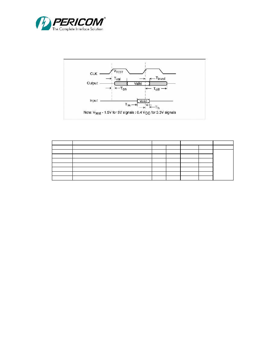
PI7C8148A
2-PORT PCI-TO-PCI BRIDGE
ADVANCE INFORMATION
Page 88 of 90
JUNE 2004 Revision 1.04
16.3 AC SPECIFICATIONS
Figure 16-1 PCI Signal Timing Measurement Conditions
66 MHz
33 MHz
Symbol Parameter
Min. Max. Min.
Max. Units
Tsu
Input setup time to CLK bused signals
1,2,3
3
-
7 -
Tsu(ptp)
Input setup time to CLK point-to-point
1,2,3
5
- 10,
12
4
-
Th
Input signal hold time from CLK
1,2
0
-
0
-
Tval
CLK to signal valid delay bused signals
1,2,3
2 6 2
11
Tval(ptp)
CLK to signal valid delay point-to-point
1,2,3
2 6 2
12
Ton
Float to active delay
1,2
2
-
2
-
Toff
Active to float delay
1,2
-
14
-
28
ns
1. See Figure 16-1 PCI Signal Timing Measurement Conditions.
2. All primary interface signals are synchronized to P_CLK. All secondary interface signals are
synchronized to S_CLKOUT.
3. Point-to-point signals are P_REQ#, S_REQ#[3:0], P_GNT#, S_GNT#[3:0], LOO, and ENUM#.
Bused signals are P_AD, P_CBE#, P_PAR, P_PERR#, P_SERR#, P_FRAME#, P_IRDY#, P_TRDY#,
P_LOCK#, P_DEVSEL#, P_STOP#, P_IDSEL, S_AD, S_CBE#, S_PAR, S_PERR#, S_SERR#,
S_FRAME#, S_IRDY#, S_TRDY#, S_LOCK#, S_DEVSEL#, and S_STOP#.
4. REQ# signals have a setup of 10ns and GNT# signals have a setup of 12ns.
PI7C8148A
2-PORT PCI-TO-PCI BRIDGE
ADVANCE INFORMATION
Page 89 of 90
JUNE 2004 Revision 1.04
16.4 66MHZ TIMING
Symbol Parameter
Condition
Min.
Max.
Units
T
SKEW
SKEW among S_CLKOUT[9:0]
0
0.250
T
DELAY
DELAY between PCLK and S_CLKOUT[9:0]
20pF load
2.63
3.78
T
CYCLE
P_CLK, S_CLKOUT[9:0] cycle time
15
30
T
HIGH
P_CLK, S_CLKOUT[9:0] HIGH time
6
T
LOW
P_CLK, S_CLKOUT[9:0] LOW time
6
ns
16.5 33MHZ TIMING
Symbol Parameter
Condition
Min.
Max.
Units
T
SKEW
SKEW among S_CLKOUT[9:0]
0
0.250
T
DELAY
DELAY between PCLK and S_CLKOUT[9:0]
20pF load
2.63
3.78
T
CYCLE
P_CLK, S_CLKOUT[9:0] cycle time
30
T
HIGH
P_CLK, S_CLKOUT[9:0] HIGH time
11
T
LOW
P_CLK, S_CLKOUT[9:0] LOW time
11
ns
16.6 POWER CONSUMPTION
Parameter Typical
Units
Power Consumption at 66MHz
769
mW
Supply Current, I
CC
233
mA
Note: Data taken at 25C and 3.3V V
CC
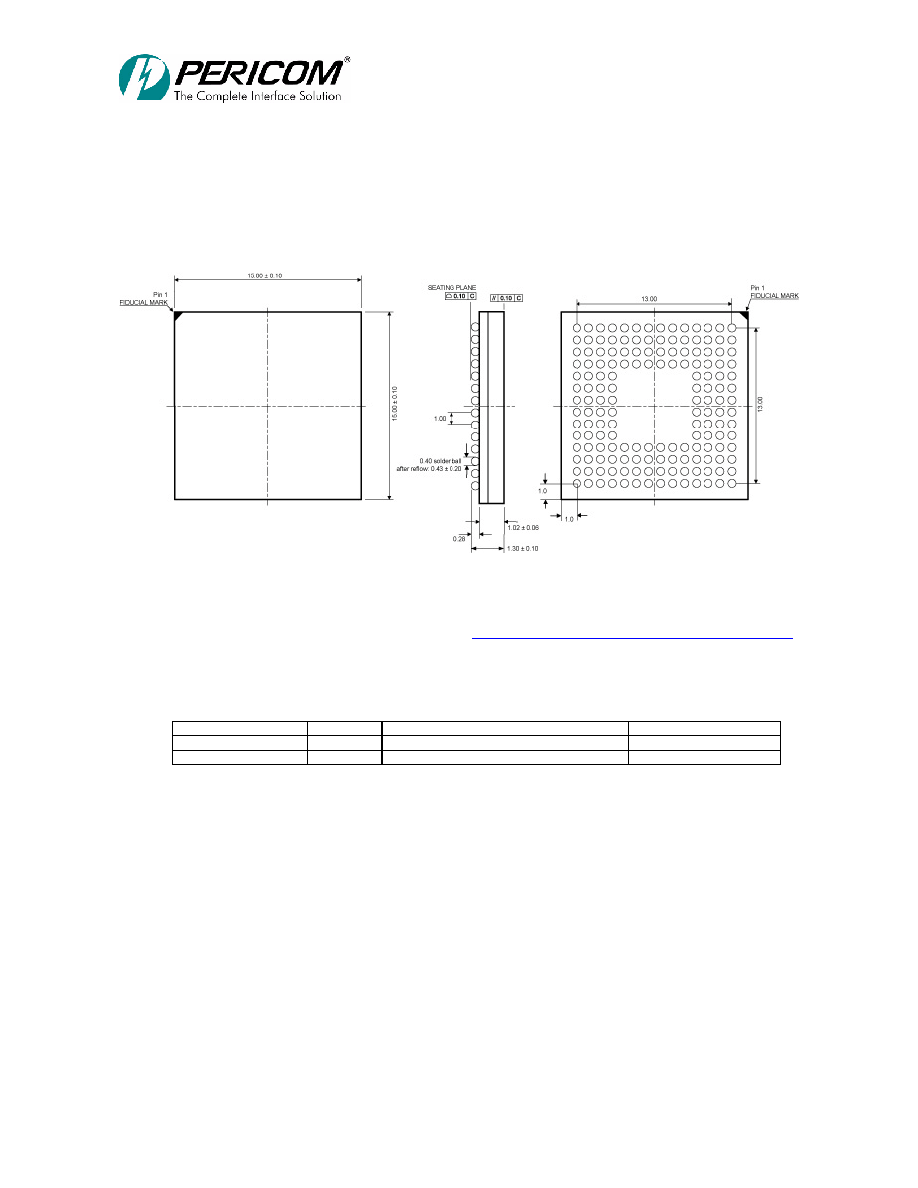
PI7C8148A
2-PORT PCI-TO-PCI BRIDGE
ADVANCE INFORMATION
Page 90 of 90
JUNE 2004 Revision 1.04
17 PACKAGE INFORMATION
17.1 160-PIN LFBGA PACKAGE OUTLINE
Figure 17-1 160-pin LFBGA package outline
Thermal characteristics can be found on the web:
http://www.pericom.com/packaging/mechanicals.php
17.2 PART NUMBER ORDERING INFORMATION
PART NUMBER
SPEED
PIN PACKAGE
TEMPERATURE
PI7C8148ANJ
66 MHz
160-pin LFBGA
0°C to 85°C
PI7C8148ANJE
66 MHz
160-pin LFBGA (Pb-free & Green)
0°C to 85°C