
1
PS8535C 10/04/04
V
CC
EN1
EN2
EN3
SEL
EN4
EN5
EN6
CEN
GND
CLK
SCLK
CLK
GND
D
CLK6
OUT≠
GND
CLK6
OUT+
16
15
17
13
14
11
12
9
8
7
6
5
4
3
2
1
10
CLK5
OUT≠
CLK5
OUT+
18
19
CLK4
OUT≠
CLK4
OUT+
20
21
CLK3
OUT≠
CLK3
OUT+
22
23
CLK2
OUT≠
CLK2
OUT+
24
25
CLK1
OUT≠
CLK1
OUT+
V
CC
26
27
28
Q
D
Q
D
Q
D
Q
D
Q
D
Q
1
0
PI90LVT211
Only 110
12345678901234567890123456789012123456789012345678901234567890121234567890123456789012345678901212345678901234567890123456789012123456789012
12345678901234567890123456789012123456789012345678901234567890121234567890123456789012345678901212345678901234567890123456789012123456789012
Features
∑ Meets or Exceeds Requirements of ANSI TIA/EIA-644-1995
∑ Designed for Clocking Rates up to 320MHz
∑ Operates from a single 3.3-V Supply
∑ Low-Voltage Differential Signaling (LVDS) with Output
Voltages of ±350mV into a 100-ohm load
∑ Choice between LVDS or TTL clock input
∑ Synchronous Enable/Disable
∑ Multiplexed clock input
≠ Internal 300 kohm pullup resistor on all control pins
≠ CLK and CLK have 110-ohm termination (PI90LVT211)
∑ Common and individual Enable/Disable control
∑ 50ps Output-to-Output Skew
∑ ±24ps Period Jitter
∑ Bus Pins are High Impedance when disabled or with V
CC
<1.5V
∑ TTL Inputs are 5V Tolerant
∑ Power Dissipation at 300 MHz
∑ P190LV211 is functionally compatible with Motorola's
(PECL) MC 10E211/MC100E211
∑ >12kV ESD Protection
∑ Packaging (Pb-free & Green available):
- 28-pin TSSOP (L)
- 28-pin QSOP (Q)
PI90LV211/PI90LVT211
Block Diagram & Pin Configuration
Description
The PI90LV211 implements low voltage differential signaling (LVDS)
to achieve clocking rates as high as 320 MHz with low skew. The
PI90LV211 is a low skew 1:6 fanout device designed explicitly for low
skew clock distribution applications. The device features a multi-
plexed clock input to allow for the distribution of a lower speed scan
or test clock with the high-speed system clock. When LOW the SEL
pin will select the differential clock input.
Both a common enable and individual output enables are provided.
When asserted the positive output will go LOW on the next negative
transition of the CLK (or SCLK) input. The enable function is
synchronous so that the outputs will only be enabled/disabled when
they are already in the LOW state. This avoids any chance of
generating a runt clock pulse when the device is enabled/disabled
as can happen with an asynchronous control. The internal flip flop
is clocked on the falling edge of the input clock, therefore all
associated specification limits are referenced to the negative edge
of the clock input.
Individual synchronous enable controls and multiplexed clock in-
puts make this device ideal as the first level distribution unit in a
distribution tree. The individual enables could be used to allow for the
disabling of individual cards on a backplane in fault tolerant designs.
K
L
C
/
K
L
C
K
L
C
S
L
E
S
x
N
E
N
E
C
)
±
(
T
U
O
K
L
C
L
/
H
X
X
L
/
H
L
H
X
H
L
L
H
L
L
L
L
H
K
L
C
K
L
C
S
*
Z
*
*
Z
Function Table
*
ENx disables individual banks
** CEN disables all six banks
= Negative transition of CLK or SCLK
Z = High Impedance
1:6 Differential Clock Distribution Chip

2
PS8535C 10/04/04
12345678901234567890123456789012123456789012345678901234567890121234567890123456789012345678901212345678901234567890123456789012123456789012
12345678901234567890123456789012123456789012345678901234567890121234567890123456789012345678901212345678901234567890123456789012123456789012
PI90LV211/PI90LVT211
1:6 Differential Clock
Distribution Chip
l
o
b
m
y
S
r
e
t
e
m
a
r
a
P
s
n
o
i
t
i
d
n
o
C
t
s
e
T
.
n
i
M
.
p
y
T
)
1
(
.
x
a
M
s
t
i
n
U
V
D
O
e
d
u
ti
n
g
a
m
e
g
a
tl
o
v
t
u
p
t
u
o
l
a
it
n
e
r
e
f
fi
D
R
L
0
0
1
=
2
d
n
a
1
s
e
r
u
g
i
F
e
e
S
7
4
2
0
4
3
4
5
4
V
m
V
D
O
e
g
a
tl
o
v
t
u
p
t
u
o
l
a
it
n
e
r
e
f
fi
d
n
i
e
g
n
a
h
C
s
e
t
a
t
s
c
i
g
o
l
n
e
e
w
t
e
b
e
d
u
ti
n
g
a
m
0
5
≠
0
5
V
)
S
S
(
C
O
t
u
p
t
u
o
e
d
o
m
-
n
o
m
m
o
c
e
t
a
t
s
-
y
d
a
e
t
S
e
g
a
tl
o
v
3
e
r
u
g
i
F
e
e
S
5
2
1
.
1
0
3
.
1
0
6
.
1
V
V
)
S
S
(
C
O
e
d
o
m
-
n
o
m
m
o
c
e
t
a
t
s
-
y
d
a
e
t
s
n
i
e
g
n
a
h
C
s
e
t
a
t
s
c
i
g
o
l
n
e
e
w
t
e
b
e
g
a
tl
o
v
t
u
p
t
u
o
0
5
≠
0
5
V
m
V
)
P
P
(
C
O
t
u
p
t
u
o
e
d
o
m
-
n
o
m
m
o
c
k
a
e
p
-
o
t
-
k
a
e
P
e
g
a
tl
o
v
0
4
0
5
1
I
C
C
t
n
e
r
r
u
C
y
l
p
p
u
S
R
,
d
e
l
b
a
n
E
L
0
0
1
=
V
N
I
V
=
C
C
D
N
G
r
o
7
2
5
3
A
m
V
,
d
e
l
b
a
s
i
D
N
I
V
=
C
C
D
N
G
r
o
0
.
3
9
.
3
I
H
I
t
n
e
r
r
u
c
t
u
p
n
i
l
e
v
e
l
-
h
g
i
H
V
H
I
V
2
=
8
.
4
0
2
A
µ
I
L
I
t
n
e
r
r
u
c
t
u
p
n
i
l
e
v
e
l
-
w
o
L
V
L
I
V
8
.
0
=
9
0
2
I
S
O
t
n
e
r
r
u
c
t
u
p
t
u
o
ti
u
c
ri
c
-
t
r
o
h
S
V
+
T
U
O
D
O
V
r
o
≠
T
U
O
D
O
V
0
=
7
±
A
m
V
D
O
V
0
=
5
.
4
±
I
Z
O
t
n
e
r
r
u
c
t
u
p
t
u
o
e
c
n
a
d
e
p
m
i
-
h
g
i
H
V
O
V
r
o
V
0
=
C
C
1
±
A
µ
I
)
F
F
O
(
O
t
n
e
r
r
u
c
t
u
p
t
u
o
f
f
o
-
r
e
w
o
P
V
C
C
V
,
V
1
.
1
=
O
V
4
.
2
=
1
±
C
N
I
,
e
c
n
a
ti
c
a
p
a
c
t
u
p
n
I
V
I
6
E
4
(
n
i
s
4
.
0
=
V
5
.
0
+
)
t
9
F
p
C
O
e
c
n
a
ti
c
a
p
a
c
t
u
p
t
u
O
V
I
6
E
4
(
n
i
s
4
.
0
=
d
e
l
b
a
s
i
D
,
V
5
.
0
+
)
t
0
1
R
M
R
E
T
r
o
t
s
i
s
e
R
n
o
it
a
n
i
m
r
e
T
1
1
2
T
V
L
0
9
I
P
0
9
0
1
1
2
3
1
Electrical Characteristics over Recommended Operating Conditions
(unless otherwise noted)
.

3
PS8535C 10/04/04
12345678901234567890123456789012123456789012345678901234567890121234567890123456789012345678901212345678901234567890123456789012123456789012
12345678901234567890123456789012123456789012345678901234567890121234567890123456789012345678901212345678901234567890123456789012123456789012
PI90LV211/PI90LVT211
1:6 Differential Clock
Distribution Chip
Notes:
1. Within-Device skew is defined for identical transitions on similar paths through a device.
2. Setup, Hold, and Disable times are all relative to a falling edge on CLK or SCLK.
3. Minimum input swing for which AC parameters are guaranteed. Full DC LVDS output swings will be generated with only 50mV input
swings.
4. The range in which the high level of the input swing must fall while meeting the V
PP
spec.
5. t
SKIR
is the difference in receiver propagation delay (t
PLH
-t
PHL
) of one device, and is the duty cycle distortion of the output at any given
temperature and V
CC
. The propagation delay specification is a device-to-device worst case over process, voltage, and temperature.
6. t
SK2R
is the difference in receiver propagation delay between channels in the same device of any outputs switching in the same direction. This
parameter is guaranteed by design and characterization.
7. Generator input conditions: t
r
t
f
< 1ns, 50% duty cycle, differential (1.10V to 1.35V peak-peak).
Output Criteria: 60%/40% duty cycle, V
OL
(max) 0-4V, V
OH
(min) 2.7V, Load - 7pF (stray plus probes).
8. C
L
includes probe and fixture capacitance.
9. Generator waveform for all tests unless otherwise specified: f = 25 MHz, Z
O
= 50 ohms, t
r
= 1ns, t
f
= 1ns (35%-65%). To ensure fastest propagation
delay and minimum skew, clock input edge rates should not be slower than 1ns/V; control signals not slower than 3ns/V.
Switching Characteristics over Recommended Operating Conditions
(unless otherwise noted)
(8,9)
.
c
i
t
s
i
r
e
t
c
a
r
a
h
C
l
o
b
m
y
S
.
n
i
M
.
p
y
T
.
x
a
M
s
t
i
n
U
n
o
i
t
i
d
n
o
C
t
u
p
t
u
O
o
t
y
a
l
e
D
n
o
i
t
a
g
a
p
o
r
P
±
T
U
O
K
L
C
o
t
K
L
C
±
T
U
O
K
L
C
o
t
K
L
C
S
±
T
U
O
K
L
C
o
t
L
E
S
t
H
L
P
t
L
H
P
5
.
1
5
.
1
5
.
1
7
.
2
7
.
2
7
.
2
4
.
3
4
2
.
3
6
.
3
s
n
e
m
i
T
e
l
b
a
s
i
D
±
T
U
O
K
L
C
o
t
K
L
C
S
r
o
K
L
C
t
Z
H
P
t
Z
L
P
t
H
Z
P
t
L
Z
P
2
.
2
1
.
2
6
.
3
8
.
2
8
.
2
8
.
2
8
.
4
8
.
4
2
w
e
k
S
t
r
a
P
-
o
t
-
t
r
a
P
Q
o
t
)
f
fi
D
(
K
L
C
Q
o
t
K
L
C
S
,
)
E
S
(
K
L
C
w
e
k
S
e
c
i
v
e
D
h
ti
W
t
w
e
k
s
D
B
T
D
B
T
D
B
T
s
p
1
r
e
t
t
i
J
e
l
c
y
C
-
o
t
-
e
l
c
y
C
t
)
c
c
(
ti
j
8
4
≠
8
4
+
6
e
r
u
g
i
F
r
e
t
t
i
J
d
o
i
r
e
P
t
)
r
e
p
(
ti
j
4
2
≠
4
2
+
7
e
r
u
g
i
F
e
m
i
T
p
u
t
e
S
x
N
E
K
L
C
o
t
K
L
C
o
t
N
E
C
t
s
0
0
2
0
0
2
0
0
1
≠
0
2
e
m
i
T
d
l
o
H
o
t
K
L
C
,
x
N
E
N
E
C
t
h
0
0
6
0
6
7
2
)
K
L
C
(
g
n
i
w
S
t
u
p
n
I
m
u
m
i
n
i
M
V
P
P
0
2
.
0
0
0
8
.
0
V
3
)
K
L
C
(
e
g
n
a
R
e
d
o
M
.
m
o
C
V
R
M
C
5
2
1
.
0
5
.
1
V
C
C
2
.
0
-
4
s
e
m
i
T
ll
a
F
/
e
s
i
R
%
0
8
≠
0
2
t
r
t
,
f
0
5
1
0
0
4
0
0
2
1
s
p
w
e
k
S
e
s
l
u
P
n
o
i
t
r
o
t
s
i
D
e
l
c
y
C
y
t
u
D
t
(
H
L
P
t
-
L
H
P
)
±
T
U
O
K
L
C
o
t
K
L
C
S
±
T
U
O
K
L
C
o
t
K
L
C
t
R
1
K
S
t
R
1
K
S
0
4
1
5
2
0
8
1
0
6
5
e
g
d
e
e
m
a
s
,
w
e
k
S
l
e
n
n
a
h
C
-
o
t
-
l
e
n
n
a
h
C
t
R
2
K
S
0
3
0
0
1
6
y
c
n
e
u
q
e
r
F
g
n
i
t
a
r
e
p
O
m
u
m
i
x
a
M
0
5
2
z
H
M
7
4
PS8535C 10/04/04
12345678901234567890123456789012123456789012345678901234567890121234567890123456789012345678901212345678901234567890123456789012123456789012
12345678901234567890123456789012123456789012345678901234567890121234567890123456789012345678901212345678901234567890123456789012123456789012
PI90LV211/PI90LVT211
1:6 Differential Clock
Distribution Chip
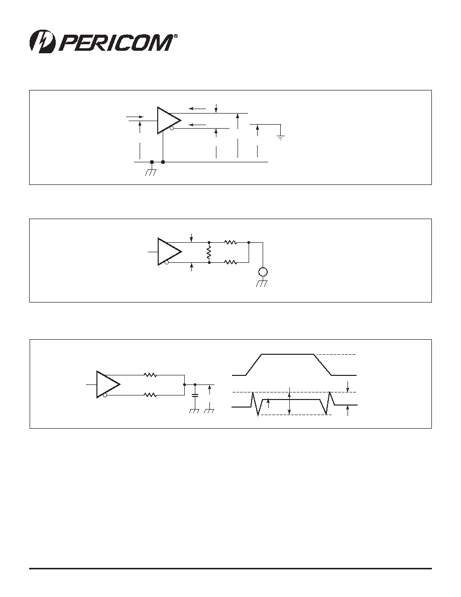
Figure 1. Voltage and Current Definitions
Parameter Measurement Information
Figure 2. V
OD
Test Circuit
Note:
1. All input pulses are supplied by a generator having the following characteristics: t
r
or t
f
1ns, Pulse Repetition Rate
(PRR) = 50 Mpps, Pulse width = 10 ±0.2ns. C
L
includes instrumentation and fixture capacitance within 0.06m of the D.U.T.
Themeasurement of VOC(PP) is made on test equipment with a ≠3dB bandwidth of at least 300MHz.
Figure 3. Test Circuit & Definitions for the Driver Common-Mode Output Voltage
D
IN
D
OUT+
D
OUT≠
V
ODOUT≠
V
ODOUT+
I
OY
GND
V
OD
V
I
V
OC
(V
ODOUT+
+V
ODOUT≠
)/2
I
I
I
OZ
Input
V
OD
100
3.75k
3.75k
0V
V
TEST
2.4V
±
D
OUT+
D
OUT≠
Input
3V
0V
V
I
V
OC
V
OC(PP)
V
OC(SS)
49.9
±1% (2 places)
D
OUT+
D
OUT≠

5
PS8535C 10/04/04
12345678901234567890123456789012123456789012345678901234567890121234567890123456789012345678901212345678901234567890123456789012123456789012
12345678901234567890123456789012123456789012345678901234567890121234567890123456789012345678901212345678901234567890123456789012123456789012
PI90LV211/PI90LVT211
1:6 Differential Clock
Distribution Chip
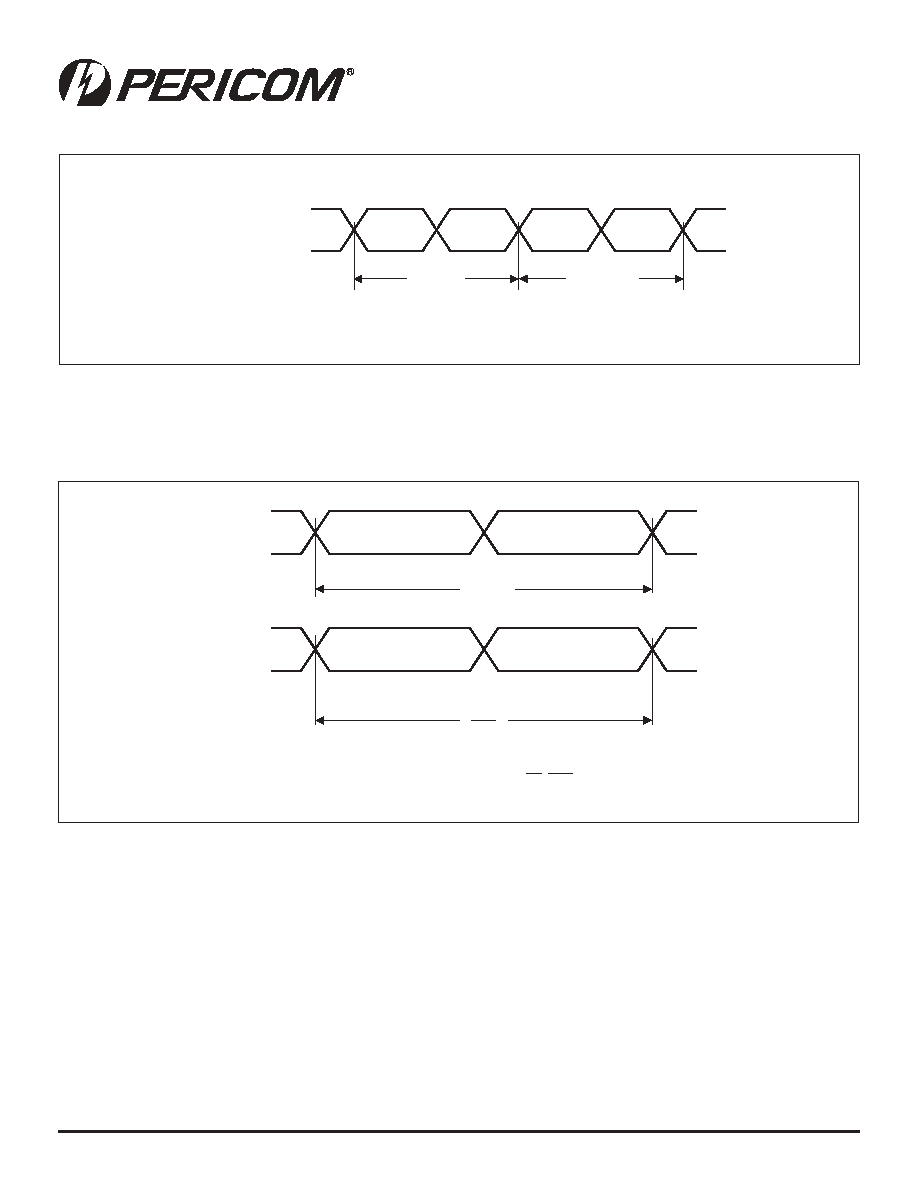
Figure 4. Test Circuit, Timing, & Voltage Definitions for the Differential Output Signal
Parameter Measurement Information (continued)
Note:
1. All input pulses are supplied by a generator having the following characteristics: t
r
or t
f
1ns, Pulse Repetition Rate
(PRR) = 15 Mpps, Pulse width = 10 ±0.2ns. C
L
includes instrumentation and fixture capacitance within 0.06m of the D.U.T.
Note:
1. All input pulses are supplied by a generator having the following characteristics: t
r
or t
f
1ns, Pulse Repetition Rate
(PRR) = 0.5 Mpps, Pulse width = 500 ±10ns. C
L
includes instrumentation and fixture capacitance within 0.06m of the D.U.T.
Figure 5. Enable & Disable Time Circuit & Definitions
Input
1.4V
32V
100%
80%
20%
0%
Input
Output
0V
V
OD
C
L
= 10pF
V
OD(H)
t
PLH
t
f
t
r
t
PHL
V
OD(L)
100
±1%
0.8V
(2 places)
D
OUT+
D
OUT≠
0.8V or 2V
Input
49.9
±1% (2 places)
1.2V
+
≠
1V
Input
2V
1.2V
1.1V
1.4V
0.8V
t
PZL
t
PLZ
1.2V
V
ODOUT+
or
V
ODOUT≠
V
ODOUT≠
or
V
ODOUT+
1.4V
1.3V
t
PZH
t
PHZ
D
OUT+
D
OUT≠
V
ODOUT+
V
ODOUT≠
6
PS8535C 10/04/04
12345678901234567890123456789012123456789012345678901234567890121234567890123456789012345678901212345678901234567890123456789012123456789012
12345678901234567890123456789012123456789012345678901234567890121234567890123456789012345678901212345678901234567890123456789012123456789012
PI90LV211/PI90LVT211
1:6 Differential Clock
Distribution Chip
Figure 6. Cycle-to-Cycle Jitter
Figure 7. Period Jitter
C L KO U T ≠
C L KO U T +
C L KO U T ≠
C L KO U T +
t
cycle n
f
O
1
t
jit(per)
=
t
cycle n
f
O
1
t
jit(cc)
=
t
cycle n
-
t
cycle n+1
t
cycle n+1
t
cycle n
C L KO U T ≠
C L KO U T +
7
PS8535C 10/04/04
12345678901234567890123456789012123456789012345678901234567890121234567890123456789012345678901212345678901234567890123456789012123456789012
12345678901234567890123456789012123456789012345678901234567890121234567890123456789012345678901212345678901234567890123456789012123456789012
PI90LV211/PI90LVT211
1:6 Differential Clock
Distribution Chip
General Desciption
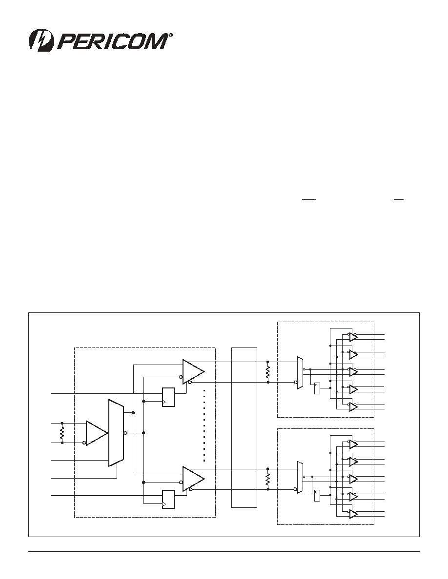
The PI90LV211 is a 1:6 fanout tree designed explicitly for low-skew,
high-speed clock distribution. The device was targeted to work in
conjunction with the PI90LV14 device to provide another level of
flexibility in the design and implementation of clock distribution
trees. The individual synchronous enable controls and multiplexed
clock inputs make the device ideal as the first level distribution unit
in a distribution tree. The device provides the ability to distribute
a lower speed scan or test clock along with the high-speed system
clock to ease the design of system diagnostics and self test
procedures. The individual enables could be used to allow for the
disabling of individual cards on a backplane in fault tolerant
designs.
Handling Open Inputs and Outputs
With the simultaneous switching characteristics and the tight skew
specifications of the P90LV211, the handling of the unused outputs
becomes critical. To minimize the noise generated on the die
all outputs should be terminated in pairs, i.e. both the true and
compliment outputs should be terminated even if only one of the
outputs will be used in the system. With both complimentary pairs
terminated, the current in the V
CC
pins will remain essentially
constant and thus inductance induced voltage glitches on V
CC
will
not occur. V
CC
glitches will result in distorted output waveforms
and degradations in the skew performance of the device.
The package parasitics of the 28-lead package cause the signals on
a given pin to be influenced by signals on adjacent pins. PI90LV211
is characterized and tested with all of the outputs switching,
therefore the numbers in the data book are guaranteed only for this
situation. If all of the outputs of the PI90LV211 are not needed and
there is a desire to save power, the unused output pairs can be left
unterminated. Unterminated outputs can influence the propagation
delay on adjacent pins by 15ps≠20ps. Therefore, under these
conditions, this 15ps≠20ps needs to be added to the overall skew
of the device. Pins which are separated by a package corner are not
considered adjacent pins in the context of propagation delay
influence. Therefore if all of the outputs on a single side of the
package are terminated, the specification limits in the data sheet will
apply.
Using the Enable Pins
Both the common enable (CEN) and the individual enables (ENx) are
synchronous to the CLK or SCLK input depending on which is
selected. The active low signals are clocked into the enable flip flops
on the negative edges of the PI90LV211 clock inputs. In this way,
the devices will only be disabled when the outputs are already in the
LOW state. The internal propagation delays are such that the delay
to the output through the distribution buffers is less than that
through the enable flip flops. This will ensure that the disabling of
the device will not slice any time off the clock pulse. On initial power
up, the enable flip flops will randomly attain a stable state; therefore
precautions should be taken on initial power up to ensure the
PI90LV211 is in the desired state.
Figure 8. Standard PI90LV211 LVDS Application
B
A
CKPLANE
PI90LV14
PI90LV211
D0
D5
PI90LV14

8
PS8535C 10/04/04
12345678901234567890123456789012123456789012345678901234567890121234567890123456789012345678901212345678901234567890123456789012123456789012
12345678901234567890123456789012123456789012345678901234567890121234567890123456789012345678901212345678901234567890123456789012123456789012
PI90LV211/PI90LVT211
1:6 Differential Clock
Distribution Chip
Packaging Mechanical: 28-Pin QSOP (Q)
Packaging Mechanical: 28-Pin TSSOP (L)
.378
.386
.047
1.20
.002
.006
SEATING
PLANE
.0256
BSC
.018
.030
.252
BSC
1
28
.169
.177
X.XX
X.XX
DENOTES CONTROLLING
DIMENSIONS IN MILLIMETERS
0.05
0.15
6.4
0.45
0.75
0.09
0.20
4.3
4.5
9.6
9.8
0.65
0.19
0.30
.007
.012
.004
.008
Max
.386
.394
.053
.069
.004
.010
SEATING
PLANE
.025
BSC
.007
.010
.228
.244
0.150
0.157
1
28
.016
.050
X.XX
X.XX
DENOTES DIMENSIONS
IN MILLIMETERS
0.635
9.804
10.009
1.35
1.75
5.79
6.19
0.41
1.27
0.101
0.254
.008
.012
0.203
0.305
3.81
3.99
0.178
0.254
.033
0.84
.015 x 45∞
REF
Detail A
Detail A
.008
0.20
MIN.
Guage Plane
.010
0.254
.041
1.04
REF
.016
.035
0.41
0.89
0∞-6∞
.008
.013
0.20
0.33

9
PS8535C 10/04/04
12345678901234567890123456789012123456789012345678901234567890121234567890123456789012345678901212345678901234567890123456789012123456789012
12345678901234567890123456789012123456789012345678901234567890121234567890123456789012345678901212345678901234567890123456789012123456789012
PI90LV211/PI90LVT211
1:6 Differential Clock
Distribution Chip
Notes:
1. Thermal characteristics can be found on the company web site at www.pericom.com/packaging/
Ordering Information
Ordering Code
Package Code
Package Type
PI90LV211L
L
28-pin 173-mil TSSOP
PI90LV211LE
L
Pb-free & Green, 28-pin 173-mil TSSOP
PI90LV211Q
Q
28-pin 150-mil QSOP
PI90LV211QE
Q
Pb-free & Green, 28-pin 150-mil QSOP
PI90LVT211L
L
28-pin 173-mil TSSOP
PI90LVT211LE
L
Pb-free & Green, 28-pin 173-mil TSSOP
PI90LVT211Q
Q
28-pin 150-mil QSOP
PI90LVT211QE
Q
Pb-free & Green, 28-pin 150-mil QSOP