1
PS8667A 10/04/04
12345678901234567890123456789012123456789012345678901234567890121234567890123456789012345678901212345678901234567890123456789012123456789012
12345678901234567890123456789012123456789012345678901234567890121234567890123456789012345678901212345678901234567890123456789012123456789012
LVDS High-Speed Differential
Line Receivers
Features
∑ Signaling Rates >400Mbps (200 MHz)
∑ Single 3.3V Power Supply Design
∑ Accepts ±350mV (typical) Differential Swing
∑ Maximum Differential Skew of 0.35ns
∑ Integrated 110-Ohm termination on PI90LVTxxxx
∑ Maximum Propagation Delay of 4.7ns
∑ Low Voltage TTL (LVTTL) Outputs
∑ Industrial Temperature Operating Range: -40∞C to 85∞C
∑ Open, Short, and Terminated Fail Safe
∑ Meets or Exceeds ANSI/TIA/EIA-644 LVDS Standard
∑ Packaging (Pb-free & Green available):
-16-Pin TSSOP (L )
-16-Pin SOIC (W)
-8-Pin SOIC (W)
-8-Pin MSOP (U)
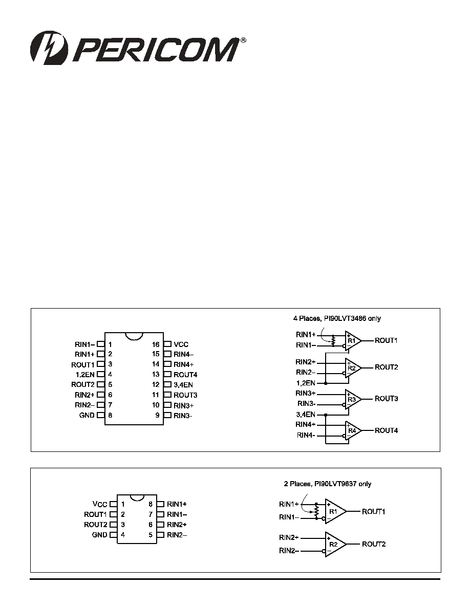
PI90LV/LVT3486
PI90LV/LVT9637
PI90LV3486/PI90LVT3486
PI90LV9637/PI90LVT9637
Description
The PI90LV/LVT3486 and PI90LV/LVT9637 are differential line
receivers that use low-voltage differential signaling (LVDS) to
support data rates in excess of 400 Mbps. These products are
designed for applications requiring high-speed, low-power con-
sumption and low noise generation.
A differential input signal (350mV) is translated by the device to 3V
CMOS output level.
Applications
Applications include point-to-point and multidrop baseband data
transmission over controlled impedance media of approximately
100-ohms. The transmission media can be printed circuit board
traces, backplanes, or cables.
The PI90LV/LVT3486 and PI90LV/LVT9637, as well as companion
line drivers PI90LV/LVB3487 and PI90LV/LVB9638 provide new
alternatives to RS-232, PECL, and ECL devices for high-speed,
point-to-point interface applications.
16-Pin
W, L
8-Pin
W,U
2
PS8667A 10/04/04
12345678901234567890123456789012123456789012345678901234567890121234567890123456789012345678901212345678901234567890123456789012123456789012
12345678901234567890123456789012123456789012345678901234567890121234567890123456789012345678901212345678901234567890123456789012123456789012
PI90LV3486/PI90LVT3486
PI90LV9637/PI90LVT9637
LVDS High-Speed Differential Line Receivers
Function Tables
Pin Descriptions
e
l
b
a
n
E
s
t
u
p
n
I
l
a
i
t
n
e
r
e
f
f
i
D
t
u
p
t
u
O
N
E
R
+
N
I
R
,
≠
N
I
R
T
U
O
H
V
D
I
V
m
0
0
1
H
H
V
<
V
m
0
0
1
≠
D
I
V
m
0
0
1
<
?
H
V
D
I
V
m
0
0
1
≠
L
L
X
Z
H
n
e
p
O
H
PI90LV/LVT3486
PI90LV/LVT9637
s
t
u
p
n
I
l
a
i
t
n
e
r
e
f
f
i
D
t
u
p
t
u
O
R
+
N
I
R
,
≠
N
I
R
T
U
O
V
D
I
V
m
0
0
1
H
V
<
V
m
0
0
1
≠
D
I
V
m
0
0
1
<
?
V
D
I
V
m
0
0
1
≠
L
n
e
p
O
H
e
m
a
N
n
o
i
t
p
i
r
c
s
e
D
R
T
U
O
s
n
i
p
t
u
p
t
u
o
r
e
v
i
e
c
e
r
S
O
M
C
/
L
T
T
R
+
N
I
s
n
i
p
t
u
p
n
i
r
e
v
i
e
c
e
r
g
n
it
r
e
v
n
i
-
n
o
N
R
≠
N
I
s
n
i
p
t
u
p
n
i
r
e
v
i
e
c
e
r
g
n
it
r
e
v
n
I
D
N
G
n
i
p
d
n
u
o
r
G
V
C
C
%
0
1
±
V
3
.
3
+
,
n
i
p
y
l
p
p
u
s
r
e
w
o
p
e
v
it
i
s
o
P
Supply Voltage (V
CC
) ....................................... ≠0.3V to +4.0V
Input Voltage (R
IN+
, R
IN-
) ............................... ≠0.3V to +3.9V
Enable Input Voltage (EN) ...................... ≠0.3V to (V
CC
+0.3V)
Output Voltage (R
OUT
) .......................... ≠0.3V to (V
CC
+0.3V)
S Package .................................................................... 750mW
Derate S Package ................................8.2mW/∞C above +25∞C
Storage Temperature Range .......................... ≠65∞C to +150∞C
Lead Temperature Range Soldering (4s) ...................... +260∞C
Maximum Junction Temperature .................................. +150∞C
ESD Rating ...................................................................
10kV
Note:
Stresses greater than those listed under Absolute Maximum Ratings may
cause permanent damage to the device. This is a stress rating only and
functional operation of the device at these or any other conditions above
those indicated in the operational sections of this specification is not
implied. Exposure to absolute maximum rating conditions for extended
periods may affect reliability.
Absolute Maximum Ratings
(see Note 1, Page 4)
Recommended Operating Conditions
.
n
i
M
.
p
y
T
.
x
a
M
s
t
i
n
U
V
(
e
g
a
tl
o
V
y
l
p
p
u
S
C
C
)
0
.
3
+
3
.
3
+
6
.
3
+
V
e
g
a
tl
o
V
t
u
p
n
I
r
e
v
i
e
c
e
R
D
N
G
0
.
3
+
ri
A
e
e
r
F
g
n
it
a
r
e
p
O
T
(
e
r
u
t
a
r
e
p
m
e
T
A
)
0
4
≠
5
2
+
5
8
+
C
∞

3
PS8667A 10/04/04
12345678901234567890123456789012123456789012345678901234567890121234567890123456789012345678901212345678901234567890123456789012123456789012
12345678901234567890123456789012123456789012345678901234567890121234567890123456789012345678901212345678901234567890123456789012123456789012
PI90LV3486/PI90LVT3486
PI90LV9637/PI90LVT9637
LVDS High-Speed Differential Line Receivers
l
o
b
m
y
S
r
e
t
e
m
a
r
a
P
s
n
o
i
t
i
d
n
o
C
n
i
P
.
n
i
M
.
p
y
T
.
x
a
M
s
t
i
n
U
V
H
T
h
g
i
H
t
u
p
n
I
l
a
it
n
e
r
e
f
fi
D
d
l
o
h
s
e
r
h
T
V
2
.
1
+
=
m
c
V
)
2
1
(
R
+
N
I
,
R
-
N
I
0
2
+
0
0
1
+
V
m
V
L
T
w
o
L
t
u
p
n
I
l
a
it
n
e
r
e
f
fi
D
d
l
o
h
s
e
r
h
T
0
0
1
≠
0
2
≠
R
M
C
V
e
g
a
tl
o
V
e
d
o
M
-
n
o
m
m
o
C
e
g
n
a
R
V
D
I
k
a
e
p
-
o
t
-
k
a
e
p
V
m
0
0
2
=
)
5
(
1
.
0
6
.
2
V
I
N
I
t
n
e
r
r
u
C
t
u
p
n
I
V
N
I
V
8
.
2
+
=
V
C
C
V
0
r
o
6
.
3
+
=
0
1
≠
1
±
0
1
+
A
µ
V
N
I
V
0
=
0
1
≠
1
±
0
1
+
V
N
I
V
6
.
3
+
=
V
C
C
V
0
=
0
2
≠
0
2
+
V
H
O
e
g
a
tl
o
V
h
g
i
H
t
u
p
t
u
O
I
H
O
V
,
A
m
4
.
0
≠
=
D
I
V
m
0
0
2
+
=
R
T
U
O
7
.
2
0
.
3
V
I
H
O
d
e
t
a
n
i
m
r
e
t
t
u
p
n
I
,
A
m
4
.
0
≠
=
7
.
2
0
.
3
I
H
O
d
e
t
r
o
h
s
t
u
p
n
I
,
A
m
4
.
0
≠
=
7
.
2
0
.
3
V
L
O
e
g
a
tl
o
V
w
o
L
t
u
p
t
u
O
I
L
O
V
,
A
m
2
=
D
I
V
m
0
0
2
≠
=
1
.
0
5
2
.
0
I
S
O
t
n
e
r
r
u
C
ti
u
c
ri
C
t
r
o
h
S
t
u
p
t
u
O
V
0
=
t
u
o
V
,
d
e
l
b
a
n
E
)
0
1
(
5
1
≠
8
4
≠
0
2
1
≠
A
m
I
Z
O
t
n
e
r
r
u
C
e
t
a
t
S
-
e
e
r
h
T
t
u
p
t
u
O
V
,
d
e
l
b
a
s
i
D
T
U
O
V
r
o
V
0
=
C
C
0
1
≠
1
±
0
1
+
A
µ
V
H
I
e
g
a
tl
o
V
h
g
i
H
t
u
p
n
I
N
E
0
.
2
V
C
C
V
V
L
I
e
g
a
tl
o
V
w
o
L
t
u
p
n
I
D
N
G
8
.
0
I
I
t
n
e
r
r
u
C
t
u
p
n
I
V
N
I
V
r
o
V
0
=
C
C
V
=
t
u
p
n
I
r
e
h
t
O
,
C
C
D
N
G
r
o
0
2
≠
1
±
0
2
+
A
µ
V
L
C
e
g
a
tl
o
V
p
m
a
l
C
t
u
p
n
I
I
L
C
A
m
8
1
≠
=
5
.
1
≠
8
.
0
≠
V
I
C
C
t
n
e
r
r
u
C
y
l
p
p
u
S
d
a
o
L
o
N
d
e
l
b
a
n
E
s
r
e
v
i
e
c
e
R
V
=
N
E
C
C
n
e
p
O
s
t
u
p
n
I
,
D
N
G
r
o
V
C
C
0
1
5
1
A
m
n
e
p
O
s
t
u
p
n
I
,
V
5
.
0
r
o
V
4
.
2
=
N
E
0
1
5
1
I
Z
C
C
t
n
e
r
r
u
C
y
l
p
p
u
S
d
a
o
L
o
N
d
e
l
b
a
s
i
D
s
r
e
v
i
e
c
e
R
n
e
p
O
s
t
u
p
n
I
,
D
N
G
=
N
E
7
0
1
C
W
e
c
n
a
ti
c
a
p
a
C
t
u
p
n
I
5
0
1
F
p
R
M
R
E
T
e
c
n
a
d
e
p
m
I
n
o
it
a
n
i
m
r
e
T
x
x
x
x
T
V
L
0
9
I
P
0
9
0
1
1
3
4
1
Electrical Characteristics
Over supply voltage and operating temperature ranges, unless otherwise specified. (Note 2)
4
PS8667A 10/04/04
12345678901234567890123456789012123456789012345678901234567890121234567890123456789012345678901212345678901234567890123456789012123456789012
12345678901234567890123456789012123456789012345678901234567890121234567890123456789012345678901212345678901234567890123456789012123456789012
PI90LV3486/PI90LVT3486
PI90LV9637/PI90LVT9637
LVDS High-Speed Differential Line Receivers
Switching Characteristics
Over supply voltage and operating temperature ranges, unless otherwise specified. (Notes 3,4,7,8)
l
o
b
m
y
S
r
e
t
e
m
a
r
a
P
s
n
o
i
t
i
d
n
o
C
.
n
i
M
.
p
y
T
.
x
a
M
s
t
i
n
U
t
D
L
H
P
V
(
w
o
L
o
t
h
g
i
H
y
a
l
e
D
n
o
it
a
g
a
p
o
r
P
l
a
it
n
e
r
e
f
fi
D
M
C
)
V
3
2
.
1
=
C
L
F
p
0
1
=
V
D
I
V
m
0
0
2
=
)
2
&
1
s
e
r
u
g
i
F
(
8
.
1
7
.
4
s
n
t
D
H
L
P
V
(
h
g
i
H
o
t
w
o
L
y
a
l
e
D
n
o
it
a
g
a
p
o
r
P
l
a
it
n
e
r
e
f
fi
D
M
C
)
V
3
2
.
1
=
8
.
1
7
.
4
t
1
D
K
S
t
|
w
e
k
S
e
s
l
u
P
l
a
it
n
e
r
e
f
fi
D
D
L
H
P
t
-
D
H
L
P
|
)
6
(
0
1
.
0
5
.
0
t
2
D
K
S
e
c
i
v
e
d
e
m
a
s
-
w
e
k
S
l
e
n
n
a
h
C
-
o
t
-l
e
n
n
a
h
C
l
a
it
n
e
r
e
f
fi
D
)
7
(
0
1
.
0
5
.
0
t
3
D
K
S
w
e
k
S
t
r
a
P
-
o
t
-
t
r
a
P
l
a
it
n
e
r
e
f
fi
D
)
8
(
0
.
1
t
4
D
K
S
w
e
k
S
t
r
a
P
-
o
t
-
t
r
a
P
l
a
it
n
e
r
e
f
fi
D
)
9
(
5
.
1
t
H
L
T
e
m
i
T
e
s
i
R
5
3
.
0
2
.
1
t
L
H
T
e
m
i
T
ll
a
F
5
3
.
0
2
.
1
t
Z
H
P
Z
o
t
h
g
i
H
e
m
i
T
e
l
b
a
s
i
D
R
L
k
2
=
8
2
1
t
Z
L
P
Z
o
t
w
o
L
e
m
i
T
e
l
b
a
s
i
D
C
L
F
p
0
1
=
)
4
&
3
s
e
r
u
g
i
F
(
6
2
1
t
H
Z
P
h
g
i
H
o
t
Z
e
m
i
T
e
l
b
a
n
E
1
1
7
1
t
L
Z
P
w
o
L
o
t
Z
e
m
i
T
e
l
b
a
n
E
1
1
7
1
f
X
A
M
y
c
n
e
u
q
e
r
F
g
n
it
a
r
e
p
O
m
u
m
i
x
a
M
)
3
1
(
g
n
i
h
c
ti
w
s
s
l
e
n
n
a
h
c
ll
A
0
5
2
z
H
M
Notes:
1.
"Absolute Maximum Ratings" are those values beyond which the safety of the device cannot be guaranteed. They are not meant to imply
that the devices should be operated at these limits. The table of "Electrical Characteristics" specifies conditions of device operation.
2.
Current into device pins is defined as positive. Current out of device pins is defined as negative. All voltages are referenced to ground unless
otherwise specified.
3.
All typicals are given for: V
CC
= +3.3V, T
A
= +25∞C.
4.
Generator waveform for all tests unless otherwise specified: f = 1 MHz, Z
O
= 50
,
t
R
and t
F
(0% to 100%)
3
ns for R
IN
.
5.
The VCMR range is reduced for larger V
ID
. Example : if V
ID
= 400mV, the VCMR is 0.2V to 2.2V. The fail-safe condition with inputs
shorted is valid over a common-mode range of 0V to 2.3V. A V
ID
up tp V
CC
- 0V may be applied to the R
IN+
/ R
IN-
inputs with the
Common-Mode voltage set to V
CC
/2. Propagation delay and Differential Pulse skew decrease when VID is increased from 200mV to
400mV. Skew specifications apply for 200mV
V
ID
800mV over the common mode range.
6.
tskd1 is the magnitude difference in differential propagation delay time between the positive going edge and the negative going edge of the
same channel.
7.
t
SKD2
, Channel-to-Channel Skew, is defined as the difference between the propagation delay of one channel and that of the others on the
same chip with any event on the inputs.
8.
t
SKD3
, Part-to-Part Skew, is the differential Channel-to-Channel skew of any event between devices. This specification applies to devices
at the same V
CC
,and within 5∫C of each other within the operating temperature range.
9.
t
SKD4
, Part-to-Part Skew, is the differential Channel-to-Channel skew of any event between devices. This specification applies
to devices over recommended operating temperature and voltage ranges, and across process distribution. tskd4 is defined as IMax - Mini
differential propagation delay.
10. Output short circuit current (I
OS
) is specified as magnitude only, minus sign indicates direction only. Only one output should be shorted at
a time, do not exceed maximum junction temperature specification.
11. C
L
includes probe and jig capacitance.
12. V
CC
is always higher than R
IN+
and R
IN-
voltage. R
IN-
and R
IN+
are allowed to have a voltage range -0.2V to V
CC
- V
ID
/2.
However, to be compliant with AC specifications, the common voltage range 0.1V to 2.3V.
13. fmax generator input conditions: t
R
= t
F
< 1ns, (0% to 100%), 50% duty cycle, differential (1.05V to1.35V peak to peak).
Output Criteria: duty cycle = 60%/40%, V
OL
(max 0.4V), V
OH
(min 2.7V), Load = 10pF (stray plus probes).
5
PS8667A 10/04/04
12345678901234567890123456789012123456789012345678901234567890121234567890123456789012345678901212345678901234567890123456789012123456789012
12345678901234567890123456789012123456789012345678901234567890121234567890123456789012345678901212345678901234567890123456789012123456789012
PI90LV3486/PI90LVT3486
PI90LV9637/PI90LVT9637
LVDS High-Speed Differential Line Receivers
EN
Generator
R
OUT
R
L
R
IN+
R
IN≠
50
C
L
S
1
V
CC
Device
Under
Test
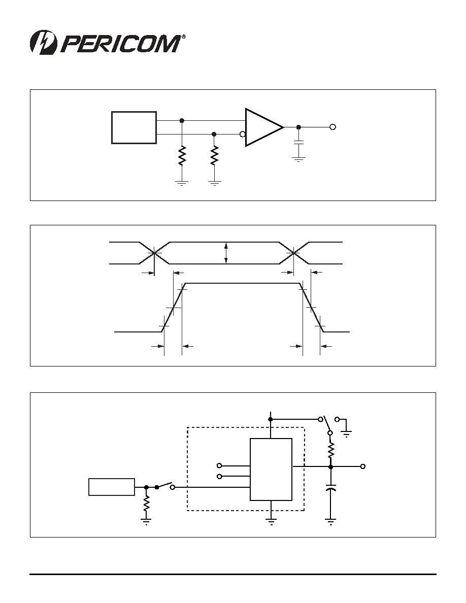
Parameter Measurement Information
Figure 1. Receiver Propagation Delay and Transition Time Test Circuit
Figure 2. Receiver Propagation Delay and Transition Time Waveforms
Generator
Receiver Enabled
RIN+
ROUT
R
RIN≠
CL
50
50
t
TLH
20%
R
OUT
V
ID =
200mV
R
IN-
R
IN+
V
OL
t
PHLD
t
PLHD
+1.3V
+1.1V
1.5V
0V (Differential)
+1.2V
1.5V
80%
80%
20%
t
THL
Figure 3. Receiver Three-State Delay Test Circuit
C
L
includes load and test jig capacitance.
S
1
= V
CC
for T
PZL
, and T
PLZ
measurements
S
1
= GND for t
PZH
and t
PHZ
measurements

6
PS8667A 10/04/04
12345678901234567890123456789012123456789012345678901234567890121234567890123456789012345678901212345678901234567890123456789012123456789012
12345678901234567890123456789012123456789012345678901234567890121234567890123456789012345678901212345678901234567890123456789012123456789012
PI90LV3486/PI90LVT3486
PI90LV9637/PI90LVT9637
LVDS High-Speed Differential Line Receivers
Figure 4. Receiver Three-State Delay Waveforms
Output When
V
ID
= +100mV
Output When
V
ID
= -100mV
EN* When EN = GND
EN When EN* = V
CC
3V
0V
0.5V
0.5V
50%
50%
1.5V
1.5V
1.5V
1.5V
t
PZL
t
PZH
V
CC
GND
t
PLZ
t
PHZ
0V
3V
V
OH
V
OL
Figure 5. Point-to-Point Application
ANY LVDS DRIVER
Enable
Data
Input
1/4 PI90LV3486
Data
Output
RT
+
≠
100
Balanced System

7
PS8667A 10/04/04
12345678901234567890123456789012123456789012345678901234567890121234567890123456789012345678901212345678901234567890123456789012123456789012
12345678901234567890123456789012123456789012345678901234567890121234567890123456789012345678901212345678901234567890123456789012123456789012
PI90LV3486/PI90LVT3486
PI90LV9637/PI90LVT9637
LVDS High-Speed Differential Line Receivers
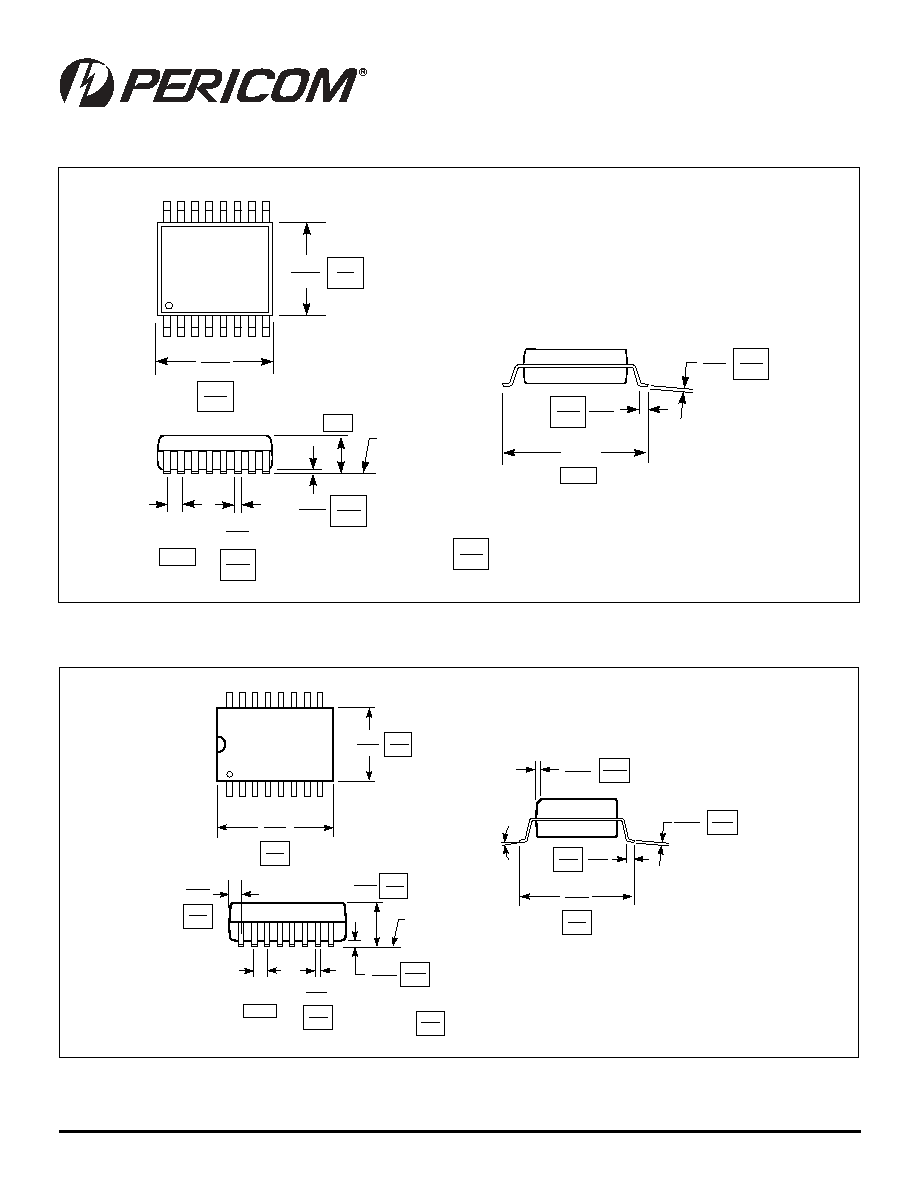
Packaging Mechanical: 16-Pin MSOP (U)
.0040
.0098
SEATING PLANE
.013
.020
.050
BSC
.016
.0075
.0098
1
8
.0099
.0196
0-8∞
.050
.149
.157
X.XX
X.XX
DENOTES DIMENSIONS
IN MILLIMETERS
3.78
3.99
.189
.196
4.80
5.00
1.27
.016
.026
1.35
1.75
.2284
.2440
5.80
6.20
0.406
0.660
0.330
0.508
0.10
0.25
0.40
1.27
0.19
0.25
0.25
0.50
x 45∞
.053
.068
REF
Packaging Mechanical: 8-Pin SOIC (W)
15
∞
MAX
15
∞
MAX
Detail A
Detail A
.112
.120
2.85
3.05
.114
.122
2.90
3.10
.114
.122
2.90
3.10
.010
0
∞
- 6
∞
15∞ Max.
15∞ Max.
0.25
Gauge
Plane
.003
.012
.016
.028
.037
0.40
0.70
0.95
REF
0.07
0.30
.003
.012
0.07
0.30
8
PS8667A 10/04/04
12345678901234567890123456789012123456789012345678901234567890121234567890123456789012345678901212345678901234567890123456789012123456789012
12345678901234567890123456789012123456789012345678901234567890121234567890123456789012345678901212345678901234567890123456789012123456789012
PI90LV3486/PI90LVT3486
PI90LV9637/PI90LVT9637
LVDS High-Speed Differential Line Receivers
Packaging Mechanical: 16-Pin TSSOP (L)
.193
.201
.047
max.
.002
.006
SEATING
PLANE
.0256
BSC
.018
.030
.004
.008
.252
BSC
1
16
.169
.177
X.XX
X.XX
DENOTES CONTROLLING
DIMENSIONS IN MILLIMETERS
0.05
0.15
6.4
0.45
0.75
0.09
0.20
4.3
4.5
1.20
4.9
5.1
0.65
0.19
0.30
.007
.012
SEATING PLANE
.050
BSC
1
16
0-8∞
.149
.157
X.XX
X.XX
DENOTES DIMENSIONS
IN MILLIMETERS
3.78
3.99
.386
.393
9.80
10.00
1.27
.053
.068
1.35
1.75
.2284
.2440
5.80
6.20
.0040
.0098
0.10
0.25
.013
.020
.0155
.0260
0.330
0.508
0.393
0.660
.0075
.0098
0.25
0.50
.0099
.0196
x 45∞
0.19
0.25
.016
.050
0.41
1.27
REF
Packaging Mechanical: 16-Pin SOIC (W)

9
PS8667A 10/04/04
12345678901234567890123456789012123456789012345678901234567890121234567890123456789012345678901212345678901234567890123456789012123456789012
12345678901234567890123456789012123456789012345678901234567890121234567890123456789012345678901212345678901234567890123456789012123456789012
PI90LV3486/PI90LVT3486
PI90LV9637/PI90LVT9637
LVDS High-Speed Differential Line Receivers
Pericom Semiconductor Corporation ∑ 1-800-435-2336 ∑ www.pericom.com
Notes:
1. Thermal characteristics can be found on the company web site at www.pericom.com/packaging/
Ordering Information
Ordering Code
Package Code
Package Type
PI90LV3486L
L
16-pin TSSOP
PI90LV3486LE
L
Pb-free & Green, 16-pin TSSOP
PI90LV3486W
W
16-pin SOIC
PI90LV3486WE
W
Pb-free & Green, 16-pin SOIC
PI90LVT3486L
L
16-pin TSSOP
PI90LVT3486LE
L
Pb-free & Green, 16-pin TSSOP
PI90LVT3486W
W
16-pin SOIC
PI90LVT3486WE
W
Pb-free & Green, 16-pin SOIC
PI90LV9637U
U
8-pin MSOP
PI90LV9637UE
U
Pb-free & Green, 8-pin MSOP
PI90LV9637W
W
8-pin SOIC
PI90LV9637WE
W
Pb-free & Green, 8-pin SOIC
PI90LVT9637U
U
8-pin MSOP
PI90LVT9637UE
U
Pb-free & Green, 8-pin MSOP
PI90LVT9637W
W
8-pin SOIC
PI90LVT9637WE
W
Pb-free & Green, 8-pin SOIC