
1
PS8540A 08/07/01
12345678901234567890123456789012123456789012345678901234567890121234567890123456789012345678901212345678901234567890123456789012123456789012
12345678901234567890123456789012123456789012345678901234567890121234567890123456789012345678901212345678901234567890123456789012123456789012
PI90LVB179/PI90LVB180/
PI90LVB050/PI90LVB051
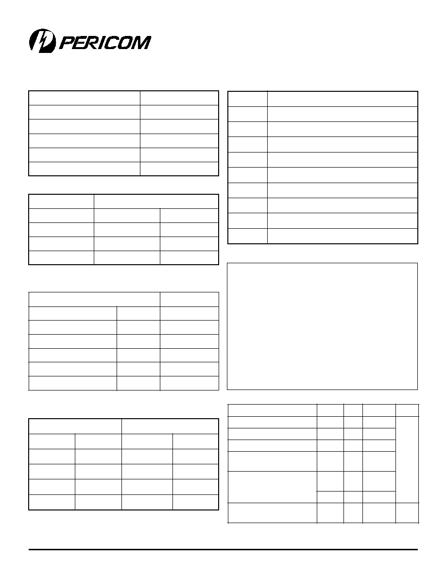
Product Features
Signaling Rates >660 Mbps (330 MHz)
Single 3.3V Power Supply Design
Driver:
±350mV Differential Swing into a 50-ohm load
Propogation Delay of 1.5ns Typ.
Low Voltage TTL (LVTTL) Inputs are 5V Tolerant
Driver is High Impedance when Disabled or V
CC
< 1.5V
Receiver:
Accepts ±50mV (min.) Differential Swing with up to 2.0V
ground potential difference
Propagation Delay of 3.3ns Typ.
Low Voltage TTL (LVTTL) Outputs
Open, Short, and Terminated Fail Safe
Industrial Temperature Operating Range: 40∞C to 85∞C
Package Options: SOIC, TSSOP, MSOP
Bus-Terminal ESD >12kV
3.3V Boost LVDS High-Speed Differential Line Drivers and Receivers
PI90LVB051
PI90LVB050
PI90LVB180
PI90LVB179
VCC
DIN1
DOUT1+
DOUT1≠
DEN
DOUT2≠
DOUT2+
DIN2
RIN1≠
RIN1+
ROUT1
REN*
ROUT2
RIN2+
RIN2≠
GND
1
2
3
4
5
6
7
8
16
15
14
13
12
11
10
9
VCC
ROUT
RIN+
RIN≠
DOUT≠
DOUT+
DIN
GND
1
2
3
4
8
7
6
5
VCC
DIN1
DOUT1+
DOUT1≠
DEN2
DOUT2≠
DOUT2+
DIN2
RIN1≠
RIN1+
ROUT1
DEN1
ROUT2
RIN2+
RIN2≠
GND
1
2
3
4
5
6
7
8
16
15
14
13
12
11
10
9
VCC
VCC
RIN+
RIN≠
DOUT≠
DOUT+
NC
NC
ROUT
REN*
DEN
DIN
GND
GND
1
2
3
4
5
6
7
14
13
12
11
10
9
8
DIN1
DEN1
DIN2
DEN2
ROUT1
ROUT2
DOUT1+
DOUT1-
DOUT2+
DOUT2-
RIN1+
RIN1-
RIN2+
RIN2-
DIN1
DIN2
DEN
ROUT2
ROUT1
REN*
DOUT1+
DOUT1-
DOUT2+
DOUT2-
RIN1+
RIN1-
RIN2+
RIN2-
DIN
DEN
ROUT
REN*
DOUT+
DOUT-
RIN+
RIN-
DIN
ROUT
DOUT+
DOUT-
RIN+
RIN-
8-Pin
U, W
16-Pin
L, W
14-Pin
L, W
16-Pin
L, W
Product Description
The PI90LVB179, PI90LVB180, PI90LVB050, and PI90LVB051 are
differential line drivers and receivers (transceivers) that are similar
to the IEEE 1596.3 SCI and ANSI/TIA/EIA-644 LVDS standards (the
difference is that the driver output current is doubled). This modi-
fication enables true half-duplex operation with more than one
LVDS driver or with two line transmission resistors over a 50-ohm
differential transmission line. These devices use low-voltage dif-
ferential signaling (LVDS) to achieve data rates in excess of 660 Mbps
while being less susceptible to noise than single-ended transmission.
The drivers translate a low-voltage TTL/CMOS input into a low-
voltage (350mV typical) differential output signal into a 50-ohm
load. The receivers translate a differential 350mV input signal to a
3V CMOS output level. Driver section can be independently set to a
power-down & high-impedance output mode with the D
EN
pin (active
HIGH). Receiver section is controlled by the R
EN*
pin (active LOW).
Applications
Applications include point-to-point and multidrop baseband data
transmission over a controlled impedance media of approximately
50 ohms. These include intra-system connections via printed circuit
board traces or cables, hubs and routers for data communications;
PBXs, switches, repeaters & base stations for telecommunications
and other applications such as digital cameras, printers and copiers.
2
PS8540A 08/07/01
12345678901234567890123456789012123456789012345678901234567890121234567890123456789012345678901212345678901234567890123456789012123456789012
12345678901234567890123456789012123456789012345678901234567890121234567890123456789012345678901212345678901234567890123456789012123456789012
PI90LVB179/PI90LVB180/
PI90LVB050/PI90LVB051
3.3V Boost LVDS High-Speed Differential Line Drivers & Receivers
Function Tables
Pin Descriptions
PI90LVB179 Receiver
t
u
p
n
I
t
u
p
t
u
O
D
N
I
D
+
T
U
O
D
T
U
O
L
L
H
H
H
L
n
e
p
o
L
H
e
m
a
N
n
o
it
p
i
r
c
s
e
D
D
N
I
s
n
i
p
t
u
p
n
i
r
e
v
ir
d
S
O
M
C
/
L
T
T
D
OUT
+
s
n
i
p
t
u
p
t
u
o
r
e
v
ir
d
g
n
it
r
e
v
n
i
-
n
o
N
D
OUT
+
s
n
i
p
t
u
p
t
u
o
r
e
v
ir
d
g
n
it
r
e
v
n
I
R
OUT
s
n
i
p
t
u
p
t
u
o
r
e
v
i
e
c
e
r
S
O
M
C
/
L
T
T
R
N
I
+
s
n
i
p
t
u
p
n
i
r
e
v
i
e
c
e
r
g
n
it
r
e
v
n
i
-
n
o
N
R
N
I
s
n
i
p
t
u
p
n
i
r
e
v
i
e
c
e
r
g
n
it
r
e
v
n
I
V
D
I
e
g
a
tl
o
V
l
a
n
g
i
S
l
ai
t
n
e
r
e
ff
i
D
t
u
p
n
I
D
N
G
n
i
p
d
n
u
o
r
G
V
C
C
%
0
1
±
V
3
.
3
+
,
n
i
p
y
l
p
p
u
s
r
e
w
o
p
e
v
it
i
s
o
P
Absolute Maximum Ratings
Supply Voltage (V
CC
) .......................................0.5V to +4.0V
Driver
Input Voltage (D
IN
) ........................... 0.3V to (Vcc + 0.3V)
Output Voltage (D
OUT+
, D
OUT-
) ...................0.3V to +3.9V
Short Circuit Duration (D
OUT+
, D
OUT-
) ............ Continuous
Enable Input Voltage (D
EN
) ................ 0.3V to (V
CC
+ 0.3V)
Receiver
Input Voltage (R
IN+
, R
IN-
) ........................... 0.3V to +3.9V)
Output Voltage (R
OUT
) ....................... 0.3V to (V
CC
+ 0.3V)
Enable Input Voltage (R
EN*
) .............. 0.3V to (V
CC
+ 0.3V)
Storage Temperature Range ..........................65∞C to +150∞C
Lead Temperature Range Soldering (4s) .......................+260∞C
Maximum Junction Temperature ...................................+150∞C
ESD Rating ..................................................................... >12kV
s
t
u
p
n
I
t
u
p
t
u
O
V
D
I
V
=
+
N
I
R
V
N
I
R
R
T
U
O
V
D
I
V
m
0
5
H
V
<
V
m
0
5
D
I
V
m
0
5
<
?
V
D
I
V
m
0
5
L
n
e
p
o
H
PI90LVB179 Driver
Notes:
H = High Level, L = Low Level, ? = Indeterminate,
Z = High-Impedance, X = Dont Care
PI90LVB180/ PI90LVB050/PI90LVB051
Receivers
s
t
u
p
n
I
t
u
p
t
u
O
V
D
I
V
=
+
N
I
R
V
N
I
R
R
*
N
E
R
T
U
O
V
D
I
V
m
0
5
L
H
V
<
V
m
0
5
D
I
V
m
0
5
<
L
?
V
D
I
V
m
0
5
L
L
n
e
p
o
L
H
X
H
Z
s
t
u
p
n
I
t
u
p
t
u
O
D
N
I
D
N
E
D
+
T
U
O
D
T
U
O
L
H
L
H
H
H
H
L
n
e
p
o
H
L
H
X
L
Z
Z
PI90LVB180/PI90LVB050/PI90LVB051
Drivers
.
n
i
M
.
p
y
T
.
x
a
M
s
ti
n
U
V
(
e
g
a
tl
o
V
y
l
p
p
u
S
C
C
)
3
3
.
3
6
.
3
V
V
,
e
g
a
tl
o
V
t
u
p
n
I
l
e
v
e
L
h
g
i
H
H
I
2
V
,
e
g
a
tl
o
V
t
u
p
n
I
l
e
v
e
L
w
o
L
L
I
8
.
0
t
u
p
n
I
l
ai
t
n
e
r
e
ff
i
D
f
o
e
d
u
ti
n
g
a
M
V
e
g
a
tl
o
V
D
I
1
.
0
6
.
0
,
e
g
a
tl
o
V
t
u
p
n
I
e
d
o
m
-
n
o
m
m
o
C
V
C
I
)
5
g
i
F
(
V
|
D
I
| 2
/
4
.
2
V
|
D
I
| 2
/
V
C
C
8
.
0
ri
A
e
e
r
F
g
n
it
a
r
e
p
O
T
e
r
u
t
a
r
e
p
m
e
T
A
0
4
5
8
C
∞
Recommended Operating Conditions
123456789012345678901234567890121234567890123456789012345678901212345678901234567890123456789012123456789012345678901234567890121234567890123
123456789012345678901234567890121234567890123456789012345678901212345678901234567890123456789012123456789012345678901234567890121234567890123
3
PS8540A 08/07/01
PI90LVB179/PI90LVB180/
PI90LVB050/PI90LVB051
3.3V Boost LVDS High-Speed Differential Line Drivers & Receivers
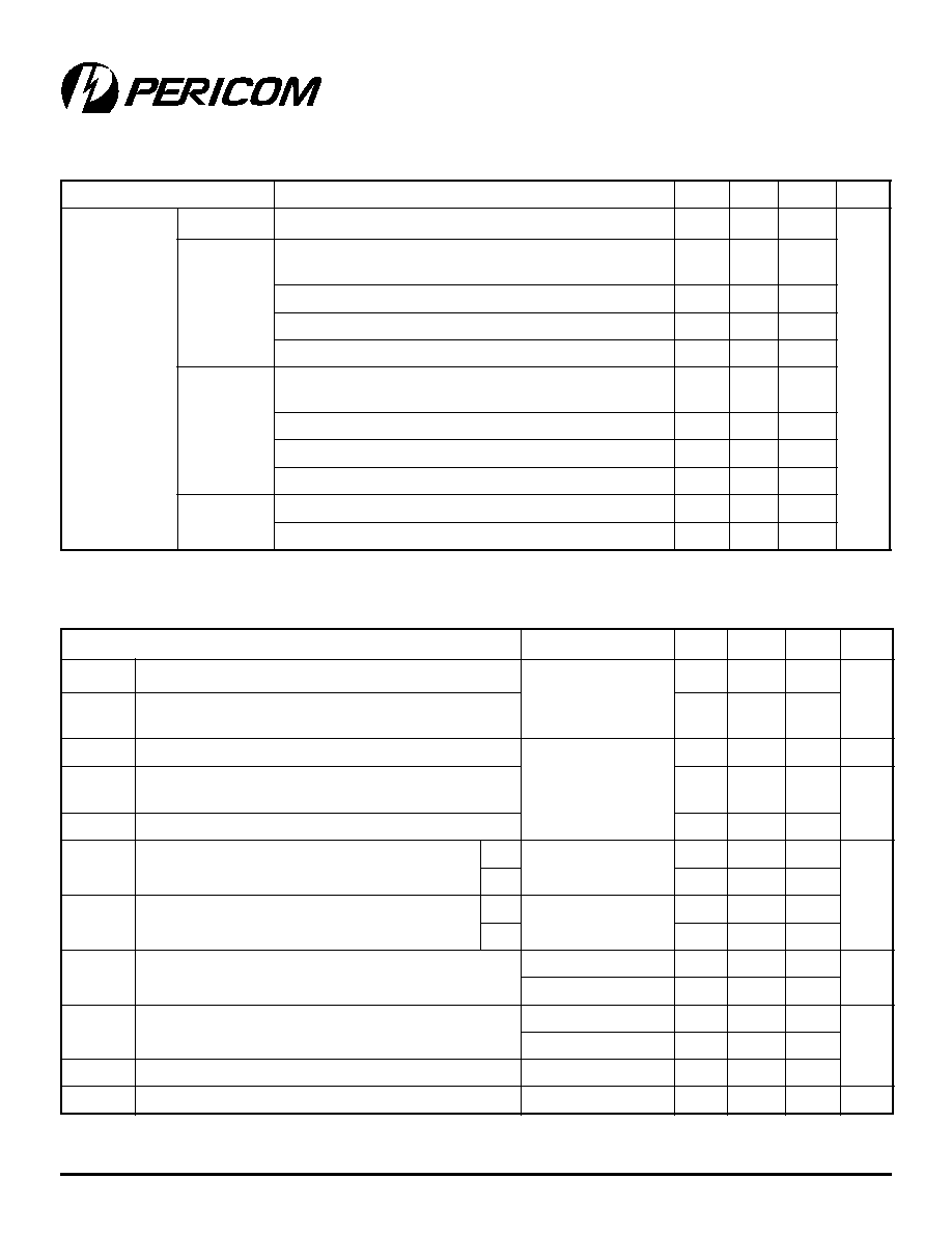
Electrical Characteristics
(Over recommended operating conditions unless otherwise noted).
r
e
t
e
m
a
r
a
P
n
o
it
i
d
n
o
C
t
s
e
T
.
n
i
M
.
p
y
T
.
x
a
M
s
ti
n
U
I
C
C
y
l
p
p
u
S
*
t
n
e
rr
u
C
9
7
1
B
V
L
0
9
I
P
R
r
e
v
ir
D
,
d
a
o
l
r
e
v
i
e
c
e
r
o
N
L
s
m
h
o
0
5
=
4
1
5
.
9
1
A
m
0
8
1
B
V
L
0
9
I
P
,
d
a
o
l
r
e
v
i
e
c
e
r
o
N
.
d
el
b
a
n
e
r
e
v
i
e
c
e
r
d
n
a
r
e
v
ir
D
R
r
e
v
ir
D
L
s
m
h
o
0
5
=
5
.
2
1
4
.
6
1
R
,
d
el
b
a
si
d
r
e
v
i
e
c
e
R
,
d
el
b
a
n
e
r
e
v
ir
D
L
s
m
h
o
0
5
=
2
.
0
1
4
1
d
a
o
l
o
N
,
d
el
b
a
n
e
r
e
v
i
e
c
e
R
,
d
el
b
a
si
d
r
e
v
ir
D
4
.
3
5
d
el
b
a
si
D
8
.
0
5
.
1
0
5
0
B
V
L
0
9
I
P
,s
d
a
o
l
r
e
v
i
e
c
e
r
o
N
.
d
el
b
a
n
e
s
r
e
v
i
e
c
e
r
d
n
a
r
e
v
ir
D
R
r
e
v
ir
D
L
s
m
h
o
0
5
=
5
2
0
3
R
,
d
el
b
a
si
d
s
r
e
v
i
e
c
e
R
,
d
el
b
a
n
e
s
r
e
v
ir
D
L
s
m
h
o
0
5
=
8
.
4
1
0
2
s
d
a
o
l
o
N
,
d
el
b
a
n
e
s
r
e
v
i
e
c
e
R
,
d
el
b
a
si
d
s
r
e
v
ir
D
6
8
d
el
b
a
si
D
8
.
0
3
.
1
1
5
0
B
V
L
0
9
I
P
R
r
e
v
ir
D
,s
d
a
o
l
r
e
v
i
e
c
e
r
o
N
,
d
el
b
a
n
e
s
r
e
v
ir
D
L
s
m
h
o
0
5
=
7
2
3
3
s
d
a
o
l
o
N
,
d
el
b
a
si
d
s
r
e
v
ir
D
5
.
6
8
.
8
All typical values are at 25∞C with a 3.3V supply
*I
CC
measured with all TTL input. V
IN
= V
CC
or GND.
Driver Electrical Characteristics
(Over recommended operating conditions unless otherwise noted).
r
e
t
e
m
a
r
a
P
s
n
o
it
i
d
n
o
C
t
s
e
T
.
n
i
M
.
p
y
T
.
x
a
M
s
ti
n
U
V
D
O
e
d
u
ti
n
g
a
m
e
g
a
tl
o
v
t
u
p
t
u
o
l
ai
t
n
e
r
e
ff
i
D
R
L
s
m
h
o
0
5
=
2
d
n
a
1
s
e
r
u
g
i
F
e
e
S
7
4
2
0
8
3
5
7
4
V
m
V
D
O
n
e
e
w
t
e
b
e
d
u
ti
n
g
a
m
e
g
a
tl
o
v
t
u
p
t
u
o
l
ai
t
n
e
r
e
ff
i
d
n
i
e
g
n
a
h
C
s
e
t
a
t
s
ci
g
o
l
0
5
0
5
V
)
S
S
(
C
O
e
g
a
tl
o
v
t
u
p
t
u
o
e
d
o
m
-
n
o
m
m
o
c
e
t
a
t
s
-
y
d
a
e
t
S
3
e
r
u
g
i
F
e
e
S
5
2
1
.
1
5
2
.
1
5
7
3
.
1
V
V
)
S
S
(
C
O
e
g
a
tl
o
v
t
u
p
t
u
o
e
d
o
m
-
n
o
m
m
o
c
e
t
a
t
s
-
y
d
a
e
t
s
n
i
e
g
n
a
h
C
s
e
t
a
t
s
ci
g
o
l
n
e
e
w
t
e
b
0
5
0
5
V
m
V
)
P
P
(
C
O
e
g
a
tl
o
v
t
u
p
t
u
o
e
d
o
m
-
n
o
m
m
o
c
k
a
e
p
-
o
t
-
k
a
e
P
0
5
0
5
1
I
H
I
t
n
e
rr
u
c
t
u
p
n
i
l
e
v
el
-
h
g
i
H
E
D
V
H
I
V
5
=
5
.
0
0
2
A
µ
D
N
I
2
0
2
I
L
I
t
n
e
rr
u
c
t
u
p
n
i
l
e
v
el
-
w
o
L
E
D
V
L
I
V
8
.
0
=
5
.
0
0
1
D
N
I
2
0
1
I
S
O
t
n
e
rr
u
c
t
u
p
t
u
o
ti
u
c
ri
c
-t
r
o
h
S
V
Y
O
V
r
o
Z
O
V
0
=
1
1
5
1
A
m
V
D
O
V
0
=
2
1
5
1
I
Z
O
t
n
e
rr
u
c
t
u
p
t
u
o
e
c
n
a
d
e
p
m
i
-
h
g
i
H
V
D
O
V
m
0
0
6
=
1
±
A
µ
V
O
V
r
o
V
0
-
C
C
1
±
I
)
F
F
O
(
O
t
n
e
rr
u
c
t
u
p
t
u
o
ff
o
-r
e
w
o
P
V
C
C
V
,
V
0
=
O
V
6
.
3
=
1
±
C
N
I
e
c
n
a
ti
c
a
p
a
c
t
u
p
n
I
7
F
p
4
PS8540A 08/07/01
12345678901234567890123456789012123456789012345678901234567890121234567890123456789012345678901212345678901234567890123456789012123456789012
12345678901234567890123456789012123456789012345678901234567890121234567890123456789012345678901212345678901234567890123456789012123456789012
PI90LVB179/PI90LVB180/
PI90LVB050/PI90LVB051
3.3V Boost LVDS High-Speed Differential Line Drivers & Receivers
r
e
t
e
m
a
r
a
P
s
n
o
it
i
d
n
o
C
t
s
e
T
.
n
i
M
.
p
y
T
.
x
a
M
s
ti
n
U
V
+
H
T
I
d
l
o
h
s
e
r
h
t
e
g
a
tl
o
v
t
u
p
n
i
l
ai
t
n
e
r
e
ff
i
d
g
n
i
o
g
-
e
v
it
i
s
o
P
1
el
b
a
T
&
5
s
e
r
u
g
i
F
e
e
S
0
5
V
m
V
H
T
I
d
l
o
h
s
e
r
h
t
e
g
a
tl
o
v
t
u
p
n
i
l
ai
t
n
e
r
e
ff
i
d
g
n
i
o
g
-
e
v
it
a
g
e
N
0
5
V
H
O
e
g
a
tl
o
v
t
u
p
t
u
o
l
e
v
el
-
h
g
i
H
I
H
O
A
m
8
=
4
.
2
V
V
L
O
e
g
a
tl
o
v
t
u
p
t
u
o
l
e
v
el
-
w
o
L
I
L
O
A
m
8
=
4
.
0
V
I
I
R
(
t
n
e
rr
u
c
t
u
p
n
I
+
N
I
R
r
o
N
I
)
V
I
0
=
2
1
1
0
2
A
µ
V
I
V
4
.
2
=
2
.
1
3
I
)
F
F
O
(
I
R
(
t
n
e
rr
u
c
t
u
p
n
i
ff
o
-r
e
w
o
P
+
N
I
R
r
o
N
I
)
V
C
C
0
=
0
2
±
I
H
)
s
el
b
a
n
e
(
t
n
e
rr
u
c
t
u
p
n
i
l
e
v
el
-
h
g
i
H
V
H
I
V
2
=
0
1
±
I
L
)
s
el
b
a
n
e
(
t
n
e
rr
u
c
t
u
p
n
i
l
e
v
el
-
w
o
L
V
L
I
V
8
.
0
=
0
1
±
I
Z
O
t
n
e
rr
u
c
t
u
p
t
u
o
e
c
n
a
d
e
p
m
i
-
h
g
i
H
V
O
V
5
r
o
0
=
0
1
±
C
I
e
c
n
a
ti
c
a
p
a
c
t
u
p
n
I
6
.
6
F
p
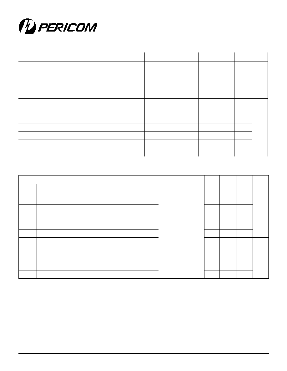
Receiver Electrical Characteristics
(Over recommended operating conditions unless otherwise noted).
Driver Switching Characteristics
(Over recommended operating conditions unless otherwise noted).
All typical values are at 25∞C with a 3.3V supply
All typical values are at 25∞C with a 3.3V supply
t
sk(o)
: the maximum delay time difference between drivers on the same device.
** t
sk(pp)
: magnitude of difference in propagation delay times between any specific terminals of two devices (all things being equal)
r
e
t
e
m
a
r
a
P
s
n
o
it
i
d
n
o
C
t
s
e
T
.
n
i
M
.
p
y
T
.
x
a
M
s
ti
n
U
t
H
L
P
t
u
p
t
u
o
l
e
v
el
-
h
g
i
h
-
o
t
-
w
o
l
,
e
m
it
y
al
e
d
n
o
it
a
g
a
p
o
r
P
R
L
s
m
h
o
0
5
=
C
L
F
p
0
1
=
2
e
r
u
g
i
F
e
e
S
7
.
1
6
.
2
s
n
t
L
H
P
t
u
p
t
u
o
l
e
v
el
-
w
o
l
-
o
t
-
h
g
i
h
l
,
e
m
it
y
al
e
d
n
o
it
a
g
a
p
o
r
P
7
.
1
6
.
2
t
r
e
m
it
e
si
r
l
a
n
g
i
s
t
u
p
t
u
o
l
ai
t
n
e
r
e
ff
i
D
4
.
0
8
.
0
t
f
e
m
it
ll
a
f
l
a
n
g
i
s
t
u
p
t
u
o
l
ai
t
n
e
r
e
ff
i
D
4
.
0
8
.
0
t
)
p
(
k
s
t(
w
e
k
s
e
sl
u
P
L
H
P
t
H
L
P
)
0
5
2
0
6
3
s
p
t
)
o
(
k
s
w
e
k
s
t
u
p
t
u
o
l
e
n
n
a
h
c
-
o
t
-l
e
n
n
a
h
C
0
9
0
6
1
t
)
p
p
(
k
s
*
*
w
e
k
s
tr
a
p
-t
r
a
p
-t
r
a
P
9
.
0
s
n
t
H
Z
P
t
u
p
t
u
o
l
e
v
el
-
h
g
i
h
-
o
t
-
e
c
n
a
d
e
p
m
i
-
h
g
i
h
,
e
m
it
y
al
e
d
n
o
it
a
g
a
p
o
r
P
7
e
r
u
g
i
F
e
e
S
3
5
t
L
Z
P
t
u
p
t
u
o
l
e
v
el
-
w
o
l
-
o
t
-
e
c
n
a
d
e
p
m
i
-
h
g
i
h
,
e
m
it
y
al
e
d
n
o
it
a
g
a
p
o
r
P
3
5
t
Z
H
P
t
u
p
t
u
o
e
c
n
a
d
e
p
m
i
-
h
g
i
h
-
o
t
-l
e
v
el
-
h
g
i
h
,
e
m
it
y
al
e
d
n
o
it
a
g
a
p
o
r
P
3
5
t
Z
L
P
t
u
p
t
u
o
e
c
n
a
d
e
p
m
i
-
h
g
i
h
-
o
t
-l
e
v
el
-
w
o
l
,
e
m
it
y
al
e
d
n
o
it
a
g
a
p
o
r
P
3
5
123456789012345678901234567890121234567890123456789012345678901212345678901234567890123456789012123456789012345678901234567890121234567890123
123456789012345678901234567890121234567890123456789012345678901212345678901234567890123456789012123456789012345678901234567890121234567890123
5
PS8540A 08/07/01
PI90LVB179/PI90LVB180/
PI90LVB050/PI90LVB051
3.3V Boost LVDS High-Speed Differential Line Drivers & Receivers
Receiving Switching Characteristics
(Over recommended operating conditions unless otherwise noted).
All typical values are at 25∞C with a 3.3V supply.
** t
sk(pp)
is magnitude of difference in propagation delay times between any specific terminals of two devices (all things being equal).
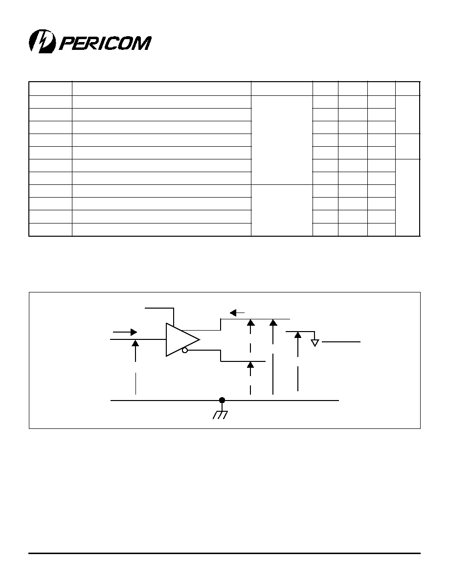
Parameter Measurement Information
DIN
VOD
II
DOD+
VOC
VOD+
VOD+VOD+
2
VOD≠
VI
DOUT+
DOUT≠
Driver
DEN
Figure 1. Driver Voltage and Current Definitions
r
e
t
e
m
a
r
a
P
s
n
o
it
i
d
n
o
C
t
s
e
T
.
n
i
M
.
p
y
T
.
x
a
M
s
ti
n
U
t
H
L
P
t
u
p
t
u
o
l
e
v
el
-
h
g
i
h
-
o
t
-
w
o
l
,
e
m
it
y
al
e
d
n
o
it
a
g
a
p
o
r
P
C
L
F
p
0
1
=
6
e
r
u
g
i
F
e
e
S
2
0
.
3
s
n
t
L
H
P
t
u
p
t
u
o
l
e
v
el
-
w
o
l
-
o
t
-
h
g
i
h
l
,
e
m
it
y
al
e
d
n
o
it
a
g
a
p
o
r
P
1
.
2
0
.
3
t
*
*
)
p
p
(
k
s
*
*
w
e
k
s
tr
a
p
-t
r
a
p
-t
r
a
P
0
.
1
t
)
p
(
k
s
t(
w
e
k
s
e
sl
u
P
L
H
P
t
H
L
P
)
0
0
3
0
5
7
s
p
t
)
o
(
k
s
w
e
k
s
l
e
n
n
a
h
c
-
o
t
-l
e
n
n
a
h
C
0
6
t
r
e
m
it
e
si
r
l
a
n
g
i
s
t
u
p
t
u
O
0
.
1
5
.
1
s
n
t
f
e
m
it
ll
a
f
l
a
n
g
i
s
t
u
p
t
u
O
2
.
1
8
.
1
t
H
Z
P
t
u
p
t
u
o
e
c
n
a
d
e
p
m
i
-
h
g
i
h
-
o
t
-l
e
v
el
-
h
g
i
h
,
e
m
it
y
al
e
d
n
o
it
a
g
a
p
o
r
P
7
e
r
u
g
i
F
e
e
S
7
.
1
3
.
2
t
L
Z
P
t
u
p
t
u
o
e
c
n
a
d
e
p
m
i
-
w
o
l
-
o
t
-l
e
v
el
-
w
o
l
,
e
m
it
y
al
e
d
n
o
it
a
g
a
p
o
r
P
5
.
4
7
.
5
t
Z
H
P
t
u
p
t
u
o
l
e
v
el
-
h
g
i
h
-
o
t
-
e
c
n
a
d
e
p
m
i
-
h
g
i
h
,
e
m
it
y
al
e
d
n
o
it
a
g
a
p
o
r
P
5
.
2
2
.
3
t
Z
L
P
t
u
p
t
u
o
l
e
v
el
-
h
g
i
h
-
o
t
-
e
c
n
a
d
e
p
m
i
-
w
o
l
,
e
m
it
y
al
e
d
n
o
it
a
g
a
p
o
r
P
0
.
6
8
.
7
6
PS8540A 08/07/01
12345678901234567890123456789012123456789012345678901234567890121234567890123456789012345678901212345678901234567890123456789012123456789012
12345678901234567890123456789012123456789012345678901234567890121234567890123456789012345678901212345678901234567890123456789012123456789012
PI90LVB179/PI90LVB180/
PI90LVB050/PI90LVB051
3.3V Boost LVDS High-Speed Differential Line Drivers & Receivers
Driver (continued)
2 V
1.4 V
0.8 V
100%
80%
20%
0%
0 V
VOD(H)
VOD(L)
Output
VOD
50
±1%
CL = 10 pF
(2 Places)
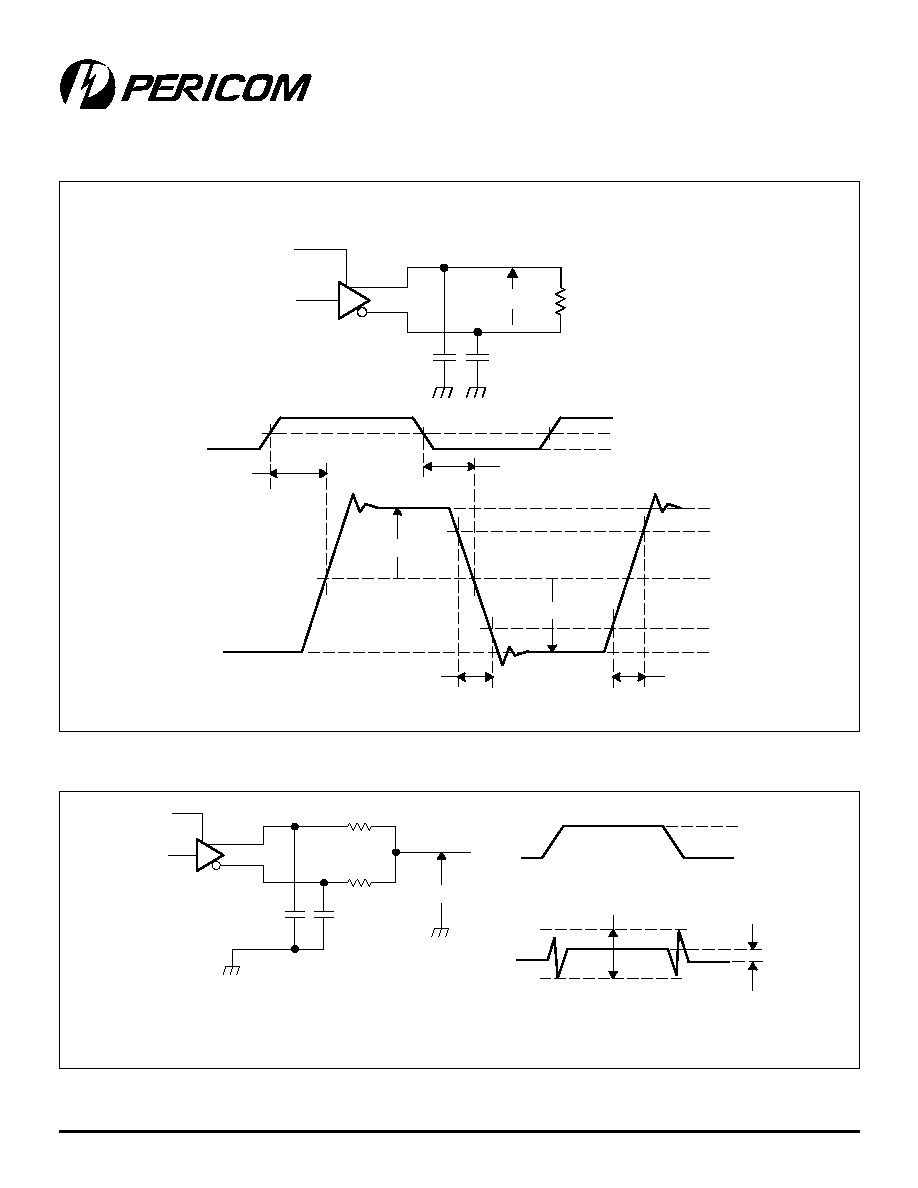
tPHL
tPLH
tf
tr
D
EN
D
OUT+
D
OUT≠
D
IN
D
IN
D
EN
D
OUT+
D
OUT≠
D
IN
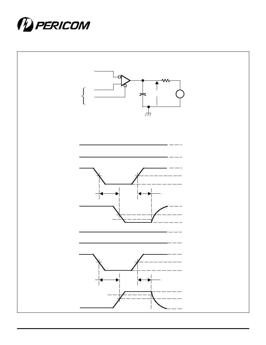
NOTE A: All input pulses are supplied by a generator having the following characteristics: tr or tf
1 ns, pulse repetition rate (PRR) = 50 Mpps,
pulse width = 10
±
0.2 ns . CL includes instrumentation and fixture capacitance within 0.06 mm of the D.U.T.
VOC
CL = 10 pF
(2 Places)
3 V
0 V
VOC(PP)
VOC(SS)
VOC
25
,
±
1% (2 Places)
NOTE A: All input pulses are supplied by a generator having the following characteristics: tr or tf
1 ns, pulse repetition rate (PRR) = 50 Mpps,
pulse width = 10
±
0.2 ns . CL includes instrumentation and fixture capacitance within 0.06 mm of the D.U.T. The measurement of VOC(PP)
is made on test equipment with a ≠3 dB bandwidth of at least 300 MHz.
Parameter Measurement Information
Figure 2. Test Circuit, Timing, and Voltage Definitions for the Differential Output Signal
Figure 3. Test Circuit and Definitions for the Driver Common-Mode Output Voltage
123456789012345678901234567890121234567890123456789012345678901212345678901234567890123456789012123456789012345678901234567890121234567890123
123456789012345678901234567890121234567890123456789012345678901212345678901234567890123456789012123456789012345678901234567890121234567890123
7
PS8540A 08/07/01
PI90LVB179/PI90LVB180/
PI90LVB050/PI90LVB051
3.3V Boost LVDS High-Speed Differential Line Drivers & Receivers
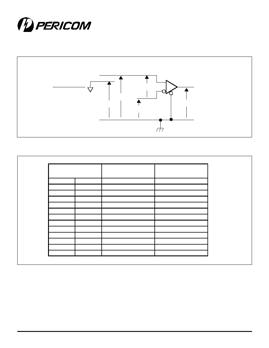
Driver (continued)
1.2 V
25
±1% (2 Places)
C
L
=10pF
(2 Places)
2 V
0.8 V
tPHZ
tPZH
tPLZ
tPZL
1.4 V
~1.4 V
1.2 V
1.25 V
1.2 V
~1 V
1.15 V
at 0.8 V and input to D
EN
NOTE A: All input pulses are supplied by a generator having the following characteristics: tr or tf
1 ns, pulse repetition rate (PRR) = 0.5 Mpps,
pulse width = 500
±
10 ns . CL includes instrumentation and fixture capacitance within 0.06 mm of the D.U.T.
D
IN at
0.8V or 2V
D
EN
D
OUT+
V
OD+
V
OD+
or V
OD≠
V
OD≠
or V
OD+
V
OD≠
D
OUT≠
D
EN
D
IN
at 2V and input to
D
EN
D
IN
Parameter Measurement Information (continued)
Figure 4. Enable and Disable Timing Circuit and Definitions
8
PS8540A 08/07/01
12345678901234567890123456789012123456789012345678901234567890121234567890123456789012345678901212345678901234567890123456789012123456789012
12345678901234567890123456789012123456789012345678901234567890121234567890123456789012345678901212345678901234567890123456789012123456789012
PI90LVB179/PI90LVB180/
PI90LVB050/PI90LVB051
3.3V Boost LVDS High-Speed Differential Line Drivers & Receivers
Receiver
V
ID
V
IC
V
O
R
IN+
R
IN≠
V
IRIN+
V
IRIN+
R
OUT
V
IRIN
++V
IRIN≠
V
IRIN≠
V
IRIN+
2
APPLIED VOLTAGES
(V)
RESULTING DIFFERENTIAL
INPUT VOLTAGE
(mV)
RESULTING COMMON-
MODE INPUT VOLTAGE
(V)
V
ID
V
IC
1.225
1.175
50
1.2
1.175
1.225
1.2
2.375
2.325
50
2.35
2.325
2.375
2.35
0.1
0
50
0.05
0
0.05
≠50
0.05
≠50
≠50
1.5
0.9
600
1.2
0.9
1.5
1.2
2.4
1.8
600
2.1
1.8
2.4
2.1
0.6
0
600
0.3
0
0.6
≠600
≠600
≠600
0.3
Parameter Measurement Information (continued)
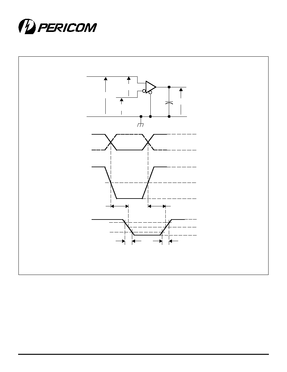
Figure 5. Receiver Voltage Definitions
Table 1. Receiver Minimum and Maximum Input Threshold Test Voltages
123456789012345678901234567890121234567890123456789012345678901212345678901234567890123456789012123456789012345678901234567890121234567890123
123456789012345678901234567890121234567890123456789012345678901212345678901234567890123456789012123456789012345678901234567890121234567890123
9
PS8540A 08/07/01
PI90LVB179/PI90LVB180/
PI90LVB050/PI90LVB051
3.3V Boost LVDS High-Speed Differential Line Drivers & Receivers
Receiver (continued)
V
ID
V
IRIN+
V
IRIN+
V
IRIN≠
V
IRIN≠
V
O
C
L
10pF
V
OH
V
OL
1.4 V
V
O
V
ID
1.4 V
1 V
0.4 V
0 V
≠ 0.4 V
t
PHL
t
PLH
tr
tf
0.4 V
2.4 V
NOTE A: All input pulses are supplied by a generator having the following characteristics: tr or tf
1 ns, pulse repetition rate (PRR) = 50 Mpps,
pulse width = 10
±
0.2 ns. CL includes instrumentation and fixture capacitance within 0.06 m of the D.U.T.
Parameter Measurement Information (continued)
Figure 6. Timing Test Circuit and Waveforms
10
PS8540A 08/07/01
12345678901234567890123456789012123456789012345678901234567890121234567890123456789012345678901212345678901234567890123456789012123456789012
12345678901234567890123456789012123456789012345678901234567890121234567890123456789012345678901212345678901234567890123456789012123456789012
PI90LVB179/PI90LVB180/
PI90LVB050/PI90LVB051
3.3V Boost LVDS High-Speed Differential Line Drivers & Receivers
Receiver (continued)
V
O
C
L
10 pF
+
≠
500
1.2 V
R
IN≠
R
IN+
R
EN*
R
EN*
R
EN*
R
OUT
R
OUT
Inputs
V
TEST
NOTE A: All input pulses are supplied by a genertor having the following characteristics: tr or tf
1ns,
pulse repetition rate (PRR) = 0.5 Mpps, pulse wide = 500 ±10ns. CL includes instrumentation
and fixture capacitance within 0.06m of the D.U.T.
t
PZL
V
TEST
t
PZL
t
PLZ
2.5 V
1.4 V
V
OL
+0.5 V
V
OL
2 V
1.4 V
0.8 V
2.5 V
1 V
t
PZH
R
IN+
V
TEST
t
PZH
t
PHZ
V
OH
1.4 V
V
OH
≠0.5 V
0 V
2 V
1.4 V
0.8 V
0 V
1.4 V
R
IN*
Parameter Measurement Information (continued)
Figure 7. Enable/Disable Time Test Circuit and Waveforms

123456789012345678901234567890121234567890123456789012345678901212345678901234567890123456789012123456789012345678901234567890121234567890123
123456789012345678901234567890121234567890123456789012345678901212345678901234567890123456789012123456789012345678901234567890121234567890123
11
PS8540A 08/07/01
PI90LVB179/PI90LVB180/
PI90LVB050/PI90LVB051
3.3V Boost LVDS High-Speed Differential Line Drivers & Receivers
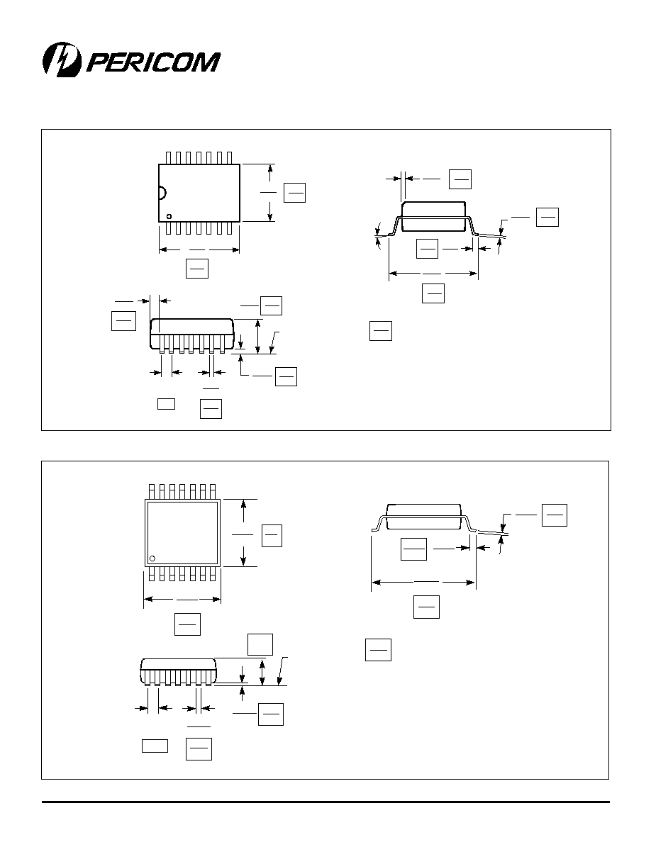
8-Pin SOIC W Package
8-Pin Mini Small Outline U Package (MSOP)
.0040
.0098
SEATING PLANE
.013
.020
.050
BSC
.016
.0075
.0098
1
8
.0099
.0196
0-8∞
.050
.149
.157
X.XX
X.XX
DENOTES DIMENSIONS
IN MILLIMETERS
3.78
3.99
.189
.196
4.80
5.00
1.27
.016
.026
1.35
1.75
.2284
.2440
5.80
6.20
0.406
0.660
0.330
0.508
0.10
0.25
0.40
1.27
0.19
0.25
0.25
0.50
x 45∞
.053
.068
REF
12
PS8540A 08/07/01
12345678901234567890123456789012123456789012345678901234567890121234567890123456789012345678901212345678901234567890123456789012123456789012
12345678901234567890123456789012123456789012345678901234567890121234567890123456789012345678901212345678901234567890123456789012123456789012
PI90LVB179/PI90LVB180/
PI90LVB050/PI90LVB051
3.3V Boost LVDS High-Speed Differential Line Drivers & Receivers
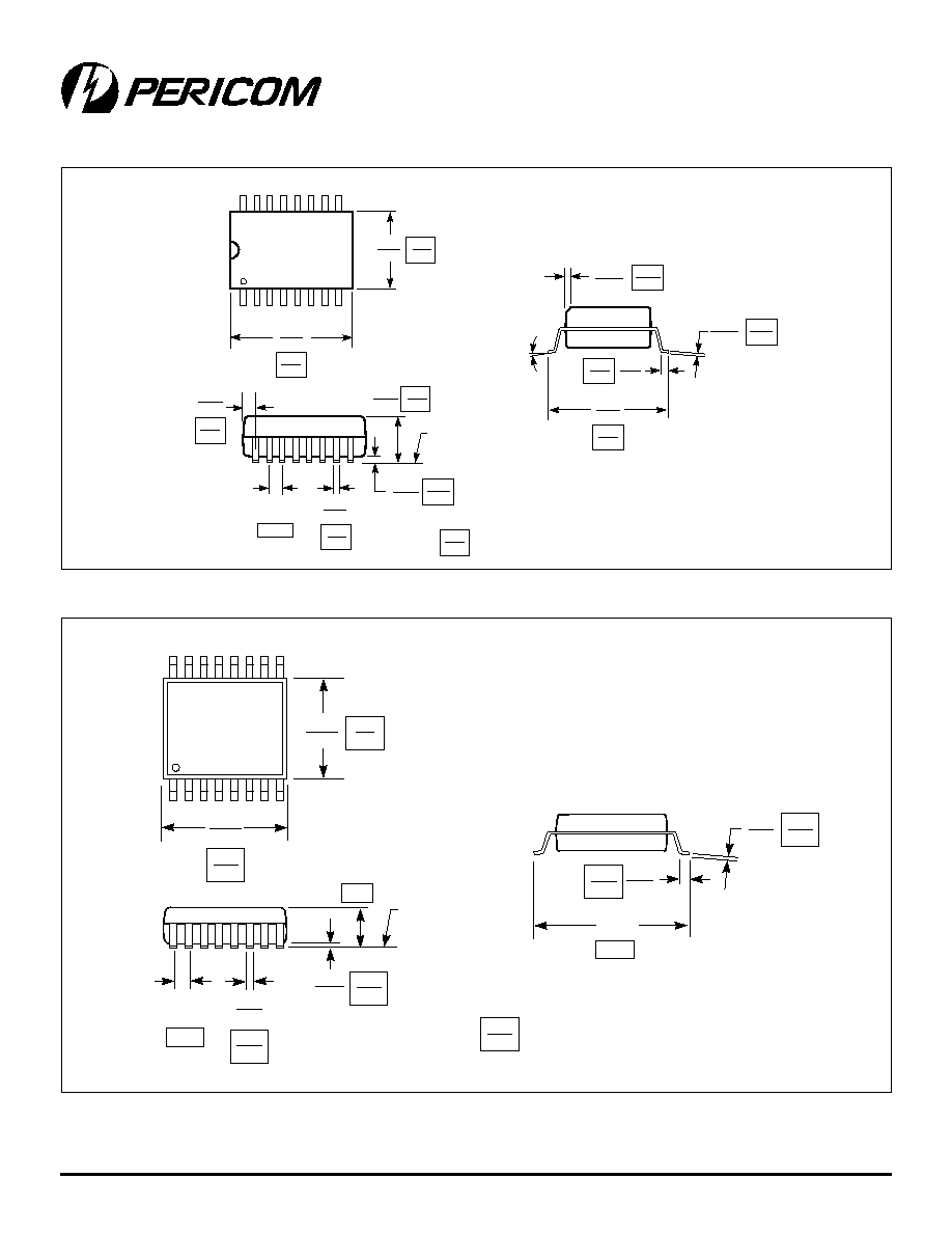
14-Pin TSSOP (4.4mm wide) L Package
14-Pin SOIC (150 Mil) W Package
SEATING PLANE
.050
BSC
1
14
x 45∞
0-8∞
.149
.157
X.XX
X.XX
DENOTES DIMENSIONS
IN MILLIMETERS
3.78
3.99
.336
.344
8.55
8.75
.0155
.026
0.393
0.660
1.27
.053
.068
1.35
1.75
.2284
.2440
5.80
6.20
.013
.020
0.330
0.508
.0040
.0098
0.10
0.25
.0099
.0196
0.25
0.50
.0075
.0098
0.19
0.25
.016
.050
0.41
1.27
REF
0.193
0.201
0.047
0.002
0.006
SEATING
PLANE
0.0256
typical
0.018
0.030
0.004
0.008
0.240
0.264
1
14
0.169
0.177
X.XX
X.XX
DENOTES DIMENSIONS
IN MILLIMETERS
0.05
0.15
6.1
6.7
0.45
0.75
0.09
0.20
4.3
4.5
1.20
max.
4.90
5.10
0.65
0.19
0.30
0.007
0.012
123456789012345678901234567890121234567890123456789012345678901212345678901234567890123456789012123456789012345678901234567890121234567890123
123456789012345678901234567890121234567890123456789012345678901212345678901234567890123456789012123456789012345678901234567890121234567890123
13
PS8540A 08/07/01
PI90LVB179/PI90LVB180/
PI90LVB050/PI90LVB051
3.3V Boost LVDS High-Speed Differential Line Drivers & Receivers
16-Pin SOIC (150 Mil) W Package
16-Pin TSSOP (4.4mm wide) L Package
SEATING PLANE
.050
BSC
1
16
0-8∞
.149
.157
X.XX
X.XX
DENOTES DIMENSIONS
IN MILLIMETERS
3.78
3.99
.386
.393
9.80
10.00
1.27
.053
.068
1.35
1.75
.2284
.2440
5.80
6.20
.0040
.0098
0.10
0.25
.013
.020
.0155
.0260
0.330
0.508
0.393
0.660
.0075
.0098
0.25
0.50
.0099
.0196
x 45∞
0.19
0.25
.016
.050
0.41
1.27
REF
.193
.201
.047
max.
.002
.006
SEATING
PLANE
.0256
BSC
.018
.030
.004
.008
.252
BSC
1
16
.169
.177
X.XX
X.XX
DENOTES CONTROLLING
DIMENSIONS IN MILLIMETERS
0.05
0.15
6.4
0.45
0.75
0.09
0.20
4.3
4.5
1.20
4.9
5.1
0.65
0.19
0.30
.007
.012

14
PS8540A 08/07/01
12345678901234567890123456789012123456789012345678901234567890121234567890123456789012345678901212345678901234567890123456789012123456789012
12345678901234567890123456789012123456789012345678901234567890121234567890123456789012345678901212345678901234567890123456789012123456789012
PI90LVB179/PI90LVB180/
PI90LVB050/PI90LVB051
3.3V Boost LVDS High-Speed Differential Line Drivers & Receivers
Pericom Semiconductor Corporation
2380 Bering Drive ∑ San Jose, CA 95131 ∑ 1-800-435-2336 ∑ Fax (408) 435-1100 ∑ http://www.pericom.com
t
r
a
P
e
g
a
k
c
a
P
-
n
i
P
e
r
u
t
a
r
e
p
m
e
T
W
9
7
1
B
V
L
0
9
I
P
C
I
O
S
-
8
C
∞
5
8
+
o
t
C
∞
0
4
W
0
8
1
B
V
L
0
9
I
P
C
I
O
S
-
4
1
C
∞
5
8
+
o
t
C
∞
0
4
W
0
5
0
B
V
L
0
9
I
P
C
I
O
S
-
6
1
C
∞
5
8
+
o
t
C
∞
0
4
W
1
5
0
B
V
L
0
9
I
P
C
I
O
S
-
6
1
C
∞
5
8
+
o
t
C
∞
0
4
U
9
7
1
B
V
L
0
9
I
P
P
O
S
M
-
8
C
∞
5
8
+
o
t
C
∞
0
4
L
0
8
1
B
V
L
0
9
I
P
P
O
S
S
T
-
4
1
C
∞
5
8
+
o
t
C
∞
0
4
L
0
5
0
B
V
L
0
9
I
P
P
O
S
S
T
-
6
1
C
∞
5
8
+
o
t
C
∞
0
4
L
1
5
0
B
V
L
0
9
I
P
P
O
S
S
T
-
6
1
C
∞
5
8
+
o
t
C
∞
0
4
Ordering Information