
1
PS8573C 09/22/04
2DO4 ≠
GND
1
VCC
1DIN2
1DIN3
1DIN4
EN2
2DIN4
GND
VCC
VCC
2
VCC
3
GND
4
EN1
5
1DIN1
6
7
8
9
10
2DIN1
11
2DIN2
12
2DIN3
13
14
15
16
17
GND
18
3DIN1
19
3DIN2
20
3DIN3
21
3DIN4
22
EN3
23
4DIN1
24
64
63
62
61
60
59
58
57
56
55
2DO2+
54
2DO2≠
53
2DO3+
52
51
50
49
48
47
46
45
3DO4 ≠
3DO4+
44
3DO3 ≠
3DO3+
3DO2 ≠
3DO2+
3DO1 ≠
3DO1+
2DO3 ≠
2DO4+
2DO1+
2DO1 ≠
1DO4+
1DO4 ≠
1DO3+
1DO3 ≠
1DO2+
1DO2 ≠
1DO1+
1DO1 ≠
43
42
41
25
26
27
28
29
30
31
32
40
39
37
37
36
35
34
33
4DIN4
EN3
GND
VCC
4DIN2
4DIN3
VCC
GND
4DO1 ≠
4DO4 ≠
4DO4+
4DO3 ≠
4DO3+
4DO2 ≠
4DO2+
4DO1+
Features
∑ Sixteen line drivers meet or exceed the requirements of the
ANSI EIA/TIA-644 Standard
∑ Designed for signaling rates
up to 500 Mbps with very low
radiation (EMI)
∑ Low voltage differential signaling with typical output voltage
of 350mV into :
≠ 100 load (PI90LV387)
≠ 50 load (PI90LVB387)
∑ Propagation delay times less than 2.6ns
∑ Output skew is less than 150ps
∑ Part-to-part skew is less than 1.5ns
∑ 35mW total power dissipation in each driver operating at 200
MHz
∑ Bus-pin ESD protection exceeds 10kV
∑ Low voltage TTL (LVTTL) logic inputs are 5V tolerant
∑ Packaging (Pb-free & Green available):
-64-Pin TSSOP (A)
Description
PI90LV387/ PI90LVB387 consists of sixteen differential line
drivers that implement the electrical characteristics of low-volt-
age differential signaling (LVDS). This signaling technique lowers
output voltage levels to reduce power, increase switching speeds,
and allow operation with a 3V supply rail.
The intended application of this device and signaling technique
is for point-to-point baseband (single termination) and multi-
point (double termination) data transmission over a controlled
impedance media of approximately 100 and 50 (LVB387).
The transmission media may be printed-circuit board traces, back-
planes, or cables. The large number of drivers integrated into the
same substrate, with the low pulse skew of balanced signaling,
allows extremely precise timing alignment of clock and data for
synchronous parallel data transfers. When used with its companion
16-channel receivers, the PI90LV386 or PI90LVT386, over 400
million data transfers per second in single-edge clocked systems
are possible with very little power.
(Note: The ultimate rate and distance of data transfer is dependent
upon attenuation characteristics of the media, the noise coupling
to the environment, and other system characteristics.)
The drivers are enabled in groups of five. When disabled, driver
outputs are at a high impedance. Each driver input (D
IN
) and en-
able (EN) have an internal pulldown that drives the input to a low
level when open circuited.
The parts are characterized for operation from ≠40∞C to 85∞C.
PI90LV387/ PI90LVB387
High-Speed Differential Line Drivers
D
O1+
D
IN1
D
O1≠
D
O2+
D
O2≠
D
IN2
EN
D
O3+
D
IN3
D
O3≠
D
O4+
D
O4≠
D
IN4
1 of 4
Block Diagram
Pin Diagram
64-Pin
A

2
PS8573C 09/22/04
PI90LV387/PI90LVB387
High-Speed Differential Line Drivers
Supply Voltage Range, V
CC
(2)........................................
≠0.5V to 4V
Voltage Range: Inputs ............................................ ≠0.5V to 6V
D
O+
or D
O≠
............................................................. ≠0.5V to 4V
Electrostatic Discharge
(3):
(D
O+
,D
O≠
and GND).......................Class 3, A: 10kV, B:700V
(All Pins) ..........................................Class 3, A: 8kV, B:600V
Continuous Power Dissipation......(see dissipation rating table)
Storage Temperature Range ............................. ≠65∞C to 150∞C
Lead Temperature 1.6mm (1/16 inch)
from case for 10 seconds...............................................260∞C
Absolute Maximum Ratings
(Over Operating Free-Air Temperature, unless otherwise noted)
(1)
Notes:
1. Stresses beyond those listed under "Absolute Maximum Ratings"
may cause permanent damage to the device. These are stress ratings
only, and functional operation of the device at these or any other
conditions beyond those indicated under "Recommended Operating
Conditions" is not implied. Exposure to Absolute-Maximum-Rated
conditions for extended periods may affect device reliability.
2. All voltage values, except differential I/O bus voltages, are with
respect to ground terminal.
3. Tested in accordance with MIL-STD-883C Method 3015.7
Recommended Operating Conditions
Min. Nom. Max. Units
Supply Voltage, V
CC
3.0
3.3
3.6
V
High-level Input Voltage, V
IH
2.0
Low-level Input Voltage, V
IL
0.8
Operating free-air tempera-
ture, T
A
-40
85
∫C
Driver Function Table
Differential Input
Enables
Outputs
D
IN
EN
D
OUT+
D
OUT-
H
H
H
L
L
H
L
H
X
L
Z
Z
Open
H
L
H
Notes:
1. H = high level,
L = low level,
X = irrelevent,
Z = high impedance (off)

3
PS8573C 09/22/04
PI90LV387/PI90LVB387
High-Speed Differential Line Drivers
Electrical Characteristics Over Recommended Operating Conditions
(unless otherwise noted)
Symbol
Parameter
Test Conditions
Min. Typ.
Max.
Units
| V
OH
|
Differential output voltage magnitude
R
L
= 50 (LVB)
R
L
= 100 (LV)
See Figure 1 and 2
247
340
454
mV
| V
OH
|
Change in differential output voltage
magnitude between logic states
-50
50
V
OC(SS)
Steady-state common-mode output
voltage
See Figure 3
LV
1.125
1.375
V
LVB
1.000
1.375
V
OC(SS)
Change in Steady-state common-mode
output voltage between logic states
See Figure 3
-50
50
mV
V
OC(PP)
Peak-to-peak common-mode output
voltage
50
150
I
CC
Supply Current
R
L
= 50 (LVB)
R
L
= 100 (LV)
Enabled, V
IN
= GND or V
CC
LV
60
78
mA
LVB
122
190
I
IH
High-Level input current
V
IH
= 2V
3
20
µA
I
IL
Low-level input current
V
IL
= 0.8V
2
10
I
OS
Short-circuit output current
V
ODOUT+
or V
ODOUT-
= 0V
LV
±24
mA
LVB
±48
V
OD
= 0V
LV
±12
LVB
±24
I
OZ
High-impedance output current
V
O
= 0V or V
CC
±1
µA
I
O(OFF)
Power-off output current
V
CC
= 0V, V
O
= 2.4V
±1
C
IN
Input capacitance
V
I
= 0.4 sin (4E6t) + 0.5V
6
pF
C
O
Output capacitance
V
I
= 0.4 sin (4E6t) + 0.5V,
Disabled
9.4
Note:
1. All typical values are at 25∞C and with a 3.3V supply.

4
PS8573C 09/22/04
PI90LV387/PI90LVB387
High-Speed Differential Line Drivers
Switching Characteristics
(Over Recommended Operating Conditions, unless otherwise noted)
Symbol
Parameter
Test Conditions
Min.
Typ.
Max. Units
t
PHL
Propagation delay time low-to-high level outputs
R
L
= 50 (LVB)
R
L
= 100 (LV)
C
L
= 10pF
See Figure 4
0.9
1.8
2.6
ns
t
PHL
Propagation delay time, high-to-low-level outputs
0.9
1.8
2.6
t
r
Differential outpu sign rise time
0.4
0.8
1.3
t
f
Differential output signal fall time
0.4
0.8
1.3
t
sk(p)
Pulse skew ( | tphl - tphl | )
150
500
ps
t
sk(o)
Output skew
(2)
80
150
t
sk(pp)
Part-to-part skew
(3)
1.5
t
PZH
Propagation delay time, high impdeance-to high-level output
See Figure 5
4.5
6.7
ns
t
PZL
Propagation delay time, high impdeance-to low-level output
3.5
5.1
t
PHZ
Propagation delay time, high-level-to-high-impdeance output
3.1
4.6
t
PLZ
Propagation delay time, low-level-to-high-impdeance output
3.1
4.6
f
MAX
Maximum operating frequency
250
MHz
Notes:
1. All typical values are at 25∞C and with a 3.3V supply
2. t
sk(o)
is the magnitude of the time difference between the t
PLH
or t
PHL
of all drivers of a single device with all of their inputs connected to-
gether.
3. t
sk(pp)
is the magnitude of the difference in propagation delay times between any specified terminals of two devices when both devices operate
with the same supply voltages, at the same temperature, and have identical packages and test circuits

5
PS8573C 09/22/04
PI90LV387/PI90LVB387
High-Speed Differential Line Drivers
Figure 1. Voltage and Current Definitions
Parameter Measurement Information
Figure 2. V
OD
Test Circuit
Note:
1. All input pulses are supplied by a generator having the following characteristics: t
r
or t
f
1ns, Pulse Repetition Rate
(PRR) = 50 Mpps, Pulse width = 10 ±0.2ns. C
L
includes instrumentation and fixture capacitance within 0.06m of the D.U.T. The measurement
of VOC(PP) is made on test equipment with a ≠3dB bandwidth of at least 300MHz.
Figure 3. Test Circuit & Definitions for the Driver Common-Mode Output Voltage

6
PS8573C 09/22/04
PI90LV387/PI90LVB387
High-Speed Differential Line Drivers
Note:
1. All input pulses are supplied by a generator having the following characteristics: t
r
or t
f
1ns, Pulse Repetition Rate (PRR) = 15 Mpps, Pulse
width = 10 ±0.2ns. C
L
includes instrumentation and fixture capacitance within 0.06m of the D.U.T.
Figure 4. Test Circuit, Timing, & Voltage Definitions for the Differential Output Signal
Parameter Measurement Information (continued)
Note:
1. All input pulses are supplied by a generator having the following characteristics: t
r
or t
f
1ns, Pulse Repetition Rate
(PRR) = 0.5 Mpps, Pulse width = 500 ±10ns. C
L
includes instrumentation and fixture capacitance within 0.06m of the D.U.T.
Figure 5. Enable & Disable Time Circuit & Definitions
7
PS8573C 09/22/04
PI90LV387/PI90LVB387
High-Speed Differential Line Drivers
Ordering Information
Ordering Code
Package Code
Package Type
PI90LV387A
A
64-pin TSSOP
PI90LV387AE
A
Pb-free & Green, 64-pin TSSOP
PI90LVB387A
A
64-pin TSSOP
PI90LVB387AE
A
Pb-free & Green, 64-pin TSSOP
Notes:
1. Thermal characteristics can be found on the company web site at www.pericom.com/packaging/
2. Number of Transistors = TBD
Pericom Semiconductor Corporation ∑ 1-800-435-2336 ∑ www.pericom.com
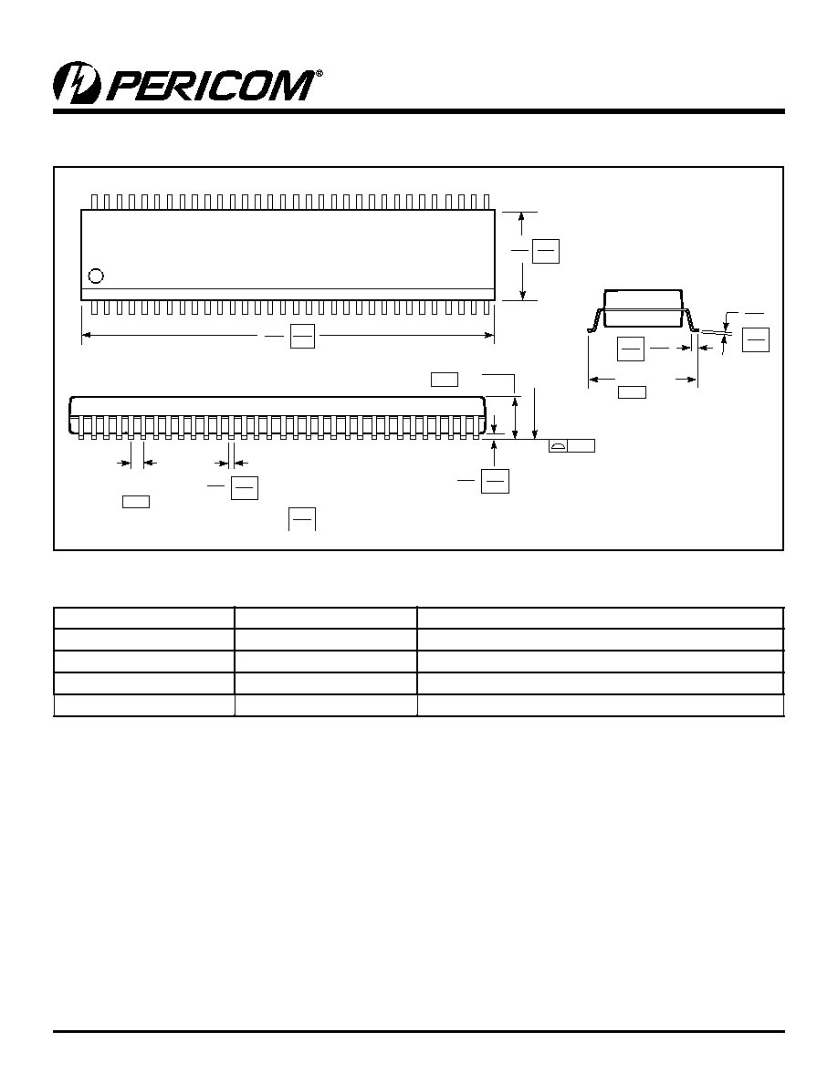
Packaging Mechanical: 64-Pin TSSOP (A)
.002
.006
SEATING
PLANE
.007
.011
.004
.008
1
64
.236
.244
0.50
0.17
0.27
0.05
0.15
0.09
0.20
X.XX
X.XX
DENOTES DIMENSIONS
IN MILLIMETERS
.018
.030
0.45
0.75
.047
Max.
1.20
6.0
6.2
.665
.673
16.9
17.1
.319
8.1
.0197
BSC
BSC
.004
0.10