
1
PS8664 02/21/03
Features
∑ Ten line receivers meet or exceed the requirements of the
ANSI TIA/EIA-644-1995 Standard
∑ Designed for signaling rates up to 660 Mbps
∑ 0V to 3V common-mode input voltage range
∑ Operates from a single 3.3V supply
∑ Typical propagation delay time: 2.6ns
∑ Output skew 100ps (typical)
∑ Part-to-part skew is less than 1ns
∑ PI90LVR3810
Set up time: typical 1ns
Max. clock to output: 1ns
∑ Integrated 110-ohm termination on PI90LVT386
∑ Low Voltage TTL (LVTTL) levels are 5V tolerant
∑ Open-circuit fail safe
∑ Flow-through pin out
∑ Packaging:
48-Pin Thin Shrink Small Output TSSOP (A)
Description
The PI90LVx3810 family consists of ten differential line receivers
with 3-state outputs that implement Low-Voltage Differential Sig-
naling (LVDS). The PI90LVR3810 has integrated edge-triggered
D-type flops. Any of the differential receivers will provide a valid
logical output state with a ±100mV differential input voltage within
the input common-mode voltage range that allows 0 to 3V of ground
potential difference between two LVDS nodes. The independent EN
pins can be used to place the outputs in either a normal logic state
(high or low logic levels) or a high-impedance state. In high-
impedance state, outputs neither load nor drive the bus lines.
The intended application of these devices, and their signaling
techniques, is for point-to-point baseband data transmission over
controlled impedance media of approximately 100-Ohms with a 100-
Ohm termination resistor. The transmission media may be printed
circuit board traces, backplanes, or cables. The PI90LV3810's 10
receivers integrated into the same substrate allow precise timing
alignment. In addition, the PI90LVR3810's integrated registers
resynchronize the data to the system clock, for additional signal
deskew.
The integrated registers in the PI90LVR3810 are particularly suitable
for interfacing with LVDS drivers such as the PI90LV3811 over long
distances where signal-to-signal skew may be a problem. On the
positive transition of the differential clock (CLK±) input, the Q
outputs of the flip-flop take on the logic levels set up at the
differential data (RIN±) inputs.
Old data can be retained or new data can be entered while the
outputs are in the high-impedance state. The EN pins do not affect
the internal operation of the flip-flops.
12345678901234567890123456789012123456789012345678901234567890121234567890123456789012345678901212345678901234567890123456789012123456789012
12345678901234567890123456789012123456789012345678901234567890121234567890123456789012345678901212345678901234567890123456789012123456789012
PI90LV3810/PI90LVR3810
High-Speed Differential
Line Receivers
PI90LV3810
PI90LVR3810 Truth Table
T
E
S
R
T
U
O
0
D
=
Q
1
1
=
Q

2
PS8664 02/21/03
12345678901234567890123456789012123456789012345678901234567890121234567890123456789012345678901212345678901234567890123456789012123456789012
12345678901234567890123456789012123456789012345678901234567890121234567890123456789012345678901212345678901234567890123456789012123456789012
PI90LV3810/PI90LVR3810
High-Speed Differential Line Receivers
PI90LV3810 Block Diagram
PI90LV3810 Pin Configuration
PI90LVR3810 Block Diagram
PI90LVR3810 Pin Configuration

3
PS8664 02/21/03
12345678901234567890123456789012123456789012345678901234567890121234567890123456789012345678901212345678901234567890123456789012123456789012
12345678901234567890123456789012123456789012345678901234567890121234567890123456789012345678901212345678901234567890123456789012123456789012
PI90LV3810/PI90LVR3810
High-Speed Differential Line Receivers
Supply Voltage Range, V
DD
(1) .......................................
≠0.5V to 4V
Voltage Range :
Enables or R
OUT ...................................................
≠0.5V to V
DD
+2V
R
IN+
or R
IN≠ ...........................................................................
≠0.5V to 4V
Electrostatic Discharge
(2)
:
R
IN+
, R
IN≠
, and GND .......................... Class 3, A: 10kV, B:700V
All Pins ................................................. Class 3, A: 8kV, B:600V
Storage Temperature Range ............................. ≠65∞C to 150∞C
Lead Temperature 1, 6mm (1/16 inch)
from case for 10 seconds .................................................... 260∞C
.
n
i
M
.
m
o
N
.
x
a
M
s
t
i
n
U
V
,
e
g
a
tl
o
V
y
l
p
p
u
S
C
C
0
.
3
3
.
3
6
.
3
V
V
,
e
g
a
tl
o
V
t
u
p
n
I
l
e
v
e
L
-
h
g
i
H
H
I
0
.
2
V
,
e
g
a
tl
o
V
t
u
p
n
I
l
e
v
e
L
-
w
o
L
L
I
8
.
0
e
g
a
tl
o
V
t
u
p
n
I
l
a
it
n
e
r
e
f
fi
D
f
o
e
d
u
ti
n
g
a
M
V
D
I
1
.
0
6
.
0
V
,
e
g
a
tl
o
V
t
u
p
n
i
e
d
o
M
-
n
o
m
m
o
C
C
I
V
D
I
2
4
.
2
≠
V
D
I
2
V
C
C
8
.
0
≠
ri
a
-
e
e
r
f
g
n
it
a
r
e
p
O
T
,
e
r
u
t
a
r
e
p
m
e
t
A
0
4
≠
5
8
C
∞
Absolute Maximum Ratings
Over Operating Free-Air Temperature
(unless otherwise noted)
Stresses beyond those listed under "Absolute Maximum
Ratings" may cause permanent damage to the device. These are
stress ratings only, and functional operation of the device at these
or any other conditions beyond those indicated under
"Recommended Operating Conditions" is not implied.
Exposure to Absolute-Maximum-Rated conditions for extended
periods may affect device reliability.
Notes:
1. All voltage values, except differential I/O bus voltages, are
with respect to ground terminal.
2. Tested in accordance with MIL-STD-883C Method 3015.7
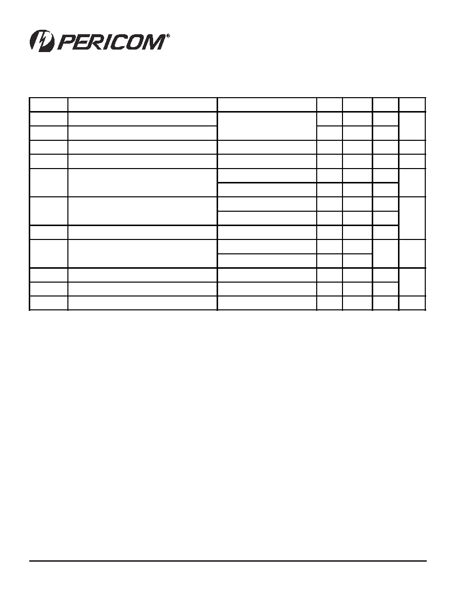
Recommended Operating Conditions
Function Table
H = High level
L = Low level
X = Irrelevent
Z = High-impedance (off)
? = Indeterminate
= Rising edge of clock
t
u
p
n
I
l
a
i
t
n
e
r
e
f
f
i
D
s
e
l
b
a
n
E
t
u
p
t
u
O
R
N
I
±
±
K
L
C
R
V
L
y
l
n
o
N
E
R
T
U
O
V
D
I
V
m
0
0
1
>
H
H
V
>
V
m
0
0
1
≠
D
I
V
m
0
0
1
>
H
?
V
D
I
V
m
0
0
1
<
H
L
X
X
L
Z
n
e
p
O
H
H
X
L
r
o
H
H
R
0
T
U
O
_
_
_
4
PS8664 02/21/03
12345678901234567890123456789012123456789012345678901234567890121234567890123456789012345678901212345678901234567890123456789012123456789012
12345678901234567890123456789012123456789012345678901234567890121234567890123456789012345678901212345678901234567890123456789012123456789012
PI90LV3810/PI90LVR3810
High-Speed Differential Line Receivers
Electrical Characteristics Over Recommended Operating Conditions
(unless otherwise noted)
Note: 1. All typical values are at 25∞C and with a 3.3V supply.
Symbol
Parameter
Test Conditions
Min.
Typ.
(1)
Max.
Units
V
ITH+
Positive-going differential input voltage threshold
100
mV
V
ITH-
Negative-going differential input voltage threshold
-100
V
OH
High-level output voltage
I
OH
= -8mA
2.4
3
V
V
OL
Low-level output voltage
I
OL
= 8mA
0.2
0.4
mV
I
CC
Supply current
Enabled, No load
22
40
mA
Disabled
3
I
I
Input current (R
IN
+ or R
IN
-inputs)
V
I
= 0V
-13
-20
µA
V
I
=
2.4V
-1.2
-3
I
I(OFF)
Power-off input current (R
IN
+ or R
IN
-inputs)
V
CC
=
0V, V
I
=
2.4V
12
± 20
I
IH
High-level input current (enables)
V
IH
=
2V
10
mA
V
IL
= 0.8V
I
IL
Low-level input current (enables)
V
O
= 0V
±1
µA
I
OZ
High-impedance output current
V
O
= 3.6V
10
C
IN
Input capacitance (R
IN
+ or R
IN
- inputs to GND
V
ID
= 0.4 sin 2.5E09t V
5
10
pF

5
PS8664 02/21/03
12345678901234567890123456789012123456789012345678901234567890121234567890123456789012345678901212345678901234567890123456789012123456789012
12345678901234567890123456789012123456789012345678901234567890121234567890123456789012345678901212345678901234567890123456789012123456789012
PI90LV3810/PI90LVR3810
High-Speed Differential Line Receivers
Switching Characteristics Over Recommended Operating Conditions
(unless otherwise noted)
l
o
b
m
y
S
r
e
t
e
m
a
r
a
P
s
n
o
i
t
i
d
n
o
C
t
s
e
T
.
n
i
M
.
p
y
T
)
1
(
.
x
a
M
s
t
i
n
U
t
H
L
P
t
u
p
t
u
o
l
e
v
e
l
-
h
g
i
h
-
o
t
-
w
o
l
,
e
m
it
y
a
l
e
d
n
o
it
a
g
a
p
o
r
P
2
e
r
u
g
i
F
e
e
S
)
0
1
8
3
V
L
0
9
I
P
(
1
6
.
2
4
s
n
t
L
H
P
t
u
p
t
u
o
l
e
v
e
l
-
w
o
l
-
o
t
-
h
g
i
h
,
e
m
it
y
a
l
e
d
n
o
it
a
g
a
p
o
r
P
5
.
2
t
r
e
m
it
e
s
i
r
l
a
n
g
i
s
t
u
p
t
u
o
l
a
it
n
e
r
e
f
fi
D
0
0
5
0
0
8
0
0
4
1
s
p
t
f
e
m
it
ll
a
f
l
a
n
g
i
s
t
u
p
t
u
o
l
a
it
n
e
r
e
f
fi
D
t
)
p
(
k
s
t
(
w
e
k
s
e
s
l
u
P
L
H
P
t
≠
H
L
P
)
0
5
1
0
0
6
t
)
o
(
k
s
w
e
k
s
t
u
p
t
u
O
)
2
(
0
0
1
0
5
4
t
)
p
p
(
k
s
w
e
k
s
t
r
a
p
-
o
t
-
t
r
a
P
)
3
(
1
s
n
t
H
Z
P
t
u
p
t
u
o
l
e
v
e
l
-
h
g
i
h
-
o
t
-
e
c
n
a
d
e
p
m
i
-
h
g
i
h
,
e
m
it
y
a
l
e
d
n
o
it
a
g
a
p
o
r
P
3
e
r
u
g
i
F
e
e
S
)
4
(
7
5
1
t
L
Z
P
t
u
p
t
u
o
l
e
v
e
l
-
w
o
l
-
o
t
-
e
c
n
a
d
e
p
m
i
-
h
g
i
h
,
e
m
it
y
a
l
e
d
n
o
it
a
g
a
p
o
r
P
t
Z
H
P
t
u
p
t
u
o
e
c
n
a
d
e
p
m
i
-
h
g
i
h
-
o
t
-l
e
v
e
l
-
h
g
i
h
,
e
m
it
y
a
l
e
d
n
o
it
a
g
a
p
o
r
P
t
Z
L
P
t
u
p
t
u
o
e
c
n
a
d
e
p
m
i
-
h
g
i
h
-
o
t
-l
e
v
e
l
-
w
o
l
,
e
m
it
y
a
l
e
d
n
o
it
a
g
a
p
o
r
P
t
U
S
K
L
C
e
r
o
f
e
b
a
t
a
d
,
e
m
it
p
u
-
t
e
S
0
1
8
3
R
V
L
0
9
I
P
2
.
1
t
H
K
L
C
r
e
tf
a
a
t
a
d
,
e
m
it
p
u
-
d
l
o
H
0
.
1
t
W
W
O
L
r
o
H
G
I
H
K
L
C
,
n
o
it
a
r
u
D
e
s
l
u
P
2
.
1
t
,
H
L
P
t
L
H
P
R
o
t
K
L
C
,
e
m
it
y
a
l
e
d
n
o
it
a
g
a
p
o
r
P
T
U
O
2
.
0
5
.
3
f
X
A
M
y
c
n
e
u
q
e
r
f
k
c
o
l
C
m
u
m
i
x
a
M
0
0
3
z
H
M
Notes:
1. All typical values are at 25∞C and with a 3.3V supply
2. t
sk(o)
is the magnitude of the time difference between the t
PLH
or t
PHL
of all drivers of a single device with all of their inputs
connected together.
3. t
sk(pp)
is the magnitude of the difference in propagation delay times between any specified terminals of two devices when both
devices operate with the same supply voltages, at the same temperature, and have identical packages and test circuits.
4. R
OUT0
disable time is 1 nanosecond greater.
6
PS8664 02/21/03
12345678901234567890123456789012123456789012345678901234567890121234567890123456789012345678901212345678901234567890123456789012123456789012
12345678901234567890123456789012123456789012345678901234567890121234567890123456789012345678901212345678901234567890123456789012123456789012
PI90LV3810/PI90LVR3810
High-Speed Differential Line Receivers
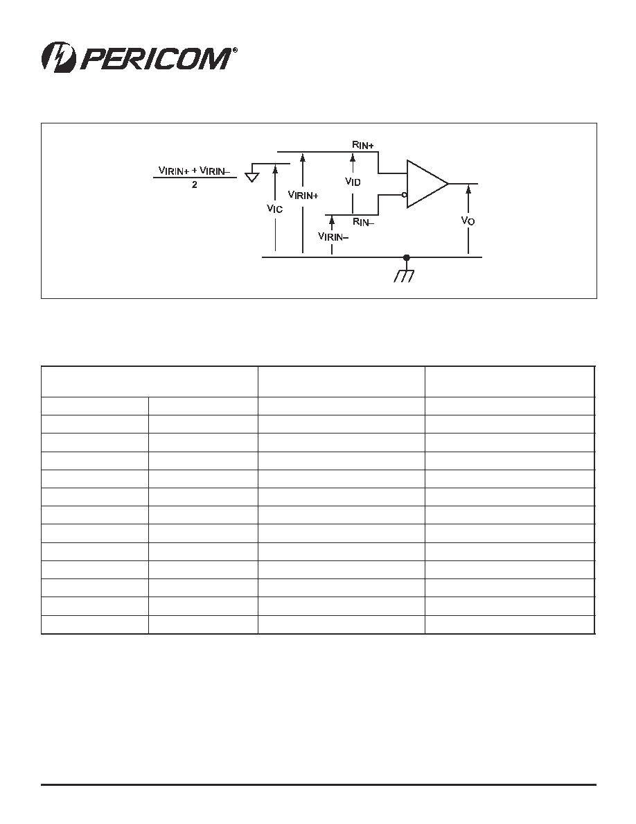
Figure 1. Voltage Definitions
s
e
g
a
t
l
o
V
d
e
il
p
p
A
l
a
i
t
n
e
r
e
f
f
i
D
g
n
i
t
l
u
s
e
R
e
g
a
t
l
o
V
t
u
p
n
I
-
n
o
m
m
o
C
g
n
i
t
l
u
s
e
R
e
g
a
t
l
o
V
t
u
p
n
I
e
d
o
M
V
+
N
I
R
I
V
≠
N
I
R
I
V
D
I
V
C
I
V
5
2
.
1
V
5
1
.
1
V
m
0
0
1
V
2
.
1
V
5
1
.
1
V
5
2
.
1
V
m
0
0
1
≠
V
2
.
1
V
4
.
2
V
3
.
2
V
m
0
0
1
V
5
3
.
2
V
3
.
2
V
4
.
2
V
m
0
0
1
≠
V
5
3
.
2
V
1
.
0
V
0
V
m
0
0
1
V
5
0
.
0
V
0
V
1
.
0
V
m
0
0
1
≠
V
5
0
.
0
V
5
.
1
V
9
.
0
V
m
0
0
6
V
2
.
1
V
9
.
0
V
5
.
1
V
m
0
0
6
≠
V
2
.
1
V
4
.
2
V
8
.
1
V
m
0
0
6
V
1
.
2
V
8
.
1
V
4
.
2
V
m
0
0
6
≠
V
1
.
2
V
6
.
0
V
0
V
m
0
0
6
V
3
.
0
V
0
V
6
.
0
V
m
0
0
6
≠
V
3
.
0
Parameter Measurement Information
Table 1. Receiver Minimum and Maximum Input Threshold Test Voltages

7
PS8664 02/21/03
12345678901234567890123456789012123456789012345678901234567890121234567890123456789012345678901212345678901234567890123456789012123456789012
12345678901234567890123456789012123456789012345678901234567890121234567890123456789012345678901212345678901234567890123456789012123456789012
PI90LV3810/PI90LVR3810
High-Speed Differential Line Receivers
Note:
1. All input pulses are supplied by a generator having the following characteristics: t
r
or t
f
1ns, Pulse Repetition
Rate (PRR) = 50 Mpps, Pulse width = 10 ±0.2ns. C
L
includes instrumentation and fixture capacitance within 0.06m
of the D.U.T.
Figure 2. Timing Test Circuit and Waveforms
Parameter Measurement Information

8
PS8664 02/21/03
12345678901234567890123456789012123456789012345678901234567890121234567890123456789012345678901212345678901234567890123456789012123456789012
12345678901234567890123456789012123456789012345678901234567890121234567890123456789012345678901212345678901234567890123456789012123456789012
PI90LV3810/PI90LVR3810
High-Speed Differential Line Receivers
Figure 3. Enable/Disable Test Circuit and Waveforms
Parameter Measurement Information
Note:
1. All input pulses are supplied by a generator having the following characteristics: t
r
or t
f
1ns, Pulse Repetition
Rate (PRR) = 0.5 Mpps, pulse width = 500 ±10ns. C
L
includes instrumentation and fixture capacitance within 0.06m
of the D.U.T.

9
PS8664 02/21/03
12345678901234567890123456789012123456789012345678901234567890121234567890123456789012345678901212345678901234567890123456789012123456789012
12345678901234567890123456789012123456789012345678901234567890121234567890123456789012345678901212345678901234567890123456789012123456789012
PI90LV3810/PI90LVR3810
High-Speed Differential Line Receivers
0
0.1
0.2
0.3
≠70
≠60
≠50
≠40
≠30
≠20
≠10
0
0
5.0
4.5
4.0
3.5
3.0
2.5
2.0
1.5
1.0
0.5
0
10
20
30
40
50
60
70
80
0.4
0.5
0.6
20
0
40
60
80 100 120 140 160 180 200
2.5
200
180
160
140
120
100
80
60
40
20
0
2.0
Max at V
CC
= 3V
Minimum
V
ID
≠ Differential Input Voltage ≠ V
I
OH
≠ High-Level Output Current ≠ mA
I
OL
≠ Low-Level Output Current ≠ mA
f ≠ Switching Frequency ≠ MHz
Max at V
CC
>3.15V
V
CC
= 3.6V
V
CC
= 3.3V
I
CC
≠ Supply Current ≠ mA
V
OL
≠ Lo
w-Le
v
el Output
V
oltage ≠
V
V
IC
≠ Common-Moce Input
V
oltate ≠
V
V
OH
≠ High-Le
v
el Output
V
oltate ≠
V
V
CC
= 3V
1.5
1.0
0.5
4.0
3.5
3.0
2.5
2.0
1.5
1.0
0.5
0
0
Typical Characteristics
Figure 4. Common-Mode Input Voltage
vs.
Differential Input Voltage
Figure 5. Supply Current
vs.
Switching Frequency
Figure 6. High-Level Output Voltage
vs.
High-Level Output Current
Figure 7. Low-Level Output Voltage
vs.
Low-Level Output Current

1 0
PS8664 02/21/03
12345678901234567890123456789012123456789012345678901234567890121234567890123456789012345678901212345678901234567890123456789012123456789012
12345678901234567890123456789012123456789012345678901234567890121234567890123456789012345678901212345678901234567890123456789012123456789012
PI90LV3810/PI90LVR3810
High-Speed Differential Line Receivers
3.0
2.9
2.8
2.7
2.6
2.5
2.4
2.3
2.2
2.1
≠50
≠30
Ta ≠ Free-Air Temperature ≠ ∞C
V
CC
= 3V
V
CC
= 3.6V
V
CC
= 3.3V
t
PLH
≠ Lo
w-to-High Propagation Dela
y
Time ≠ ns
≠10
10
30
50
70
90
2
3.0
2.9
2.8
2.7
2.6
2.5
2.4
2.3
2.2
2.1
≠50
≠30
Ta ≠ Free-Air Temperature ≠ ∞C
V
CC
= 3V
V
CC
= 3.6V
V
CC
= 3.3V
t
PHL
≠ High-to-Lo
w Propagation Dela
y
Time ≠ ns
≠10
10
30
50
70
90
2
Typical Characteristics
Figure 8. Low-to-High Propagation Delay Time
vs.
Free-Air Temperature
Figure 9. High-to-Low Propagation Delay Time
vs.
Free-Air Temperature

1 1
PS8664 02/21/03
12345678901234567890123456789012123456789012345678901234567890121234567890123456789012345678901212345678901234567890123456789012123456789012
12345678901234567890123456789012123456789012345678901234567890121234567890123456789012345678901212345678901234567890123456789012123456789012
PI90LV3810/PI90LVR3810
High-Speed Differential Line Receivers
Packaging Mechanical: 48-Pin TSSOP (A)
Pericom Semiconductor Corporation
2380 Bering Drive ∑ San Jose, CA 95131 ∑ 1-800-435-2336 ∑ Fax (408) 435-1100 ∑ http://www.pericom.com
Ordering Information
e
d
o
C
g
n
i
r
e
d
r
O
e
m
a
N
e
g
a
k
c
a
P
e
p
y
T
e
g
a
k
c
a
P
e
g
n
a
R
g
n
i
t
a
r
e
p
O
A
0
1
8
3
V
L
0
9
I
P
8
4
A
)
A
(
P
O
S
S
T
n
i
p
-
8
4
C
∞
5
8
o
t
C
∞
0
4
≠
A
0
1
8
3
R
V
L
0
9
I
P
8
4
A
)
A
(
P
O
S
S
T
n
i
p
-
8
4
C
∞
5
8
o
t
C
∞
0
4
≠
.236
.244
.488
.496
.002
.006
SEATING PLANE
.007
.010
.0197
BSC
.004
.008
.319
1
48
12.4
12.6
6.0
6.2
0.50
0.17
0.27
8.1
0.05
0.15
0.09
0.20
X.XX
X.XX
DENOTES DIMENSIONS
IN MILLIMETERS
.018
.030
0.45
0.75
.047
1.20 Max
BSC