
1
PS8659B 09/28/04
Features
∑ Meets or Exceeds the Requirements of ANSI
TIA/EIA-644-1995 Standard
∑ Signaling rates up to 400 Mbps
∑ Interfaces to LVDS, LVPECL
∑ Bus-Terminal ESD exceeds 10kV
∑ Differential Input Voltage Threshold less than 100mV
∑ Typical Propagation Delay Times of 2.6ns
∑ Typical Power Dissipation of 40mW @200 MHz
∑ Low Voltage TTL (LVTTL) Level is 5V Tolerant
∑ Open-Circuit Fail Safe
∑ Output are High Impedance with V
CC
<1.5V
∑ Integrated 110-ohm Line Termination Resistor (PI90LVT02)
∑ Operates from a 3.3V supply
∑ Input common-mode voltage range 0V≠3.2V
∑ Industrial Temperature Operating Range: ≠40∞C to 85∞C
∑ Packaging (Pb-free & Green available):
- 5-pin space-saving SOT-23 (T)
12345678901234567890123456789012123456789012345678901234567890121234567890123456789012345678901212345678901234567890123456789012123456789012
12345678901234567890123456789012123456789012345678901234567890121234567890123456789012345678901212345678901234567890123456789012123456789012
PI90LV02/PI90LVT02
SOTiny
TM
LVDS High-Speed
Differential Line Receiver
s
t
u
p
n
I
s
t
u
p
t
u
O
V
D
I
V
=
A
V
≠
B
R
T
U
O
V
D
I
V
m
0
5
>
H
V
<
V
m
0
5
≠
D
I
V
m
0
5
<
?
V
D
I
V
m
0
5
≠
L
n
e
p
O
H
Description
The PI90LV02 and PI90LVT02 are single differential line receivers
that use low-voltage differential signaling (LVDS) to support data
rates up to 400 Mbps. These products are designed for applications
requiring high-speed, low-power consumption, low-noise genera-
tion, and a small package.
A differential input signal (350mV) is translated by the device to a
3.3V CMOS output level. The PI90LVT02 integrates the terminating
resistor while the PI90LV02 requires an external resistor.
Applications
Applications include point-to-point and multi-drop baseband data
transmissions over impedance media of approximately 100-ohms.
The transmission media can be printed circuit board traces,
backplanes, or cables.
The PI90LV02 and PI90LVT02 and companion line drivers (PI90LV01
and PI90LVB01) provide new alternatives to RS-232, PECL, and ECL
devices for high-speed, point-to-point interface applications.
H = high level
L = low level
? = indeterminate
Logic Diagram
Function Table
Pinout
5
3
A
4
B
ROUT
PI90LV02
5
3
A
4
110-ohm
B
ROUT
PI90LVT02
1
2
3
VCC
GND
A
ROUT
B
5
4
12345678901234567890123456789012123456789012345678901234567890121234567890123456789012345678901212345678901234567890123456789012123456789012
12345678901234567890123456789012123456789012345678901234567890121234567890123456789012345678901212345678901234567890123456789012123456789012
PI90LV02/PI90LVT02
SOTiny
TM
LVDS High-Speed Differential Line Receiver
2
PS8659B 09/28/04
Supply Voltage Range, V
CC
(1) ..................................................................................
≠0.5V to 4V
Voltage Range (A, B , or R
OUT
) ...................................................... ≠0.5 to V
CC
+0.5V
ESD rating (HBM, 1.5K-ohms, 100pF) ............................................................
10KV
Continuous total power dissipation ................................. See dissipation rating table
Storage Temperature Range ................................................................ ≠65∞C to 150∞C
Lead Temperature 1.6 mm (1/16 inch) from case for 10 seconds ......................... 250∞C
Absolute Maximum Ratings Over Operating Free-Air Temperature
(unless otherwise noted)
Stresses beyond those listed under "Absolute Maximum Ratings" may cause permanent damage to the
device. These are stress ratings only, and functional operation of the device at these or any other conditions
beyond those indicated under "Recommended Operating Conditions" is not implied. Exposure to Absolute-
Maximum-Rated conditions for extended periods may affect device reliability.
Recommended Operating Conditions
.
n
i
M
.
m
o
N
.
x
a
M
s
t
i
n
U
V
,
e
g
a
tl
o
V
y
l
p
p
u
S
C
C
0
.
3
3
.
3
6
.
3
V
V
|
,
e
g
a
tl
o
v
t
u
p
n
i
l
a
it
n
e
r
e
f
fi
d
f
o
e
d
u
ti
n
g
a
M
D
I
|
1
.
0
6
.
0
V
,
e
g
a
tl
o
V
t
u
p
n
I
e
d
o
M
-
n
o
m
m
o
C
C
I
)
6
e
r
u
g
i
F
e
e
S
(
0
V
|
D
I
|
≠
≠
≠
≠
0
.
2
2
V
C
C
8
.
0
≠
T
,
e
r
u
t
a
r
e
p
m
e
t
ri
a
-
e
e
r
f
g
n
it
a
r
e
p
O
A
0
4
≠
5
8
C
∞
e
g
a
k
c
a
P
T
A
g
n
i
t
a
R
r
e
w
o
P
C
∞
5
2
£
T
e
v
o
b
A
r
o
t
c
a
F
g
n
i
t
a
r
e
D
A
C
∞
5
2
=
*
*
T
A
g
n
i
t
a
R
r
e
w
o
P
C
∞
5
8
=
)
T
(
3
2
-
T
O
S
n
i
P
-
5
W
m
5
8
3
C
∞
/
W
m
1
.
3
W
m
0
0
2
Dissipation Rating Table
**This is the inverse of the junction-to-ambient thermal resistance when board-mounted (low-K) and with no air flow.
Notes:
1. All voltage values, except differential I/O bus voltages, are with respect to ground terminal.

12345678901234567890123456789012123456789012345678901234567890121234567890123456789012345678901212345678901234567890123456789012123456789012
PI90LV02/PI90LVT02
SOTiny
TM
LVDS High-Speed Differential Line Receiver
3
PS8659B 09/28/04
Figure 1. V
IC
vs. V
ID
and V
CC
l
o
b
m
y
S
r
e
t
e
m
a
r
a
P
s
n
o
i
t
i
d
n
o
C
t
s
e
T
.
n
i
M
.
p
y
T
)
1
(
.
x
a
M
s
t
i
n
U
V
+
H
T
I
d
l
o
h
s
e
r
h
t
e
g
a
tl
o
v
t
u
p
n
i
l
a
it
n
e
r
e
f
fi
d
g
n
i
o
g
-
e
v
it
i
s
o
P
1
e
l
b
a
T
&
,
2
e
r
u
g
i
F
e
e
S
0
0
1
V
m
V
≠
H
T
I
d
l
o
h
s
e
r
h
t
e
g
a
tl
o
v
t
u
p
n
i
l
a
it
n
e
r
e
f
fi
d
g
n
i
o
g
-
e
v
it
a
g
e
N
0
0
1
≠
V
H
O
e
g
a
tl
o
v
t
u
p
t
u
o
l
e
v
e
l
-
h
g
i
H
I
H
O
A
m
8
≠
=
4
.
2
3
V
V
L
O
e
g
a
tl
o
v
t
u
p
t
u
o
l
e
v
e
l
-
w
o
L
I
L
O
A
m
8
=
5
2
.
0
4
.
0
I
C
C
t
n
e
r
r
u
c
y
l
p
p
u
S
e
t
a
t
s
y
d
a
e
t
S
,
d
a
o
l
o
N
4
7
A
m
I
I
)
s
t
u
p
n
i
B
r
o
A
(
t
n
e
r
r
u
c
t
u
p
n
I
2
0
V
L
V
I
V
0
=
0
2
±
A
µ
2
0
T
V
L
V
I
n
e
p
o
t
u
p
n
i
r
e
h
t
O
,
V
0
=
0
4
±
2
0
V
L
V
I
V
r
o
V
4
.
2
=
C
C
8
.
0
≠
2
.
1
≠
2
0
T
V
L
V
I
n
e
p
o
t
u
p
n
i
r
e
h
t
O
,
V
4
.
2
=
4
.
2
≠
I
D
I
t
n
e
r
r
u
c
t
u
p
n
i
l
e
v
e
l
-
h
g
i
H
I
(
A
I
I
≠
B
I
)
2
0
V
L
V
A
I
V
,
V
0
=
B
I
V
1
.
0
=
V
A
I
V
,
V
4
.
2
=
B
I
V
3
.
2
=
2
±
2
0
T
V
L
V
A
I
V
,
V
4
.
2
=
B
I
V
3
.
2
=
5
.
1
8
.
1
2
.
2
A
m
I
)
F
F
O
(
I
t
n
e
r
r
u
c
t
u
p
n
i
f
f
o
-
r
e
w
o
P
)
s
t
u
p
n
i
B
r
o
A
(
2
0
V
L
V
C
C
V
,
V
0
=
I
V
4
.
2
=
0
2
A
µ
2
0
T
V
L
V
C
C
V
,
V
0
=
I
,
V
4
.
2
=
n
e
p
o
t
u
p
n
i
r
e
h
t
O
0
4
Electrical Characteristics, V
CC
= 3V to 3.6V
(Over Recommended Operating Conditions, unless otherwise noted).
I VID I ≠ Differential Input Voltage ≠ V
3
2.5
2
1.5
1
0.5
0
0
0.1
0.2
VCC = 3.6V
COMMON-MODE INPUT VOLTAGE
vs.
DIFFERENTIAL INPUT VOLTAGE
VCC = 3.6V
VCC = 3.6V
0.3
0.4
0.5
0.6
0.7
0.8
V
IC
≠ Common-Mode Input
V
oltage ≠
V
12345678901234567890123456789012123456789012345678901234567890121234567890123456789012345678901212345678901234567890123456789012123456789012
12345678901234567890123456789012123456789012345678901234567890121234567890123456789012345678901212345678901234567890123456789012123456789012
PI90LV02/PI90LVT02
SOTiny
TM
LVDS High-Speed Differential Line Receiver
4
PS8659B 09/28/04
Notes:
1. All typical values are at 25∞C and with a 3.3V supply
2. t
sk(p)
is the magnitude of the time difference between the high-to-low and low-to-high propagation delay times at an output.
Receiver Switching Characteristics, V
CC
= 3V to 3.6V
(Over Recommended Operating Conditions, unless noted).
l
o
b
m
y
S
r
e
t
e
m
a
r
a
P
s
n
o
i
t
i
d
n
o
C
t
s
e
T
.
n
i
M
.
p
y
T
)
1
(
.
x
a
M
s
t
i
n
U
t
H
L
P
t
u
p
t
u
o
l
e
v
e
l
h
g
i
h
-
o
t
-
w
o
l
,
e
m
it
y
a
l
e
d
n
o
it
a
g
a
p
o
r
P
C
L
,
F
p
0
1
=
3
e
r
u
g
i
F
e
e
S
3
.
1
1
.
2
2
.
3
s
n
t
L
H
P
t
u
p
t
u
o
l
e
v
e
l
w
o
l
-
o
t
-
h
g
i
h
,
e
m
it
y
a
l
e
d
n
o
it
a
g
a
p
o
r
P
3
.
1
0
.
2
2
.
3
t
r
e
m
it
e
s
i
r
l
a
n
g
i
s
t
u
p
t
u
O
7
.
0
4
.
1
t
f
e
m
it
ll
a
f
l
a
n
g
i
s
t
u
p
t
u
O
7
.
0
4
.
1
t
)
p
(
k
s
(
w
e
k
s
e
s
l
u
P
t
L
H
P
t
-
H
L
P
)
)
2
(
1
.
0
5
.
0
t
H
Z
P
e
c
n
a
d
e
p
m
i
-
h
g
i
h
-
o
t
-l
e
v
e
l
-
h
g
i
h
,
e
m
it
y
a
l
e
d
n
o
it
a
g
a
p
o
r
P
t
u
p
t
u
o
4
e
r
u
g
i
F
e
e
S
5
.
1
1
.
3
t
L
Z
P
t
u
p
t
u
o
e
c
n
a
d
e
p
m
i
-
w
o
l
-
o
t
-l
e
v
e
l
-
w
o
l
,
e
m
it
y
a
l
e
d
n
o
it
a
g
a
p
o
r
P
0
.
4
0
.
6
t
Z
H
P
t
u
p
t
u
o
l
e
v
e
l
-
h
g
i
h
-
o
t
-
e
c
n
a
d
e
p
m
i
-
h
g
i
h
,
e
m
it
y
a
l
e
d
n
o
it
a
g
a
p
o
r
P
5
.
2
5
.
3
t
Z
L
P
t
u
p
t
u
o
l
e
v
e
l
-
h
g
i
h
-
o
t
-
e
c
n
a
d
e
p
m
i
-
w
o
l
,
e
m
it
y
a
l
e
d
n
o
it
a
g
a
p
o
r
P
0
.
6
6
.
7
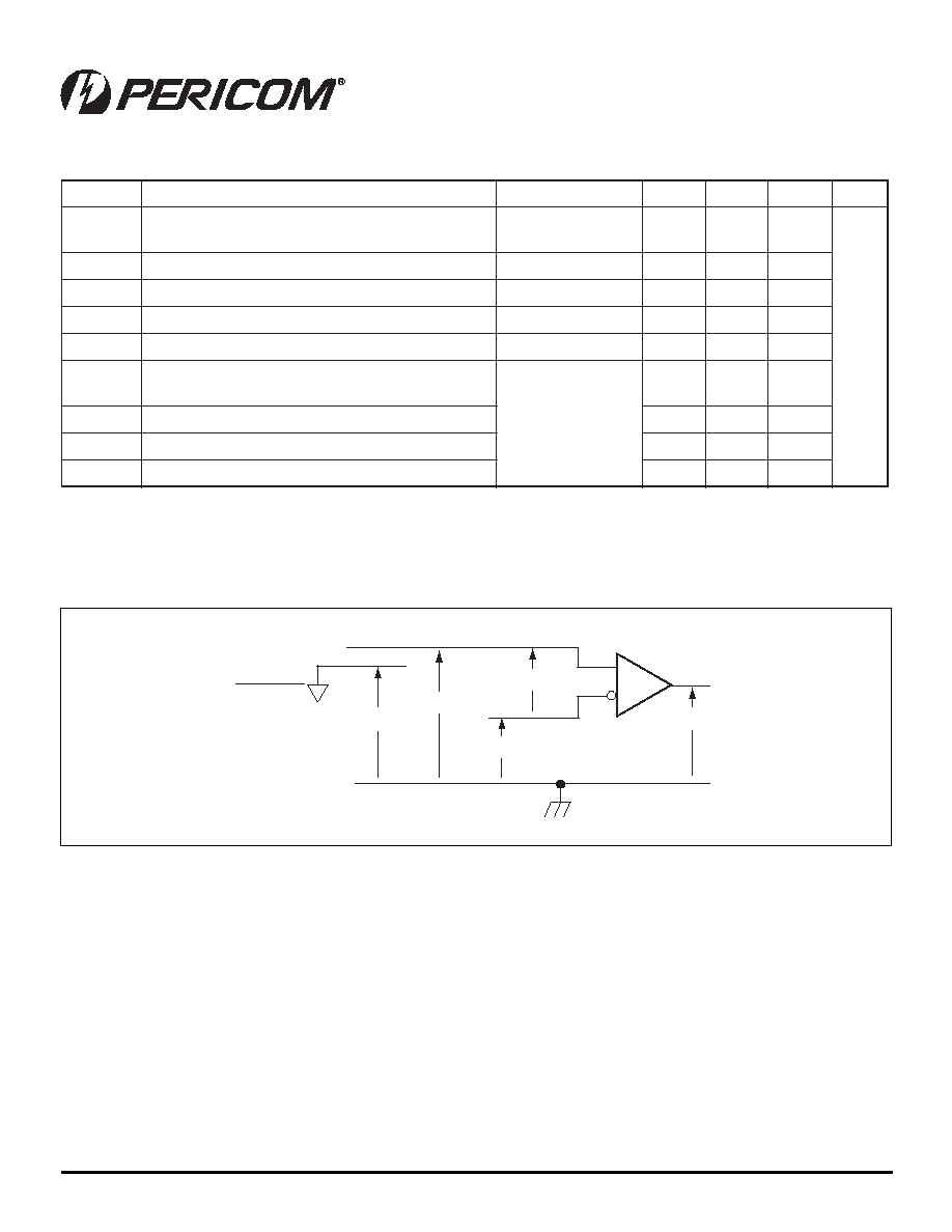
Parameter Measurement Information
Figure 2. Receiver Voltage Definitions
2
A
B
V
ID
R
OUT
V
O
V
IA
+ V
IB
V
IC
V
IB
V
IA

12345678901234567890123456789012123456789012345678901234567890121234567890123456789012345678901212345678901234567890123456789012123456789012
PI90LV02/PI90LVT02
SOTiny
TM
LVDS High-Speed Differential Line Receiver
5
PS8659B 09/28/04
)
V
(
s
e
g
a
t
l
o
V
d
e
il
p
p
A
l
a
i
t
n
e
r
e
f
f
i
D
g
n
i
t
l
u
s
e
R
)
V
m
(
e
g
a
t
l
o
V
t
u
p
n
I
e
d
o
M
-
n
o
m
m
o
C
g
n
i
t
l
u
s
e
R
)
V
(
e
g
a
t
l
o
V
t
u
p
n
I
V
A
I
V
B
I
V
D
I
V
C
I
5
2
.
1
0
2
.
1
0
5
2
.
1
5
1
.
1
0
2
.
1
0
5
≠
2
.
1
4
.
2
5
3
.
2
0
5
5
3
.
2
3
.
2
5
3
.
2
0
5
≠
5
3
.
2
5
0
.
0
0
0
5
5
0
.
0
0
5
0
.
0
0
5
≠
5
0
.
0
5
.
1
9
.
0
0
0
6
2
.
1
9
.
0
5
.
1
0
0
6
≠
2
.
1
4
.
2
8
.
1
0
0
6
1
.
2
8
.
1
4
.
2
0
0
6
≠
1
.
2
6
.
0
0
0
0
6
3
.
0
0
6
.
0
0
0
6
≠
3
.
0
Table 1. Receiver Minimum and Maximum Input Threshold Test Voltages

12345678901234567890123456789012123456789012345678901234567890121234567890123456789012345678901212345678901234567890123456789012123456789012
12345678901234567890123456789012123456789012345678901234567890121234567890123456789012345678901212345678901234567890123456789012123456789012
PI90LV02/PI90LVT02
SOTiny
TM
LVDS High-Speed Differential Line Receiver
6
PS8659B 09/28/04
C
L
10pF
1.4 V
t
PHL
t
f
t
f
With
V
CC
= 3.3V
t
PLH
80%
20%
Note A:
All input pulses are supplied by a generator having the following characteristics:
t
r
or t
f
1ns, pulse repetition rate (PRR) = 50 Mpps, pulse width = 10 ±0.2ns.
CL includes instrumentation and fixture capacitance within 0.06m of the D.U.T.
Note B:
To verify input max signalling rate, the input signal transition time (tr/tf) should not
exceeds 1.25ns.
VIA
VIB
VID
ROUT
VO
VIA
VIB
VID
1V
0.4V
0V
-0.4V
VO
VOH
1.4V
VOL
Figure 3. Timing Test Circuit and Waveforms

12345678901234567890123456789012123456789012345678901234567890121234567890123456789012345678901212345678901234567890123456789012123456789012
PI90LV02/PI90LVT02
SOTiny
TM
LVDS High-Speed Differential Line Receiver
7
PS8659B 09/28/04
Figure 4. Enable/Disable Time Test Circuit and Waveforms
V
O
C
L
10 pF
+
≠
500
1.2 V
B
A
EN
EN
EN
R
OUT
R
OUT
Inputs
V
TEST
NOTE A: All input pulses are supplied by a genertor having the following characteristics: tr or tf
1ns,
pulse repetition rate (PRR) = 0.5 Mpps, pulse wide = 500 ±10ns. CL includes instrumentation
and fixture capacitance within 0.06m of the D.U.T.
NOTE B: To verify input max signalling rate, the input signal transition time (tr/tf) should not
exceeds 1.25ns.
t
PZL
V
TEST
t
PZL
t
PLZ
2.5 V
1.4 V
V
OL
+0.5 V
V
OL
2 V
1.4 V
0.8 V
2.5 V
1 V
t
PZH
A
V
TEST
t
PZH
t
PHZ
V
OH
1.4 V
V
OH
≠0.5 V
0 V
2 V
1.4 V
0.8 V
0 V
1.4 V
B

12345678901234567890123456789012123456789012345678901234567890121234567890123456789012345678901212345678901234567890123456789012123456789012
12345678901234567890123456789012123456789012345678901234567890121234567890123456789012345678901212345678901234567890123456789012123456789012
PI90LV02/PI90LVT02
SOTiny
TM
LVDS High-Speed Differential Line Receiver
8
PS8659B 09/28/04
Figure 5
Figure 6
Figure 7
Figure 8
HIGH-LEVEL OUTPUT VOLTAGE
VS.
HIGH-LEVEL OUTPUT CURRENT
4
V
CC
= 3.3V
V
CC
= 2.7V
3.5
3
2.5
2
1.5
1
0.5
0
≠70
≠60
≠50
≠40
IOH - High-Level Output Current - mA
V
OH
- High-Le
v
el Output
V
oltage -
V
≠30
≠20
≠10
0
LOW-LEVEL OUTPUT VOLTAGE
VS.
LOW-LEVEL OUTPUT CURRENT
4
V
CC
= 2.7V
V
CC
= 3.3V
3.5
3
2.5
2
1.5
1
0.5
0
0
10
20
30
IOL - Low-Level Output Current - mA
V
OL
- Lo
w-Le
v
el Output
V
oltage -
V
40
50
60
70
HIGH-TO-LOW LEVEL
PROPAGATION DELAY TIME
VS.
FREE-AIR TEMPERATURE
t
PHL
- High-to-Lo
w
Le
vel Pr
opa
gation Dela
y
Time - ns
2.85
2.9
V
CC
= 2.4V
V
CC
= 3V
V
CC
= 3.6V
V
CC
= 3.3V
V
CC
= 2.7V
2.8
2.75
2.7
2.65
2.6
2.55
2.5
2.45
2.4
≠40
≠20
0
20
TA - Free-Air Temperature - ∞C
40
60
80
100
LOW-TO-HIGH LEVEL
PROPAGATION DELAY TIME
VS.
FREE-AIR TEMPERATURE
t
PLH
- Lo
w-to-High Le
vel Pr
opa
gation Dela
y
Time - ns
V
CC
= 2.4V
V
CC
= 3V
V
CC
= 3.3V
V
CC
= 3.6V
V
CC
= 2.7V
3
2.9
2.8
2.7
2.6
2.5
2.4
2.3
2.2
≠40
≠20
0
20
TA - Free-Air Temperature - ∞C
40
60
80
100

12345678901234567890123456789012123456789012345678901234567890121234567890123456789012345678901212345678901234567890123456789012123456789012
PI90LV02/PI90LVT02
SOTiny
TM
LVDS High-Speed Differential Line Receiver
9
PS8659B 09/28/04
Packaging Mechanical: 5-Pin SOT-23 (T)
.102
.118
BSC
0.60
1
2
3
.000
.005
0.00
0.15
.014
.019
0.35
0.50
5
4
1.50
1.75
.059
.068
0.10
.023
.004
1.45 MAX.
SEATING
PLANE
.057
0" - 10"
1.90
.075
.037
BSC
2.60
3.00
0.95
.110
.118
2.80
3.00
X.XX
X.XX
Datum "A"
DENOTES DIMENSIONS
IN MILIMETERS
Pericom Semiconductor Corporation ∑ 1-800-435-2336 ∑ www.pericom.com
Ordering Information
Notes:
1. Thermal characteristics can be found on the company web site at www.pericom.com/packaging/
2. X = Tape and reel
Ordering Code
Package Code
Package Description
Top Marking
PI90LV02TX
T
5-pin, SOT23
L5
PI90LV02TEX
T
Pb-free & Green, 5-pin, SOT23
L5
PI90LVT02TX
T
5-pin, SOT23
L6
PI90LVT02TEX
T
Pb-free & Green, 5-pin, SOT23
L6