 | ÐлекÑÑоннÑй компоненÑ: PS4066CEE | СкаÑаÑÑ:  PDF PDF  ZIP ZIP |
Äîêóìåíòàöèÿ è îïèñàíèÿ www.docs.chipfind.ru
1
PS8184A 10/15/98
Features
·
Low On-Resistance
·
On-Resistance Matching Between Channels, 0.2
typ
·
On-Resistance Flatness, <2
typ
·
Low Off-Channel Leakage, <100pA @ +25oC
·
TTL/CMOS Logic Compatible
·
GND-to-V+ Analog Signal Dynamic Range
·
Low Power Consumption (<12
µ
W)
·
Low Crosstalk: -86dB @ 1MHz
·
Low Off-Isolation: -58dB @ 1 MHz
·
Wide Bandwidth: > 100 MHz
·
Small QSOP-16 Package Saves Board Area
Applications
·
Instrumentation, ATE
·
Sample-and-Holds
·
Audio Switching and Routing
·
Telecommunication Systems
·
PBX, PABX
·
Battery-Powered Systems
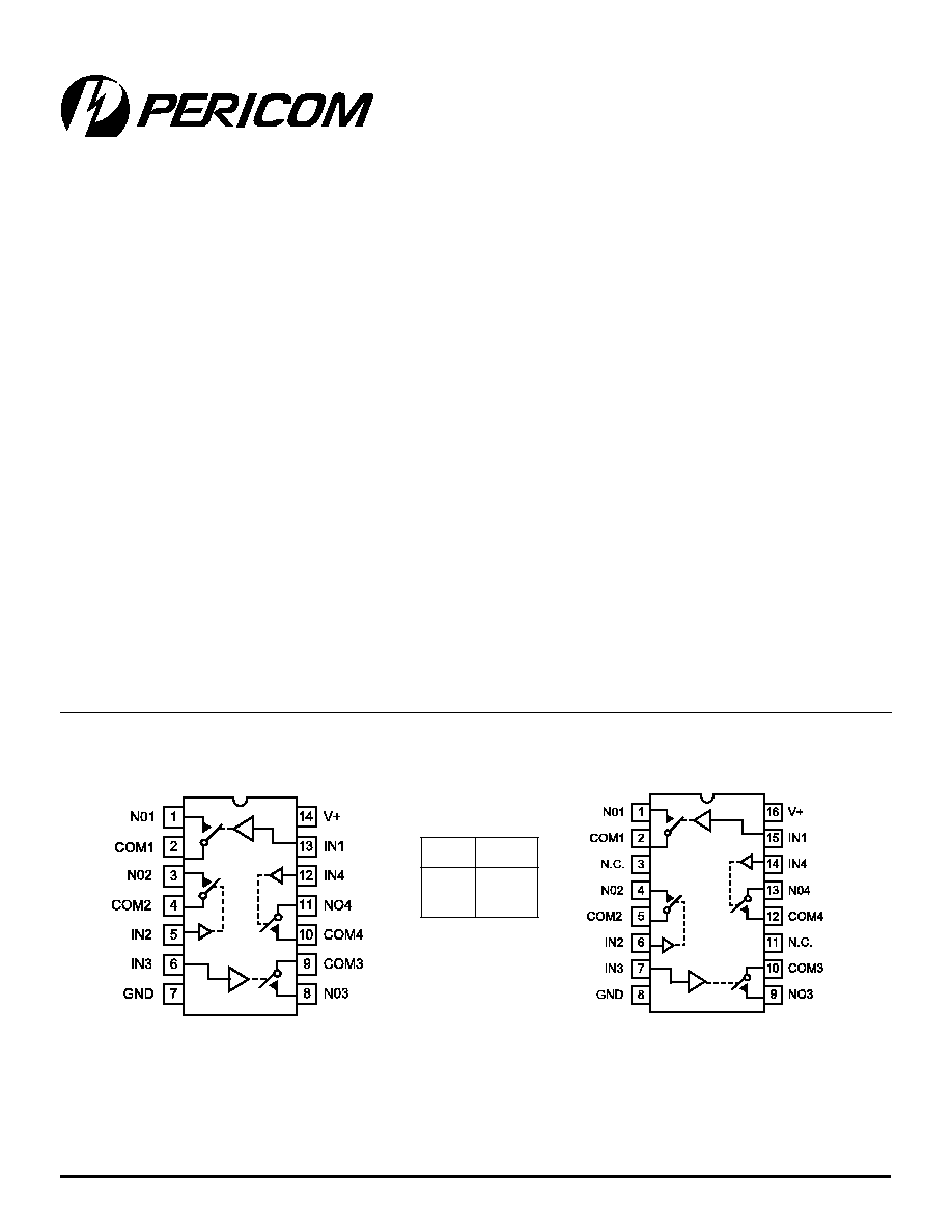
N.C. = No Internal Connection
Switches shown for logic "0" input
Description
The PS4066/PS4066A are improved SPST CMOS analog
switches ideal for low-distortion audio switching. These high pre-
cision, medium voltage switches were designed to operate with
single-supplies from +3V to 16V. They are fully specified with
+12V, +5V, and +3V supplies. The PS4066/PS4066A has four
normally open (NO) switches. Each switch conducts current
equally well in either direction when on. In the off state each
switch blocks voltages up to the power-supply rails.
With +12V power supply, the PS4066/PS4066A guarantee <45
on-resistance. On-resistance matching between channels is within
2
(PS4066). On-resistance flatness is less than 4
(PS4066A)
over the specified range. The PS4066A guarantees low leakage
currents (<100pA @ 25oC, <6nA @ +85oC) and fast switching
speeds (tON < 175ns). ESD sensitivity rating is >2,000V per
MIL-STD 883, Method 3015.7
Both devices are available in PDIP-14, narrow-body SOIC-14,
and QSOP-16 packages. Available temperature ranges are: com-
mercial (0oC to 70oC), and industrial (-40oC to +85oC).
For operation below 5V, the PI5A101/PI5A391/PI5A392 are also
recommended.
Top View
Functional Diagrams, Pin Configurations, and Truth Table
c
i
g
o
L
h
c
ti
w
S
0
1
F
F
O
N
O
Top View
QSOP
PDIP/SO
PS4066/PS4066A
Low-Cost, Quad, SPST, CMOS Analog Switches
12345678901234567890123456789012123456789012345678901234567890121234567890123456789012345678901212345678901234567890123456789012123456789012
12345678901234567890123456789012123456789012345678901234567890121234567890123456789012345678901212345678901234567890123456789012123456789012
12345678901234567890123456789012123456789012345678901234567890121234567890123456789012345678901212345678901234567890123456789012123456789012
2
PS8184A 10/15/98
PS4066/PS4066A
Low-Cost, Quad, SPST, CMOS Analog Switches
Absolute Maximum Ratings
Caution: Stresses beyond those listed under "Absolute Maximum Ratings" may cause permanent damage to the device. This is a stress only
rating and operation of the device at these or any other conditions beyond those indicated in the operational sections of this specification is not
implied.
Electrical Specifications - Single +12V Supply
(V+ = 12V ±10%, GND = 0V, V
INH
= 4V, V
INL
= 0.8V)
r
e
t
e
m
a
r
a
P
l
o
b
m
y
S
s
n
o
it
i
d
n
o
C
)
C
°
(
.
p
m
e
T
n
i
M
(1)
p
y
T
(2)
x
a
M
(1)
s
ti
n
U
h
c
ti
w
S
g
o
l
a
n
A
l
a
n
g
i
S
g
o
l
a
n
A
e
g
n
a
R
)
3
(
V
G
O
L
A
N
A
ll
u
F
0
+
V
V
e
c
n
a
t
si
s
e
R
n
O
R
N
O
I
,
V
2
1
=
+
V
M
O
C
,
A
m
2
=
V
O
N
V
0
1
=
5
2
2
1
5
4
ll
u
F
5
5
h
c
t
a
M
e
c
n
a
t
si
s
e
R
-
n
O
sl
e
n
n
a
h
C
n
e
e
w
t
e
B
)
4
(
R
N
O
I
,
V
2
1
=
+
V
M
O
C
A
m
2
=
V
O
N
V
0
1
=
6
6
0
4
S
P
A
6
6
0
4
S
P
5
2
5
.
0
5
.
0
4
2
ll
u
F
6
e
c
n
a
t
si
s
e
R
-
n
O
s
s
e
n
t
al
F
)
5
(
R
)
N
O
(
T
A
L
F
I
,
V
2
1
=
+
V
M
O
C
,
A
m
2
=
V
O
N
V
1
,
V
5
,
V
0
1
=
5
2
2
4
ll
u
F
6
ff
O
C
N
r
o
O
N
t
n
e
rr
u
C
e
g
a
k
a
e
L
)
6
(
I
)
F
F
O
(
O
N
OR
I
)
F
F
O
(
C
N
V
,
V
2
1
=
+
V
M
O
C
,
V
0
=
V
O
N
V
0
1
=
6
6
0
4
S
P
A
6
6
0
4
S
P
5
2
1
-
1
.
0
-
1
1
.
0
A
n
ll
u
F
6
-
6
e
g
a
k
a
e
L
ff
O
M
O
C
t
n
e
rr
u
C
)
6
(
I
)
F
F
O
(
M
O
C
V
,
V
2
1
=
+
V
M
O
C
,
V
0
=
V
O
N
V
0
1
=
6
6
0
4
S
P
A
6
6
0
4
S
P
5
2
1
-
1
.
0
-
1
1
.
0
ll
u
F
6
-
6
e
g
a
k
a
e
L
n
O
M
O
C
t
n
e
rr
u
C
)
6
(
I
)
N
O
(
M
O
C
V
,
V
2
1
=
+
V
M
O
C
,
V
0
1
=
V
O
N
V
0
1
=
6
6
0
4
S
P
A
6
6
0
4
S
P
5
2
2
-
2
.
0
-
2
2
.
0
ll
u
F
2
1
-
2
1
Thermal Information
Continuous Power Dissipation (T
A
= +70
º
C)
Plastic DIP (derate 10.5mW/
º
C above +70
º
C) . . . . . . 800mW
SO and QSOP (derate 8.7mW/
º
C above +70
º
C) . . . . . 650mW
Storage Temperature . . . . . . . . . . . . . . . . . . . -65
º
C to +150
º
C
Lead Temperature (soldering, 10s) . . . . . . . . . . . . . . . +300
º
C
Note
Signals on NC, NO, COM, or IN exceeding V+ or GND are
clamped by internal diodes. Limit forward diode current to 30mA.
Voltages Referenced to GND
V+ . . . . . . . . . . . . . . . . . . . . . . . . . . . . . . . . . . -0.3V to +17V
V
IN
, V
COM
, V
NC
, V
NO
(Note 1) . . . . . . . . -2V to (V+) +2V
or 30mA, whichever occurs first
Current (any terminal) . . . . . . . . . . . . . . . . . . . . . . . . . 30mA
Peak Current, COM, NO, NC
(pulsed at 1ms, 10% duty cycle) . . . . . . . . . . . . . . . . 100mA
ESD per Method 3015.7 . . . . . . . . . . . . . . . . . . . . . . >2000V
3
PS8184A 10/15/98
12345678901234567890123456789012123456789012345678901234567890121234567890123456789012345678901212345678901234567890123456789012123456789012
12345678901234567890123456789012123456789012345678901234567890121234567890123456789012345678901212345678901234567890123456789012123456789012
PS4066/PS4066A
Low-Cost, Quad, SPST, CMOS Analog Switches
r
e
t
e
m
a
r
a
P
l
o
b
m
y
S
s
n
o
it
i
d
n
o
C
)
C
°
(
p
m
e
T
n
i
M
)
1
(
p
y
T
)
2
(
x
a
M
)
1
(
s
ti
n
U
t
u
p
n
I
c
i
g
o
L
h
ti
w
t
n
e
rr
u
C
t
u
p
n
I
h
g
i
H
e
g
a
tl
o
V
t
u
p
n
I
I
H
N
I
V
8
.
0
=
s
r
e
h
t
o
ll
a
,
V
5
=
N
I
ll
u
F
5
.
0
-
5
0
0
.
0
5
.
0
µ
A
h
ti
w
t
n
e
rr
u
C
t
u
p
n
I
w
o
L
e
g
a
tl
o
V
t
u
p
n
I
I
L
N
I
V
5
=
s
r
e
h
t
o
ll
a
,
V
8
.
0
=
N
I
5
.
0
-
5
0
0
.
0
5
.
0
c
i
m
a
n
y
D
e
m
i
T
n
O
-
n
r
u
T
t
N
O
V
M
O
C
2
e
r
u
g
i
F
,
V
0
1
=
5
2
5
4
0
0
1
s
n
ll
u
F
0
5
1
e
m
i
T
ff
O
-
n
r
u
T
t
F
F
O
5
2
7
1
5
7
ll
u
F
0
0
1
l
e
n
n
a
h
C
-
n
O
h
t
d
i
w
d
n
a
B
W
B
m
b
d
0
=
l
a
n
g
i
S
0
5
,
4
e
r
u
g
i
F
t
u
o
d
n
a
n
i
5
2
0
0
1
z
H
M
n
o
it
c
e
j
n
I
e
g
r
a
h
C
)
3
(
Q
C
L
,
F
n
1
=
V
N
E
G
R
,
V
0
=
N
E
G
0
=
,
3
e
r
u
g
i
F
2
0
1
C
p
n
o
it
al
o
s
I
ff
O
R
R
I
O
R
L
0
5
=
C
,
L
4
e
r
u
g
i
F
,z
H
M
1
=
f
,
F
p
5
=
8
5
-
B
d
k
l
a
t
s
s
o
r
C
)
8
(
X
K
L
A
T
R
L
0
5
=
C
,
L
5
e
r
u
g
i
F
,z
H
M
1
=
f
,
F
p
5
=
6
8
-
e
c
n
a
ti
c
a
p
a
C
O
N
C
)
F
F
O
(
6
e
r
u
g
i
F
,z
H
M
1
=
f
9
F
p
ff
O
M
O
C
e
c
n
a
ti
c
a
p
a
C
6
e
r
u
g
i
F
,z
H
M
1
=
f
9
n
O
M
O
C
e
c
n
a
ti
c
a
p
a
C
C
)
N
O
(
M
O
C
7
e
r
u
g
i
F
,z
H
M
1
=
f
2
2
y
l
p
p
u
S
y
l
p
p
u
S
e
v
it
i
s
o
P
t
n
e
rr
u
C
+
I
V
N
I
,
+
V
r
o
V
0
=
ff
o
r
o
n
o
sl
e
n
n
a
h
c
ll
a
ll
u
F
1
-
1
0
0
.
0
1
µ
A
ci
n
o
m
r
a
H
l
a
t
o
T
n
o
it
r
o
t
si
D
D
H
T
3
0
.
0
%
Electrical Specifications - Single +12V Supply
(continued)
(V+ = 12V ±10%, GND = 0V, V
INH
= 4V, V
INL
= 0.8V)
Notes:
1. The algebraic convention, where the most negative value is a minimum and the most positive is a maximum, is used in
this data sheet.
2. Typical values are for DESIGN AID ONLY, not guaranteed or subject to production testing.
3. Guaranteed by design
4.
R
=
R
max
-
R
min
5. Flatness is defined as the difference between the maximum and minimum value of on-resistance measured.
6. Leakage parameters are 100% tested at maximum rated hot temperature and guaranteed by correlation at +25ºC.
7. Off Isolation = 20log
10
[ V
COM
/ (V
NO
or V
NO
)
], V
COM
= 0utput, V
NC
/V
NO
=
input to off switch
8. Between any two switches.
12345678901234567890123456789012123456789012345678901234567890121234567890123456789012345678901212345678901234567890123456789012123456789012
4
PS8184A 10/15/98
PS4066/PS4066A
Low-Cost, Quad, SPST, CMOS Analog Switches
Electrical Specifications - Single +5V Supply
(V+ = +5V ±10%, GND = 0V, V
INH
= 2.4V, V
INL
= 0.8V)
r
e
t
e
m
a
r
a
P
l
o
b
m
y
S
s
n
o
it
i
d
n
o
C
)
C
°
(
p
m
e
T
n
i
M
)
1
(
p
y
T
)
2
(
x
a
M
)
1
(
s
ti
n
U
h
c
ti
w
S
g
o
l
a
n
A
e
g
n
a
R
l
a
n
g
i
S
g
o
l
a
n
A
)
3
(
V
G
O
L
A
N
A
ll
u
F
0
+
V
V
e
c
n
a
t
si
s
e
R
-
n
O
R
N
O
I
,
V
5
.
4
=
+
V
M
O
C
,
A
m
1
-
=
V
O
N
V
5
.
3
=
5
2
2
2
5
7
ll
u
F
0
0
1
e
c
n
a
t
si
s
e
R
-
n
O
sl
e
n
n
a
h
C
n
e
e
w
t
e
B
h
c
t
a
M
)
4
(
R
N
O
I
,
V
5
=
+
V
M
O
C
,
A
m
1
-
=
V
O
N
V
3
=
5
2
3
.
0
4
ll
u
F
2
1
s
s
e
n
t
al
F
e
c
n
a
t
si
s
e
R
-
n
O
)
5
,
3
(
R
)
N
O
(
T
A
L
F
I
,
V
5
=
+
V
M
O
C
,
A
m
1
-
=
V
O
N
V
3
,
V
1
=
5
2
4
6
ll
u
F
8
e
g
a
k
a
e
L
ff
O
O
N
t
n
e
rr
u
C
)
9
(
I
)
F
F
O
(
O
N
V
,
V
5
.
5
=
+
V
M
O
C
,
V
0
=
V
O
N
V
5
.
4
=
6
6
0
4
S
P
A
6
6
0
4
S
P
5
2
1
-
1
.
0
-
1
1
.
0
A
n
ll
u
F
6
-
6
e
g
a
k
a
e
L
ff
O
M
O
C
n
e
rr
u
C
)
9
(
I
)
F
F
O
(
M
O
C
V
,
V
5
.
5
=
+
V
M
O
C
,
V
0
=
V
O
N
V
5
.
4
=
6
6
0
4
S
P
A
6
6
0
4
S
P
5
2
1
-
1
.
0
-
1
1
.
0
ll
u
F
6
-
6
e
g
a
k
a
e
L
n
O
M
O
C
t
n
e
rr
u
C
)
6
(
I
)
N
O
(
M
O
C
V
,
V
5
.
5
=
+
V
M
O
C
V
5
=
V
O
N
V
5
.
4
=
6
6
0
4
S
P
A
6
6
0
4
S
P
5
2
2
-
2
.
0
-
2
2
.
0
ll
u
F
2
1
-
2
1
c
i
m
a
n
y
D
e
m
i
T
n
O
-
n
r
u
T
t
N
O
V
O
N
V
3
=
5
2
5
6
5
2
1
s
n
ll
u
F
5
7
1
e
m
i
T
ff
O
-
n
r
u
T
t
F
F
O
5
2
0
3
5
7
ll
u
F
5
2
1
h
t
d
i
w
d
n
a
B
l
e
n
n
a
h
C
-
n
O
W
B
0
5
,
m
B
d
0
=
l
a
n
g
i
S
t
u
o
d
n
a
n
i
4
e
r
u
g
i
F
5
2
0
0
1
MHz
n
o
it
c
e
j
n
I
e
g
r
a
h
C
)
3
(
Q
C
L
V
,
F
n
1
=
N
E
G
,
V
0
=
R
N
E
G
=
3
e
r
u
g
i
F
,
V
0
5
2
1
0
1
C
p
y
l
p
p
u
S
t
n
e
rr
u
C
y
l
p
p
u
S
e
v
it
i
s
o
P
+
I
V
,
V
5
.
5
=
+
V
N
I
,
+
V
r
o
V
0
=
ff
o
r
o
n
o
sl
e
n
n
a
h
c
ll
a
ll
u
F
1
-
1
µ
A
5
PS8184A 10/15/98
12345678901234567890123456789012123456789012345678901234567890121234567890123456789012345678901212345678901234567890123456789012123456789012
12345678901234567890123456789012123456789012345678901234567890121234567890123456789012345678901212345678901234567890123456789012123456789012
PS4066/PS4066A
Low-Cost, Quad, SPST, CMOS Analog Switches
Electrical Specifications - Single +3V Supply
(V+ = +2.7V to 3.3V, GND = 0V, V
I
NH
= 2.4V, V
INL
= 0.8V)
r
e
t
e
m
a
r
a
P
l
o
b
m
y
S
s
n
o
it
i
d
n
o
C
C
°
p
m
e
T
.
n
i
M
)
1
(
p
y
T
)
2
(
.
x
a
M
)
1
(
s
ti
n
U
h
c
ti
w
S
g
o
l
a
n
A
e
g
n
a
R
l
a
n
g
i
S
g
o
l
a
n
A
)
3
(
V
G
O
L
A
N
A
0
+
V
V
e
c
n
a
t
si
s
e
R
-
n
O
l
e
n
n
a
h
C
R
N
O
I
,
V
3
=
+
V
M
O
C
,
A
m
1
-
=
V
O
N
V
5
.
1
=
5
2
0
7
1
ll
u
F
5
2
2
c
i
m
a
n
y
D
e
m
i
T
-
n
O
-
n
r
u
T
)
3
(
t
N
O
V
,
V
3
=
+
V
O
N
V
5
.
1
=
5
2
0
8
5
8
1
s
n
ll
u
F
0
3
2
e
m
i
T
-f
f
O
-
n
r
u
T
)
3
(
t
)
F
F
O
(
V
,
V
3
=
+
V
O
N
V
5
.
1
=
5
2
0
4
0
5
1
ll
u
F
0
0
2
n
o
it
c
e
j
n
I
e
g
r
a
h
C
)
3
(
Q
C
L
V
,
F
n
1
=
N
E
G
,
V
0
=
R
N
E
G
V
0
=
5
2
2
0
1
C
p
y
l
p
p
u
S
t
n
e
rr
u
C
y
l
p
p
u
S
e
v
it
i
s
o
P
+
I
V
,
V
3
.
3
=
+
V
N
I
,
+
V
r
o
V
0
=
ff
o
r
o
n
o
sl
e
n
n
a
h
c
ll
a
ll
u
F
1
-
1
0
0
.
0
1
µ
A
Notes:
1. The algebraic convention, where the most negative value is a minimum and the most positive is a maximum, is used in
this data sheet.
2. Typical values are for DESIGN AID ONLY, not guaranteed or subject to production testing.
3. Guaranteed by design
4.
R
=
R
max
-
R
min
5. Flatness is defined as the difference between the maximum and minimum value of on-resistance measured.
6. Leakage parameters are 100% tested at maximum rated hot temperature and guaranteed by correlation at +25ºC.
7. Off Isolation = 20log
10
[ V
COM
/ (V
NO
or V
NO
)
], V
COM
= 0utput, V
NC
/V
NO
=
input to off switch
8. Between any two switches.