 | –≠–ª–µ–∫—Ç—Ä–æ–Ω–Ω—ã–π –∫–æ–º–ø–æ–Ω–µ–Ω—Ç: 2N7002E | –°–∫–∞—á–∞—Ç—å:  PDF PDF  ZIP ZIP |

1.
Product profile
1.1 General description
N-channel enhancement mode Field-Effect Transistor (FET) in a plastic package using
TrenchMOSTM technology.
1.2 Features
1.3 Applications
1.4 Quick reference data
2.
Pinning information
2N7002E
N-channel TrenchMOSTM FET
Rev. 02 -- 26 April 2005
Product data sheet
s
Logic level threshold compatible
s
Very fast switching
s
Surface-mounted package
s
TrenchMOSTM technology
s
Logic level translator
s
High speed line driver
s
V
DS
60 V
s
I
D
385 mA
s
R
DSon
3
s
P
tot
= 0.83 W
Table 1:
Pinning
Pin
Description
Simplified outline
Symbol
1
gate (G)
SOT23
2
source (S)
3
drain (D)
1
2
3
S
D
G
mbb076

9397 750 14944
© Koninklijke Philips Electronics N.V. 2005. All rights reserved.
Product data sheet
Rev. 02 -- 26 April 2005
2 of 11
Philips Semiconductors
2N7002E
N-channel TrenchMOSTM FET
3.
Ordering information
4.
Limiting values
Table 2:
Ordering information
Type number
Package
Name
Description
Version
2N7002E
TO-236AB
plastic surface mounted package; 3 leads
SOT23
Table 3:
Limiting values
In accordance with the Absolute Maximum Rating System (IEC 60134).
Symbol Parameter
Conditions
Min
Max
Unit
V
DS
drain-source voltage (DC)
25
∞
C
T
j
150
∞
C
-
60
V
V
DGR
drain-gate voltage (DC)
25
∞
C
T
j
150
∞
C; R
GS
= 20 k
-
60
V
V
GS
gate-source voltage (DC)
-
±
30
V
V
GSM
peak gate-source voltage
t
p
50
µ
s; pulsed; duty cycle = 25 %
-
±
40
V
I
D
drain current (DC)
T
sp
= 25
∞
C; V
GS
= 10 V;
Figure 2
and
3
-
385
mA
T
sp
= 100
∞
C; V
GS
= 10 V;
Figure 2
-
245
mA
I
DM
peak drain current
T
sp
= 25
∞
C; pulsed; t
p
10
µ
s;
Figure 3
-
1.5
A
P
tot
total power dissipation
T
sp
= 25
∞
C;
Figure 1
-
0.83
W
T
stg
storage temperature
-
65
+150
∞
C
T
j
junction temperature
-
65
+150
∞
C
Source-drain diode
I
S
source (diode forward) current (DC)
T
sp
= 25
∞
C
-
385
mA
I
SM
peak source (diode forward) current T
sp
= 25
∞
C; pulsed; t
p
10
µ
s
-
1.5
A
9397 750 14944
© Koninklijke Philips Electronics N.V. 2005. All rights reserved.
Product data sheet
Rev. 02 -- 26 April 2005
3 of 11
Philips Semiconductors
2N7002E
N-channel TrenchMOSTM FET
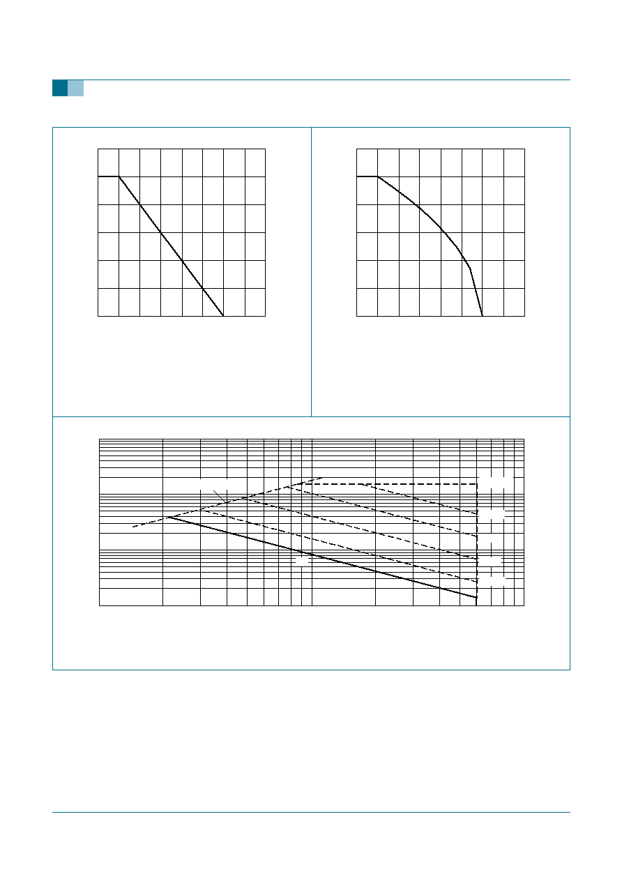
Fig 1.
Normalized total power dissipation as a
function of solder point temperature
Fig 2.
Normalized continuous drain current as a
function of solder point temperature
T
sp
= 25
∞
C; I
DM
is single pulse
Fig 3.
Safe operating area; continuous and peak drain currents as a function of drain-source voltage
03aa17
0
40
80
120
0
50
100
150
200
T
sp
(
∞
C)
P
der
(%)
03aa25
0
40
80
120
0
50
100
150
200
T
sp
(
∞
C)
I
der
(%)
P
der
P
tot
P
tot 25 C
∞
(
)
------------------------
100 %
◊
=
I
der
I
D
I
D 25 C
∞
(
)
---------------------
100 %
◊
=
03ai10
10
-2
10
-1
1
10
1
10
10
2
V
DS
(V)
I
D
(A)
DC
100 ms
10 ms
Limit R
DSon
= V
DS
/ I
D
1 ms
t
p
= 10
µ
s
100
µ
s
9397 750 14944
© Koninklijke Philips Electronics N.V. 2005. All rights reserved.
Product data sheet
Rev. 02 -- 26 April 2005
4 of 11
Philips Semiconductors
2N7002E
N-channel TrenchMOSTM FET
5.
Thermal characteristics
Table 4:
Thermal characteristics
Symbol Parameter
Conditions
Min
Typ
Max
Unit
R
th(j-sp)
thermal resistance from junction to solder point
Figure 4
-
-
150
K/W
R
th(j-a)
thermal resistance from junction to ambient
mounted on a printed-circuit
board; minimum footprint;
vertical in still air
-
-
350
K/W
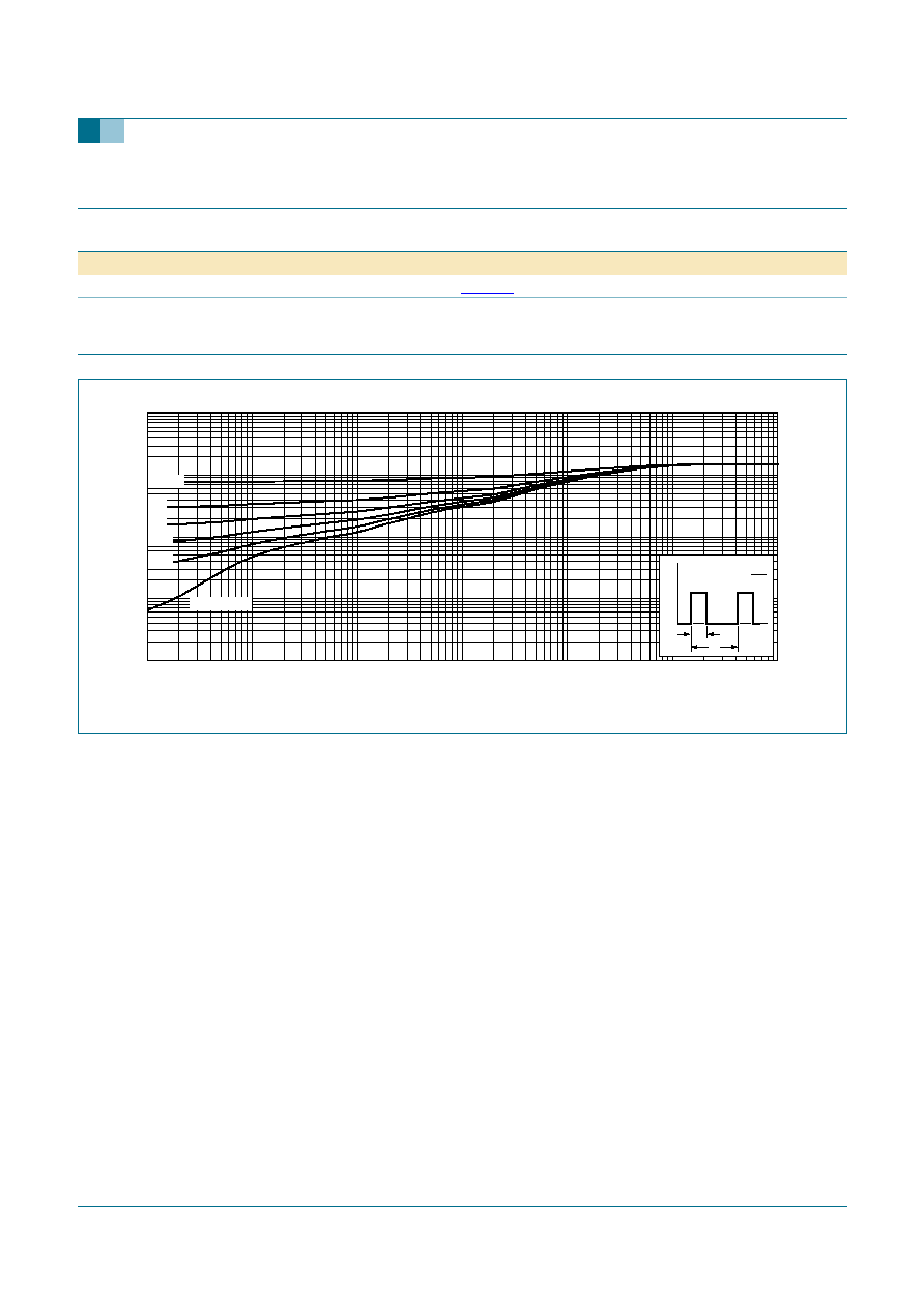
Fig 4.
Transient thermal impedance from junction to solder point as a function of pulse duration
03ai09
10
-1
1
10
10
2
10
3
10
-5
10
-4
10
-3
10
-2
10
-1
1
10
t
p
(s)
Z
th(j-sp)
K/W
single pulse
0.2
0.1
0.05
0.02
= 0.5
t
p
T
P
t
t
p
T
=

9397 750 14944
© Koninklijke Philips Electronics N.V. 2005. All rights reserved.
Product data sheet
Rev. 02 -- 26 April 2005
5 of 11
Philips Semiconductors
2N7002E
N-channel TrenchMOSTM FET
6.
Characteristics
Table 5:
Characteristics
T
j
= 25
∞
C unless otherwise specified.
Symbol Parameter
Conditions
Min
Typ
Max
Unit
Static characteristics
V
(BR)DSS
drain-source breakdown voltage
I
D
= 10
µ
A; V
GS
= 0 V
T
j
= 25
∞
C
60
-
-
V
T
j
=
-
55
∞
C
55
-
-
V
V
GS(th)
gate-source threshold voltage
I
D
= 1 mA; V
DS
= V
GS
;
Figure 9
and
10
T
j
= 25
∞
C
1
2
3
V
T
j
= 150
∞
C
0.6
-
-
V
T
j
=
-
55
∞
C
-
-
3.5
V
I
DSS
drain-source leakage current
V
DS
= 48 V; V
GS
= 0 V
T
j
= 25
∞
C
-
0.01
1
µ
A
T
j
= 150
∞
C
-
-
10
µ
A
I
GSS
gate-source leakage current
V
GS
=
±
15 V; V
DS
= 0 V
-
10
100
nA
R
DSon
drain-source on-state resistance
V
GS
= 10 V; I
D
= 500 mA;
Figure 6
and
8
T
j
= 25
∞
C
-
2.3
3
T
j
= 150
∞
C
-
4.2
5.55
V
GS
= 4.5 V; I
D
= 75 mA;
Figure 6
and
8
-
3.1
4
Dynamic characteristics
g
fs
forward transconductance
V
DS
= 10 V; I
D
= 200 mA
100
300
-
mS
C
iss
input capacitance
V
GS
= 0 V; V
DS
= 10 V; f = 1 MHz;
Figure 11
-
25
40
pF
C
oss
output capacitance
-
18
30
pF
C
rss
reverse transfer capacitance
-
7.5
10
pF
t
on
turn-on delay time
V
DD
= 50 V; R
L
= 250
; V
GS
= 10 V;
R
G
= 50
;
R
GS
= 50
-
3
10
ns
t
off
turn-off delay time
-
12
15
ns
Source-drain diode
V
SD
source-drain (diode forward) voltage
I
S
= 300 mA; V
GS
= 0 V;
Figure 12
-
0.85
1.5
V
t
rr
reverse recovery time
I
S
= 300 mA; dI
S
/dt =
-
100 A/
µ
s;
V
GS
= 0 V
-
30
-
ns
Q
r
recovered charge
-
30
-
nC