
1.
Product profile
1.1 General description
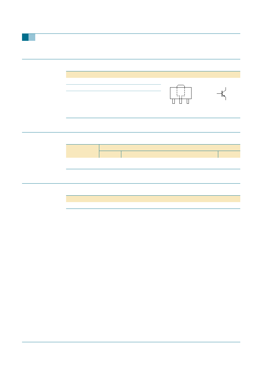
NPN low V
CEsat
Breakthrough in Small Signal (BISS) transistor in a SOT89 (SC-62/
TO-243) SMD plastic package.
PNP complement: 2PB1424.
1.2 Features
s
Low collector-emitter saturation voltage V
CEsat
s
High collector current capability: I
C
and I
CM
s
High collector current gain (h
FE
) at high I
C
s
High efficiency due to less heat generation
s
Smaller required Printed-Circuit Board (PCB) area than for conventional transistors
1.3 Applications
s
DC-to-DC conversion
s
MOSFET gate driving
s
Motor control
s
Charging circuits
s
Power switches (e.g. motors, fans)
s
Thin Film Transistor (TFT) backlight inverter
1.4 Quick reference data
2PD2150
20 V, 3 A NPN low V
CEsat
(BISS) transistor
Rev. 01 -- 22 April 2005
Product data sheet
Table 1:
Quick reference data
Symbol
Parameter
Conditions
Min
Typ
Max
Unit
V
CEO
collector-emitter voltage
open base
-
-
20
V
I
CM
peak collector current
single pulse;
t
p
1 ms
-
-
3
A
h
FE
DC current gain
V
CE
= 2 V;
I
C
= 0.1 A
180
-
390
9397 750 14987
� Koninklijke Philips Electronics N.V. 2005. All rights reserved.
Product data sheet
Rev. 01 -- 22 April 2005
2 of 11
Philips Semiconductors
2PD2150
20 V, 3 A NPN low V
CEsat
(BISS) transistor
2.
Pinning information
3.
Ordering information
4.
Marking
Table 2:
Pinning
Pin
Description
Simplified outline
Symbol
1
emitter
2
collector
3
base
3
2
1
sym042
1
2
3
Table 3:
Ordering information
Type number
Package
Name
Description
Version
2PD2150
SC-62
plastic surface mounted package; collector pad for
good heat transfer; 3 leads
SOT89
Table 4:
Marking codes
Type number
Marking code
2PD2150
M2
9397 750 14987
� Koninklijke Philips Electronics N.V. 2005. All rights reserved.
Product data sheet
Rev. 01 -- 22 April 2005
3 of 11
Philips Semiconductors
2PD2150
20 V, 3 A NPN low V
CEsat
(BISS) transistor
5.
Limiting values
[1]
Device mounted on an FR4 PCB, single-sided copper, tin-plated and standard footprint.
[2]
Device mounted on an FR4 PCB, single-sided copper, tin-plated, mounting pad for collector 1 cm
2
.
[3]
Device mounted on an FR4 PCB, single-sided copper, tin-plated, mounting pad for collector 6 cm
2
.
Table 5:
Limiting values
In accordance with the Absolute Maximum Rating System (IEC 60134).
Symbol
Parameter
Conditions
Min
Max
Unit
V
CBO
collector-base voltage
open emitter
-
40
V
V
CEO
collector-emitter voltage
open base
-
20
V
V
EBO
emitter-base voltage
open collector
-
5
V
I
C
collector current (DC)
-
1
A
I
CM
peak collector current
single pulse;
t
p
1 ms
-
3
A
P
tot
total power dissipation
T
amb
25
�
C
[1]
-
500
mW
[2]
-
850
mW
[3]
-
1200
mW
T
j
junction temperature
-
150
�
C
T
amb
ambient temperature
-
65
+150
�
C
T
stg
storage temperature
-
65
+150
�
C
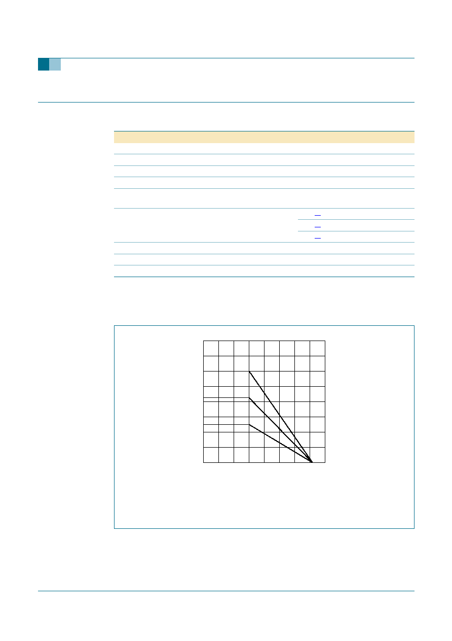
(1) FR4 PCB; mounting pad for collector 6 cm
2
(2) FR4 PCB; mounting pad for collector 1 cm
2
(3) FR4 PCB; standard footprint
Fig 1.
Power derating curves
Tamb (
�
C)
-
65
-
35
175
115
-
5
55
145
25
85
006aaa449
800
400
1200
1600
P
tot
(mW)
0
(1)
(2)
(3)

9397 750 14987
� Koninklijke Philips Electronics N.V. 2005. All rights reserved.
Product data sheet
Rev. 01 -- 22 April 2005
4 of 11
Philips Semiconductors
2PD2150
20 V, 3 A NPN low V
CEsat
(BISS) transistor
6.
Thermal characteristics
[1]
Device mounted on an FR4 PCB, single-sided copper, tin-plated and standard footprint.
[2]
Device mounted on an FR4 PCB, single-sided copper, tin-plated, mounting pad for collector 1 cm
2
.
[3]
Device mounted on an FR4 PCB, single-sided copper, tin-plated, mounting pad for collector 6 m
2
.
Table 6:
Thermal characteristics
Symbol
Parameter
Conditions
Min
Typ
Max
Unit
R
th(j-a)
thermal resistance from
junction to ambient
in free air
[1]
-
-
250
K/W
[2]
-
-
147
K/W
[3]
-
-
104
K/W
R
th(j-sp)
thermal resistance from
junction to solder point
-
-
20
K/W
FR4 PCB; mounting pad for collector 1 cm
2
Fig 2.
Transient thermal impedance from junction to ambient as a function of pulse time; typical values
006aaa450
10
1
10
2
10
3
Z
th(j-a)
(K/W)
10
-
1
10
-
5
10
10
-
2
10
-
4
10
2
10
-
1
t
p
(s)
10
-
3
10
3
1
duty cycle =
1.00
0.20
0.10
0.05
0.00
0.01
0.75
0.50
0.33
0.02

9397 750 14987
� Koninklijke Philips Electronics N.V. 2005. All rights reserved.
Product data sheet
Rev. 01 -- 22 April 2005
5 of 11
Philips Semiconductors
2PD2150
20 V, 3 A NPN low V
CEsat
(BISS) transistor
7.
Characteristics
[1]
Pulse test: t
p
300
�
s;
0.02.
Table 7:
Characteristics
T
amb
= 25
�
C unless otherwise specified.
Symbol
Parameter
Conditions
Min
Typ
Max
Unit
I
CBO
collector-base cut-off
current
V
CB
= 30 V; I
E
= 0 A
-
-
0.1
�
A
V
CB
= 30 V; I
E
= 0 A;
T
j
= 150
�
C
-
-
10
�
A
I
EBO
emitter-base cut-off
current
V
EB
= 5 V; I
C
= 0 A
-
-
0.1
�
A
h
FE
DC current gain
V
CE
= 2 V; I
C
= 0.1 A
180
-
390
V
CEsat
collector-emitter
saturation voltage
I
C
= 2 A; I
B
= 100 mA
-
-
0.5
V
V
BEon
base-emitter turn-on
voltage
V
CE
= 10 V; I
C
= 5 mA
[1]
-
-
0.7
V
V
CE
= 1 V; I
C
= 1 A
[1]
-
-
1
V
f
T
transition frequency
I
C
= 500 mA; V
CE
= 2 V;
f = 100 MHz
-
220
-
MHz
C
c
collector capacitance
V
CB
= 10 V; I
E
= i
e
= 0 A;
f = 1 MHz
-
20
-
pF