ChipFind - документация

Электронный компонент: 4011B

Скачать:  PDF   ZIP
DATA SHEET
Product specification
File under Integrated Circuits, IC04
January 1995
INTEGRATED CIRCUITS
HEF4011B
gates
Quadruple 2-input NAND gate
For a complete data sheet, please also download:
The IC04 LOCMOS HE4000B Logic
Family Specifications HEF, HEC
The IC04 LOCMOS HE4000B Logic
Package Outlines/Information HEF, HEC
January 1995
2
Philips Semiconductors
Product specification
Quadruple 2-input NAND gate
HEF4011B
gates
DESCRIPTION
The HEF4011B provides the positive quadruple 2-input
NAND function. The outputs are fully buffered for highest
noise immunity and pattern insensitivity of output
impedance.
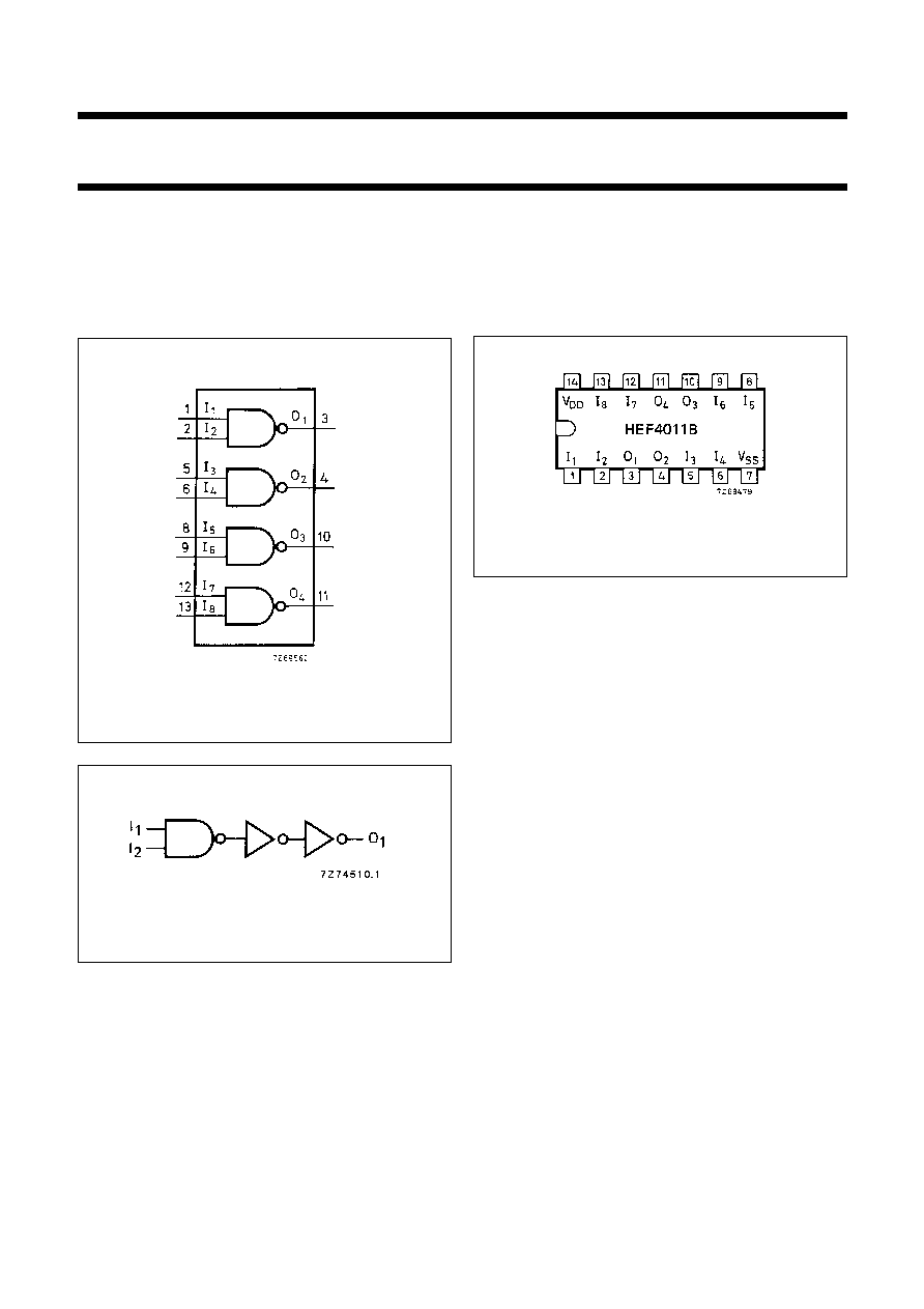
Fig.1 Functional diagram.
HEF4011BP(N):
14-lead DIL; plastic
(SOT27-1)
HEF4011BD(F):
14-lead DIL; ceramic (cerdip)
(SOT73)
HEF4011BT(D):
14-lead SO; plastic
(SOT108-1)
( ): Package Designator North America
Fig.2 Pinning diagram.
FAMILY DATA, I
DD
LIMITS category GATES
See Family Specifications
Fig.3 Logic diagram (one gate).
January 1995
3
Philips Semiconductors
Product specification
Quadruple 2-input NAND gate
HEF4011B
gates
AC CHARACTERISTICS
V
SS
= 0 V; T
amb
= 25
C; C
L
= 50 pF; input transition times
20 ns
V
DD
V
SYMBOL
TYP
MAX
TYPICAL EXTRAPOLATION
FORMULA
Propagation delays
5
55
110
ns
28 ns
+
(0,55 ns/pF) C
L
I
n
O
n
10
t
PHL
; t
PLH
25
45
ns
14 ns
+
(0,23 ns/pF) C
L
15
20
35
ns
12 ns
+
(0,16 ns/pF) C
L
Output transition times
5
60
120
ns
10 ns
+
(1,0 ns/pF) C
L
HIGH to LOW
10
t
THL
30
60
ns
9 ns
+
(0,42 ns/pF) C
L
15
20
40
ns
6 ns
+
(0,28 ns/pF) C
L
5
60
120
ns
10 ns
+
(1,0 ns/pF) C
L
LOW to HIGH
10
t
TLH
30
60
ns
9 ns
+
(0,42 ns/pF) C
L
15
20
40
ns
6 ns
+
(0,28 ns/pF) C
L
V
DD
V
TYPICAL FORMULA FOR P (
W)
Dynamic power
5
1300 f
i
+
(f
o
C
L
)
V
DD
2
where
dissipation per
10
6000 f
i
+
(f
o
C
L
)
V
DD
2
f
i
= input freq. (MHz)
package (P)
15
20 100 f
i
+
(f
o
C
L
)
V
DD
2
f
o
= output freq. (MHz)
C
L
= load capacitance (pF)
(f
o
C
L
) = sum of outputs
V
DD
= supply voltage (V)