
Philips
Semiconductors
74ABT574A
Octal D-type flip-flop (3-State)
Product specification
1995 May 22
INTEGRATED CIRCUITS
IC23 Data Handbook

Philips Semiconductors
Product specification
74ABT574A
Octal D-type flip-flop (3-State)
2
1995 May 22
853-1509 15261
FEATURES
∑
74ABT574A is flow-through pinout version of 74ABT374
∑
Inputs and outputs on opposite side of package allow easy
interface to microprocessors
∑
3-State outputs for bus interfacing
∑
Power-up 3-State
∑
Power-up reset
∑
Common output enable
∑
Latch-up protection exceeds 500mA per Jedec Std 17
∑
ESD protection exceeds 2000 V per MIL STD 883 Method 3015
and 200 V per Machine Model
∑
Live insertion/extraction permitted.
DESCRIPTION
The 74ABT574A high-performance BiCMOS device combines low
static and dynamic power dissipation with high speed and high
output drive.
The 74ABT574A is an 8-bit, edge triggered register coupled to eight
3-State output buffers. The two sections of the device are controlled
independently by the clock (CP) and Output Enable (OE) control
gates. The state of each D input (one set-up time before the
Low-to-High clock transition) is transferred to the corresponding
flip-flop's Q output.
When OE is Low, the stored data appears at the outputs. When OE
is High, the outputs are in the High-impedance "off" state, which
means they will neither drive nor load the bus.
The 3-State output buffers are designed to drive heavily loaded
3-State buses, MOS memories, or MOS microprocessors. The
active-Low Output Enable (OE) controls all eight 3-State buffers
independent of the clock operation.
QUICK REFERENCE DATA
SYMBOL
PARAMETER
CONDITIONS
T
amb
= 25
∞
C; GND = 0V
TYPICAL
UNIT
t
PLH
t
PHL
Propagation delay
CP to Qn
C
L
= 50pF; V
CC
= 5V
3.0
3.4
ns
C
IN
Input capacitance
V
I
= 0V or V
CC
3
pF
C
OUT
Output capacitance
Outputs disabled; V
O
= 0V or V
CC
6
pF
I
CCZ
Total supply current
Outputs disabled; V
CC
=5.5V
100
µ
A
ORDERING INFORMATION
PACKAGES
TEMPERATURE RANGE
OUTSIDE NORTH AMERICA
NORTH AMERICA
DWG NUMBER
20-Pin Plastic DIP
≠40
∞
C to +85
∞
C
74ABT574A N
74ABT574A N
SOT146-1
20-Pin plastic SO
≠40
∞
C to +85
∞
C
74ABT574A D
74ABT574A D
SOT163-1
20-Pin Plastic SSOP Type II
≠40
∞
C to +85
∞
C
74ABT574A DB
74ABT574A DB
SOT339-1
20-Pin Plastic TSSOP Type I
≠40
∞
C to +85
∞
C
74ABT574A PW
7ABT574APW DH
SOT360-1
PIN CONFIGURATION
20
19
18
17
16
15
14
13
12
10
11
9
8
7
6
5
4
3
2
1
OE
D0
D1
D2
D3
D4
D5
D6
D7
GND
V
CC
Q0
Q1
Q2
Q3
Q4
Q5
Q6
Q7
CP
SA00103
PIN DESCRIPTION
PIN
NUMBER
SYMBOL
FUNCTION
1
OE
Output enable input (active-Low)
2, 3, 4, 5,
6, 7, 8, 9
D0-D7
Data inputs
19, 18, 17,
16, 15, 14,
13, 12
Q0-Q7
Data outputs
11
CP
Clock pulse input (active rising edge)
10
GND
Ground (0V)
20
V
CC
Positive supply voltage

Philips Semiconductors
Product specification
74ABT574A
Octal D-type flip-flop (3-State)
1995 May 22
3
LOGIC SYMBOL
11
1
CP
OE
2
3
4
5
6
7
8
9
D0
D1
D2
D3
D4
D5
D6
D7
19
18
17
16
15
14
13
12
Q0
Q1
Q2
Q3
Q4
Q5
Q6
Q7
SA00104
LOGIC SYMBOL (IEEE/IEC)
1
2
19
3
18
4
17
5
16
EN
11
C1
6
15
7
14
8
13
9
12
2D
1
SA00105
FUNCTION TABLE
INPUTS
INTERNAL
OUTPUTS
OPERATING
OE
CP
Dn
INTERNAL
REGISTER
Q0 ≠ Q7
OPERATING
MODE
L
L
l
h
L
H
L
H
Load and read
register
L
X
NC
NC
Hold
H
H
X
Dn
NC
Dn
Z
Z
Disable outputs
H = High voltage level
h
= High voltage level one set-up time prior to the Low≠to≠High
clock transition
L
= Low voltage level
l
= Low voltage level one set-up time prior to the Low≠to≠High
clock transition
NC= No change
X = Don't care
Z = High impedance "off" state
= Low-to-High clock transition
= not a Low-to-High clock transition
LOGIC DIAGRAM
CP Q
D
D0
Q0
CP Q
D
D1
CP Q
D
D2
CP Q
D
D3
CP Q
D
D4
CP Q
D
D5
CP Q
D
D6
CP Q
D
D7
Q1
Q2
Q3
Q4
Q5
Q6
Q7
CP
OE
SA00106
2
3
4
5
6
7
8
9
11
1
19
18
17
16
15
14
13
12

Philips Semiconductors
Product specification
74ABT574A
Octal D-type flip-flop (3-State)
1995 May 22
4
ABSOLUTE MAXIMUM RATINGS
1, 2
SYMBOL
PARAMETER
CONDITIONS
RATING
UNIT
V
CC
DC supply voltage
≠0.5 to +7.0
V
I
IK
DC input diode current
V
I
< 0
≠18
mA
V
I
DC input voltage
3
≠1.2 to +7.0
V
I
OK
DC output diode current
V
O
< 0
≠50
mA
V
OUT
DC output voltage
3
output in Off or High state
≠0.5 to +5.5
V
I
OUT
DC output current
output in Low state
128
mA
T
stg
Storage temperature range
≠65 to 150
∞
C
NOTES:
1. Stresses beyond those listed may cause permanent damage to the device. These are stress ratings only and functional operation of the
device at these or any other conditions beyond those indicated under "recommended operating conditions" is not implied. Exposure to
absolute-maximum-rated conditions for extended periods may affect device reliability.
2. The performance capability of a high-performance integrated circuit in conjunction with its thermal environment can create junction
temperatures which are detrimental to reliability. The maximum junction temperature of this integrated circuit should not exceed 150
∞
C.
3. The input and output voltage ratings may be exceeded if the input and output current ratings are observed.
RECOMMENDED OPERATING CONDITIONS
SYMBOL
PARAMETER
LIMITS
UNIT
SYMBOL
PARAMETER
Min
Max
UNIT
V
CC
DC supply voltage
4.5
5.5
V
V
I
Input voltage
0
V
CC
V
V
IH
High-level input voltage
2.0
V
V
IL
Low-level input voltage
0.8
V
I
OH
High-level output current
≠32
mA
I
OL
Low-level output current
64
mA
t/
v
Input transition rise or fall rate
0
5
ns/V
T
amb
Operating free-air temperature range
≠40
+85
∞
C
Philips Semiconductors
Product specification
74ABT574A
Octal D-type flip-flop (3-State)
1995 May 22
5
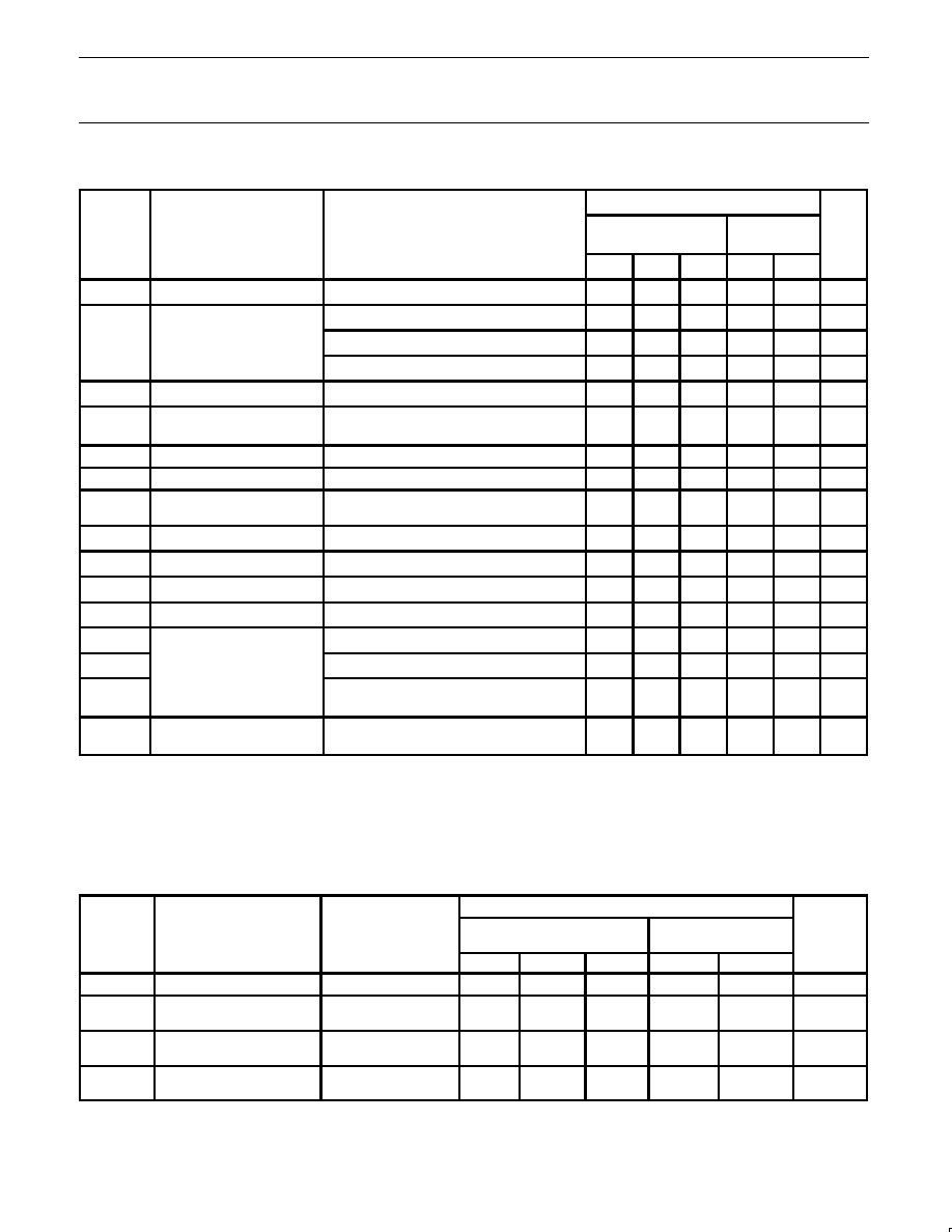
DC ELECTRICAL CHARACTERISTICS
LIMITS
SYMBOL
PARAMETER
TEST CONDITIONS
T
amb
= +25
∞
C
T
amb
= ≠40
∞
C
to +85
∞
C
UNIT
Min
Typ
Max
Min
Max
V
IK
Input clamp voltage
V
CC
= 4.5V; I
IK
= ≠18mA
≠0.9
≠1.2
≠1.2
V
V
CC
= 4.5V; I
OH
= ≠3mA; V
I
= V
IL
or V
IH
2.5
2.9
2.5
V
V
OH
High-level output voltage
V
CC
= 5.0V; I
OH
= ≠3mA; V
I
= V
IL
or V
IH
3.0
3.4
3.0
V
V
CC
= 4.5V; I
OH
= ≠32mA; V
I
= V
IL
or V
IH
2.0
2.4
2.0
V
V
OL
Low-level output voltage
V
CC
= 4.5V; I
OL
= 64mA; V
I
= V
IL
or V
IH
0.42
0.55
0.55
V
V
RST
Power-up output low
voltage
3
V
CC
= 5.5V; I
O
= 1mA; V
I
= GND or V
CC
0.13
0.55
0.55
V
I
I
Input leakage current
V
CC
= 5.5V; V
I
= GND or 5.5V
±
0.01
±
1.0
±
1.0
µ
A
I
OFF
Power-off leakage current
V
CC
= 0.0V; V
O
or V
I
4.5V
±
5.0
±
100
±
100
µ
A
I
PU
/I
PD
Power-up/down 3-State
output current
4
V
CC
= 2.0V; V
O
= 0.5V; V
I
= GND or V
CC;
V
OE
= Don't care
±
5.0
±
50
±
50
µ
A
I
OZH
3-State output High current
V
CC
= 5.5V; V
O
= 2.7V; V
I
= V
IL
or V
IH
5.0
50
50
µ
A
I
OZL
3-State output Low current
V
CC
= 5.5V; V
O
= 0.5V; V
I
= V
IL
or V
IH
≠5.0
≠50
≠50
µ
A
I
CEX
Output High leakage current
V
CC
= 5.5V; V
O
= 5.5V; V
I
= GND or V
CC
5.0
50
50
µ
A
I
O
Output current
1
V
CC
= 5.5V; V
O
= 2.5V
≠40
≠180
≠40
≠180
mA
I
CCH
V
CC
= 5.5V; Outputs High, V
I
= GND or V
CC
100
250
250
µ
A
I
CCL
Quiescent supply current
V
CC
= 5.5V; Outputs Low, V
I
= GND or V
CC
24
30
30
mA
I
CCZ
V
CC
= 5.5V; Outputs 3-State;
V
I
= GND or V
CC
100
250
250
µ
A
I
CC
Additional supply current per
input pin
2
V
CC
= 5.5V; one input at 3.4V,
other inputs at V
CC
or GND
0.5
1.5
1.5
mA
NOTES:
1. Not more than one output should be tested at a time, and the duration of the test should not exceed one second.
2. This is the increase in supply current for each input at 3.4V.
3. For valid test results, data must not be loaded into the flip-flops (or latches) after applying the power.
4. This parameter is valid for any V
CC
between 0V and 2.1V, with a transition time of up to 10 msec. From V
CC
= 2.1V to V
CC
= 5V
"
10% a
transition time of up to 100
µ
sec is permitted.
AC CHARACTERISTICS
GND = 0V, t
R
= t
F
= 2.5ns, C
L
= 50pF, R
L
= 500
LIMITS
SYMBOL
PARAMETER
WAVEFORM
T
amb
= +25
o
C
V
CC
= +5.0V
T
amb
= -40 to +85
o
C
V
CC
= +5.0V
±
0.5V
UNIT
Min
Typ
Min
Min
Max
f
MAX
Maximum clock frequency
1
150
400
150
ns
t
PLH
t
PHL
Propagation delay
CP to Qn
1
1.5
2.0
3.0
3.4
4.4
4.7
1.5
2.0
5.0
5.1
ns
t
PZH
t
PZL
Output enable time
to High and Low level
3
4
1.0
2.5
2.9
3.8
4.1
5.2
1.0
2.5
5.0
5.7
ns
t
PHZ
t
PLZ
Output disable time
from High and Low level
3
4
1.8
1.4
3.1
2.6
4.3
3.8
1.8
1.4
5.0
4.0
ns