Philips Semiconductors
Product specification
74ABT16825A
74ABTH16825A
18-bit buffer/line driver; non-inverting (3-State)
2
1998 Feb 25
853-1804 19018
FEATURES
∑
Multiple V
CC
and GND pins minimize switching noise
∑
Live insertion/extraction permitted
∑
3-State output buffers
∑
Power-up 3-State
∑
74ABTH16825A incorporates bus-hold data inputs which
eliminate the need for external pull-up resistors to hold unused
inputs
∑
Output capability: +64mA/≠32mA
∑
Latch-up protection exceeds 500mA per Jedec Std 17
∑
ESD protection exceeds 2000V per MIL STD 883 Method 3015
and 200V per Machine Model
∑
Bus-hold data inputs eliminate the need for external pull-up
resistors to hold unused inputs
DESCRIPTION
The74ABT16825A high-performance BiCMOS device combines low
static and dynamic power dissipation with high speed and high
output drive.
The74ABT16825A 18-bit buffers provide high performance bus
interface buffering for wide data/address paths or buses carrying
parity. They have NOR Output Enables (nOE1, nOE2) for maximum
control flexibility.
Two options are available, 74ABT16825A which does not have the
bus-hold feature and 74ABTH16825A which incorporates the
bus-hold feature.
QUICK REFERENCE DATA
SYMBOL
PARAMETER
CONDITIONS
T
amb
= 25
∞
C; GND = 0V
TYPICAL
UNIT
t
PLH
t
PHL
Propagation delay
nAx to nYx
C
L
= 50pF; V
CC
= 5V
1.8
1.4
ns
C
IN
Input capacitance
V
I
= 0V or V
CC
4
pF
C
OUT
Output capacitance
V
O
= 0V or V
CC
; 3-State
6
pF
I
CCZ
Quiescent supply current
Outputs disabled; V
CC
= 5.5V
500
µ
A
I
CCL
Quiescent su
ly current
Outputs Low; V
CC
= 5.5V
9
mA
ORDERING INFORMATION
PACKAGES
TEMPERATURE RANGE
OUTSIDE NORTH AMERICA
NORTH AMERICA
DWG NUMBER
56-pin SSOP Type III
≠40
∞
C to +85
∞
C
74ABT16825A DL
BT16825A DL
SOT371-1
56-pin TSSOP Type II
≠40
∞
C to +85
∞
C
74ABT16825A DGG
BT16825A DGG
SOT364-1
56-pin SSOP Type III
≠40
∞
C to +85
∞
C
74ABTH16825A DL
BH16825A DL
SOT371-1
56-pin TSSOP Type II
≠40
∞
C to +85
∞
C
74ABTH16825A DGG
BH16825A DGG
SOT364-1
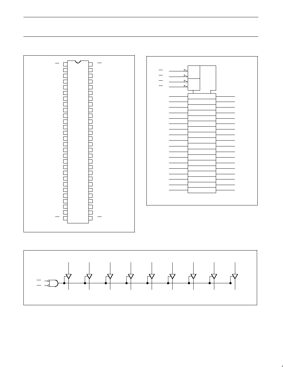
PIN DESCRIPTION
PIN NUMBER
SYMBOL
FUNCTION
55, 54, 52, 51, 49, 48, 47, 45, 44,
41, 40, 38, 37, 36, 34, 33, 31, 30
1A0 ≠ 1A9
2A0 ≠ 2A9
Data inputs
2, 3, 5, 6, 8, 9, 10, 12, 13
16, 17, 19, 20, 21, 23, 24, 26, 27
1Y0 ≠ 1Y9
2Y0 ≠ 2Y9
Data outputs
1, 56
28, 29
1OE0, 1OE1
2OE0, 2OE1
Output enable inputs (active-Low)
4, 11, 14, 15, 18, 25, 32, 39, 42, 43, 46, 53
GND
Ground (0V)
7, 22, 35, 50
V
CC
Positive supply voltage

Philips Semiconductors
Product specification
74ABT16825A
74ABTH16825A
18-bit buffer/line driver; non-inverting (3-State)
1998 Feb 25
4
FUNCTION TABLE
INPUTS
OUTPUTS
OPERATING
nOEx
nAx
nYx
MODE
L
L
L
Transparent
L
H
H
Transparent
H
X
Z
High impedance
H = High voltage level
L
= Low voltage level
X = Don't care
Z = High impedance "off " state
LOGIC SYMBOL
55
54
52
51
49
48
47
45
1A0 1A1
1A2
1A3 1A4
1A5 1A6
1A7
1Y0 1Y1
1Y2
1Y3 1Y4
1Y5 1Y6
1Y7
2
3
5
6
8
9
10
12
1
56
1OE0
1OE1
44
1A8
1Y8
13
41
40
38
37
36
34
33
31
2A0 2A1
2A2
2A3 2A4
2A5 2A6
2A7
2Y0 2Y1
2Y2
2Y3 2Y4
2Y5 2Y6
2Y7
16
17
19
20
21
23
24
26
28
29
2OE0
2OE1
30
2A8
2Y8
27
SA00072
ABSOLUTE MAXIMUM RATINGS
1, 2
SYMBOL
PARAMETER
CONDITIONS
RATING
UNIT
V
CC
DC supply voltage
≠0.5 to +7.0
V
I
IK
DC input diode current
V
I
< 0
≠18
mA
V
I
DC input voltage
3
≠1.2 to +7.0
V
I
OK
DC output diode current
V
O
< 0
≠50
mA
V
OUT
DC output voltage
3
Output in Off or High state
≠0.5 to +5.5
V
I
DC output current
Output in Low state
128
mA
I
OUT
DC output current
Output in High state
≠64
mA
T
stg
Storage temperature range
≠65 to 150
∞
C
NOTES:
1. Stresses beyond those listed may cause permanent damage to the device. These are stress ratings only and functional operation of the
device at these or any other conditions beyond those indicated under "recommended operating conditions" is not implied. Exposure to
absolute-maximum-rated conditions for extended periods may affect device reliability.
2. The performance capability of a high-performance integrated circuit in conjunction with its thermal environment can create junction
temperatures which are detrimental to reliability. The maximum junction temperature of this integrated circuit should not exceed 150
∞
C.
3. The input and output voltage ratings may be exceeded if the input and output current ratings are observed.
RECOMMENDED OPERATING CONDITIONS
SYMBOL
PARAMETER
LIMITS
UNIT
SYMBOL
PARAMETER
MIN
MAX
UNIT
V
CC
DC supply voltage
4.5
5.5
V
V
I
Input voltage
0
V
CC
V
V
IH
High-level input voltage
2.0
V
V
IL
Low-level Input voltage
0.8
V
I
OH
High-level output current
≠32
mA
I
OL
Low-level output current
64
mA
t/
v
Input transition rise or fall rate
0
10
ns/V
T
amb
Operating free-air temperature range
≠40
+85
∞
C
Philips Semiconductors
Product specification
74ABT16825A
74ABTH16825A
18-bit buffer/line driver; non-inverting (3-State)
1998 Feb 25
5
DC ELECTRICAL CHARACTERISTICS
LIMITS
SYMBOL
PARAMETER
TEST CONDITIONS
T
amb
= +25
∞
C
T
amb
= ≠40
∞
C
to +85
∞
C
UNIT
MIN
TYP
MAX
MIN
MAX
V
IK
Input clamp voltage
V
CC
= 4.5V; I
IK
= ≠18mA
≠0.9
≠1.2
≠1.2
V
V
CC
= 4.5V; I
OH
= ≠3mA; V
I
= V
IL
or V
IH
2.5
2.9
2.5
V
V
OH
High-level output voltage
V
CC
= 5.0V; I
OH
= ≠3mA; V
I
= V
IL
or V
IH
3.0
3.4
3.0
V
V
CC
= 4.5V; I
OH
= ≠32mA; V
I
= V
IL
or V
IH
2.0
2.4
2.0
V
V
OL
Low-level output voltage
V
CC
= 4.5V; I
OL
= 64mA; V
I
= V
IL
or V
IH
0.42
0.55
0.55
V
I
I
Input leakage current
ABT16825A
V
CC
= 5.5V; V
I
= GND or 5.5V
±
0.01
±
1.0
±
1.0
µ
A
I
Input leakage current
V
CC
= 5.5V; V
I
= V
CC
or GND
Control
pins
±
0.01
±
1
±
1
µ
A
I
I
In ut leakage current
74ABTH16825A
V
CC
= 5.5V; V
I
= V
CC
Data pins
4
0.01
1
1
µ
A
V
CC
= 5.5V; V
I
= 0
Data ins
4
≠1
≠3
≠5
µ
A
Bus Hold current A inputs
5
V
CC
= 4.5V; V
I
= 0.8V
35
35
I
HOLD
Bus Hold current A inputs
5
74ABTH16825A
V
CC
= 4.5V; V
I
= 2.0V
≠75
≠75
µ
A
74ABTH16825A
V
CC
= 5.5V; V
I
= 0 to 5.5V
±
500
I
OFF
Power-off leakage current
V
CC
= 0.0V; V
O
= 4.5V; V
I
= 0V or 5.5V
±
5.0
±
100
±
100
µ
A
I
PU
/I
PD
Power-up/down 3-State
output current
3
V
CC
= 2.1V; V
O
= 0.5V; V
I
= GND or V
CC
;
V
OE
= Don't care
±
5.0
±
50
±
50
µ
A
I
OZH
3-State output High current
V
CC
= 5.5V; V
O
= 5.5V; V
I
= V
IL
or V
IH
1.0
10
10
µ
A
I
OZL
3-State output Low current
V
CC
= 5.5V; V
O
= 0.0V; V
I
= V
IL
or V
IH
≠1.0
≠10
≠10
µ
A
I
CEX
Output High leakage current
V
CC
= 5.5V; V
O
= 5.5V; V
I
= GND or V
CC
1.0
50
50
µ
A
I
O
Output current
1
V
CC
= 5.5V; V
O
= 2.5V
≠50
≠70
≠180
≠50
≠180
mA
I
CCH
V
CC
= 5.5V; Outputs High, V
I
= GND or V
CC
0.5
1
1
mA
I
CCL
Quiescent supply current
V
CC
= 5.5V; Outputs Low, V
I
= GND or V
CC
9
19
19
mA
I
CCZ
V
CC
= 5.5V; Outputs 3-State;
V
I
= GND or V
CC
0.5
1
1
mA
I
CC
Additional supply current per
input pin
2
74ABT16825A
V
CC
= 5.5V; one input at 3.4V,
other inputs at V
CC
or GND
10
500
500
µ
A
I
CC
Additional supply current per
input pin
2
74ABTH16825A
V
CC
= 5.5V; one input at 3.4V,
other inputs at V
CC
or GND
0.2
1
1
mA
NOTES:
1. Not more than one output should be tested at a time, and the duration of the test should not exceed one second.
2. This is the increase in supply current for each input at 3.4V.
3. This parameter is valid for any V
CC
between 0V and 2.1V with a transition time of up to 10msec. From V
CC
= 2.1V to V
CC
= 5V
±
10% a
transition time of up to 100
µ
sec is permitted.
4. Unused pins at V
CC
or GND.
5. This is the bus hold overdrive current required to force the input to the opposite logic state.
AC CHARACTERISTICS
GND = 0V, t
R
= t
F
= 2.5ns, C
L
= 50pF, R
L
= 500
LIMITS
SYMBOL
PARAMETER
WAVEFORM
T
amb
= +25
o
C
V
CC
= +5.0V
T
amb
= -40 to
+85
o
C
V
CC
= +5.0V
±
0.5V
UNIT
MIN
TYP
MAX
MIN
MAX
t
PLH
t
PHL
Propagation delay
nAx to nYx
1
1.0
0.6
1.8
1.4
2.5
2.0
1.0
0.6
2.8
2.3
ns
t
PZH
t
PZL
Output enable time
to High and Low level
2
1.0
1.0
2.9
2.9
3.8
3.8
1.0
1.0
4.8
5.0
ns
t
PHZ
t
PLZ
Output disable time
from High and Low level
2
2.0
1.6
3.3
2.5
4.5
3.4
2.0
1.6
5.2
3.7
ns