Philips Semiconductors
Product specification
74ALS00A
Quad 2-input NAND gate
2
1991 Feb 08
853≠0038 01670
TYPE
TYPICAL
PROPAGATION DELAY
TYPICAL
SUPPLY CURRENT
(TOTAL)
74ALS00A
4.0ns
1.0mA
ORDERING INFORMATION
ORDER CODE
DESCRIPTION
COMMERCIAL RANGE
V
CC
= 5V
±
10%,
T
amb
= 0
∞
C to +70
∞
C
DRAWING
NUMBER
14-pin plastic DIP
74ALS00AN
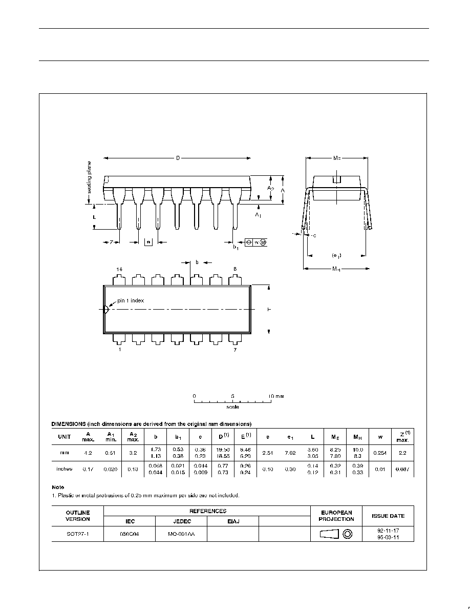
SOT27-1
14-pin plastic SO
74ALS00AD
SOT108-1
14-pin plastic SSOP
Type II
74ALS00ADB
SOT337-1
PIN CONFIGURATION
14
13
12
11
10
9
8
7
6
5
4
3
2
1
1A
1B
1Y
2A
2B
2Y
GND
3Y
3A
3B
4Y
4A
4B
V
CC
SC00001
INPUT AND OUTPUT LOADING AND FAN-OUT TABLE
PINS
DESCRIPTION
74ALS (U.L.)
HIGH/LOW
LOAD VALUE
HIGH/LOW
nA, nB
Data inputs
1.0/1.0
20
µ
A/0.1mA
nY
Data output
20/80
0.4mA/8mA
NOTE:
One (1.0) ALS unit load is defined as: 20
µ
A in the High state and 0.1mA in the Low state.
LOGIC SYMBOL
V
CC
= Pin 14
GND = Pin 7
1
2
4
5
9
10
12
13
1A 1B 2A 2B 3A 3B 4A 4B
1Y 2Y 3Y 4Y
3
6
8
11
SC00002
IEC/IEEE SYMBOL
1
2
4
5
9
10
12
13
&
3
6
8
11
SF00004
LOGIC DIAGRAM
V
CC
= Pin 14
GND = Pin 7
1A
1B
2A
2B
3A
3B
4A
4B
1Y
2Y
3Y
4Y
3
6
8
11
1
2
4
5
9
10
12
13
SC00003
FUNCTION TABLE
INPUTS
OUTPUT
nA
nB
nY
H
H
L
L
X
H
X
L
H
H = High voltage level
L
= Low voltage level
X = Don't care

Philips Semiconductors
Product specification
74ALS00A
Quad 2-input NAND gate
1991 Feb 08
3
ABSOLUTE MAXIMUM RATINGS
(Operation beyond the limit set forth in this table may impair the useful life of the device.
Unless otherwise noted these limits are over the operating free-air temperature range.)
SYMBOL
PARAMETER
RATING
UNIT
V
CC
Supply voltage
≠0.5 to +7.0
V
V
IN
Input voltage
≠0.5 to +7.0
V
I
IN
Input current
≠30 to +5
mA
V
OUT
Voltage applied to output in High output state
≠0.5 to V
CC
V
I
OUT
Current applied to output in Low output state
16
mA
T
amb
Operating free air temperature range
0 to +70
∞
C
T
stg
Storage temperature range
≠65 to +150
∞
C
RECOMMENDED OPERATING CONDITIONS
SYMBOL
PARAMETER
LIMITS
UNIT
MIN
NOM
MAX
V
CC
Supply voltage
4.5
5.0
5.5
V
V
IH
High-level input voltage
2.0
V
V
IL
Low-level input voltage
0.8
V
I
Ik
Input clamp current
≠18
mA
I
OH
High-level output current
≠0.4
mA
I
OL
Low-level output current
8
mA
T
amb
Operating free-air temperature range
0
+70
∞
C
DC ELECTRICAL CHARACTERISTICS
(Over recommended operating free-air temperature range unless otherwise noted.)
SYMBOL
PARAMETER
TEST CONDITIONS
1
LIMITS
UNIT
SYMBOL
PARAMETER
TEST CONDITIONS
1
MIN
TYP
2
MAX
UNIT
V
OH
High-level output voltage
V
CC
±
10%, V
IL
= MAX, V
IH
= MIN, I
OH
= ≠0.4mA
V
CC
≠ 2
V
V
O
Low level output voltage
V
CC
= MIN, V
IL
= MAX,
I
OL
= 4mA
0.25
0.40
V
V
OL
Low-level output voltage
CC
,
IL
,
V
IH
= MIN
I
OL
= 8mA
0.35
0.50
V
V
IK
Input clamp voltage
V
CC
= MIN, I
I
= I
IK
-0.73
-1.5
V
I
I
Input current at maximum input voltage
V
CC
= MAX, V
I
= 7.0V
0.1
mA
I
IH
High-level input current
V
CC
= MAX, V
I
= 2.7V
20
µ
A
I
IL
Low-level input current
V
CC
= MAX, V
I
= 0.5V
-0.1
mA
I
O
Output current
3
V
CC
= MAX, V
O
= 2.25V
-30
-112
mA
I
CC
Supply current (total)
I
CCH
V
CC
= MAX
V
I
= GND
0.5
0.85
mA
I
CC
Supply current (total)
I
CCL
V
CC
= MAX
V
I
= 4.5V
1.5
3.0
mA
NOTES:
1. For conditions shown as MIN or MAX, use the appropriate value specified under recommended operating conditions for the applicable type.
2. All typical values are at V
CC
= 5V, T
amb
= 25
∞
C.
3. The output conditions have been chosen to produce a current that closely approximate one half of the true short-circuit output current, I
OS
.

Philips Semiconductors
Product specification
74ALS00A
Quad 2-input NAND gate
1991 Feb 08
4
AC ELECTRICAL CHARACTERISTICS
LIMITS
SYMBOL
PARAMETER
TEST CONDITION
T
amb
= 0
∞
C to +70
∞
C
V
CC
= +5.0V
±
10%
C
L
= 50pF, R
L
= 500
UNIT
MIN
MAX
t
PLH
t
PHL
Propagation delay
nA, nB to nY
Waveform 1
2.0
2.0
11.0
8.0
ns
AC WAVEFORMS
For all waveforms, V
M
= 1.3V.
V
M
V
M
V
M
V
M
t
PLH
t
PHL
nA, nB
nY
SC00004
Waveform 1.
Propagation Delay for Data to Output
TEST CIRCUIT AND WAVEFORMS
tw
90%
VM
10%
90%
VM
10%
90%
VM
10%
90%
VM
10%
NEGATIVE
PULSE
POSITIVE
PULSE
tw
AMP (V)
0.3V
0.3V
tTHL (tf
f
)
INPUT PULSE REQUIREMENTS
Rep.Rate
t
w
t
TLH
t
THL
1MHz
500ns
2.0ns
2.0ns
Input Pulse Definition
VCC
Family
74ALS
D.U.T.
PULSE
GENERATOR
RL
CL
RT
VIN
VOUT
Test Circuit for Totem-pole Outputs
DEFINITIONS:
R
L
= Load resistor;
see AC electrical characteristics for value.
C
L
= Load capacitance includes jig and probe capacitance;
see AC electrical characteristics for value.
R
T
= Termination resistance should be equal to Z
OUT
of
pulse generators.
tTHL (tf
)
tTLH (tr
)
tTLH (tr
)
AMP (V)
Amplitude
3.5V
1.3V
V
M
SC00005