
Philips
Semiconductors
74ALS573B/74ALS574A
Latch flip≠flop
Product specification
IC05 Data Handbook
1991 Feb 08
INTEGRATED CIRCUITS

Philips Semiconductors
Product specification
74ALS573B/74ALS574A
Latch/flip-flop
74ALS573B
Octal transparent latch (3-State)
74ALS574A
Octal D flip-flop (3-State)
2
1991 Feb 08
853≠1307 01670
FEATURES
∑
74ALS573B is broadside pinout version of 74ALS373
∑
74ALS574A is broadside pinout version of 74ALS374
∑
Inputs and outputs on opposite side of package allow easy
interface to microprocessors
∑
Useful as an input or output port for microprocessors
∑
3-State outputs for bus interfacing
∑
Common output enable
∑
74ALS563A and 74ALS564A are inverting version of 74ALS573B
and 74ALS574A respectively
DESCRIPTION
The 74ALS573B is an octal transparent latch coupled to eight
3-State output devices. The two sections of the device are controlled
independently by enable (E) and output enable (OE) control gates.
The 74ALS573B is functionally identical to the 74ALS373 but has a
broadside pinout configuration to facilitate PC board layout and
allow easy interface with microprocessors.
The data on the D inputs is transferred to the latch outputs when the
enable (E) input is High. The latch remains transparent to the data
input while E is High, and stores the data that is present one setup
time before the High-to-Low enable transition.
The 74ALS574A is functionally identical to the 74ALS374 but has a
broadside pinout configuration to facilitate PC board layout and
allow easy interface with microprocessors.
It is an 8-bit edge triggered register coupled to eight 3-State output
buffers. The two sections of the device are controlled independently
by clock (CP) and output enable (OE) control gates.
The register is fully edge triggered. The state of the D input, one
setup time before the Low-to-High clock transition is transferred to
the corresponding flip-flop's Q output.
The active-Low output enable (OE) controls all eight 3-State buffers
independent of the latch operation. When OE is Low, latched or
transparent data appears at the output.
When OE is High, the outputs are in high impedance "off" state,
which means they will neither drive nor load the bus.
TYPE
TYPICAL
PROPAGATION
DELAY
TYPICAL
SUPPLY CURRENT
(TOTAL)
74ALS573B
5.0ns
12mA
74ALS574A
6.0ns
15mA
ORDERING INFORMATION
ORDER CODE
DESCRIPTION
COMMERCIAL RANGE
V
CC
= 5V
±
10%,
T
amb
= 0
∞
C to +70
∞
C
DRAWING
NUMBER
20-pin plastic DIP
74ALS573BN, 74ALS574AN
SOT146-1
20-pin plastic SOL
74ALS573BD, 74ALS574AD
SOT163-1
20-pin plastic SSOP
Type II
74ALS573BDB,
74ALS574ADB
SOT339-1
INPUT AND OUTPUT LOADING AND FAN-OUT TABLE
PINS
DESCRIPTION
74ALS (U.L.)
HIGH/LOW
LOAD VALUE
HIGH/LOW
D0 ≠ D7
Data inputs
1.0/1.0
20
µ
A/0.2mA
E (74ALS573B)
Latch enable input
1.0/1.0
20
µ
A/0.1mA
OE
Output Enable input (active-Low)
1.0/1.0
20
µ
A/0.1mA
CP (74ALS574A)
Clock pulse input (active rising edge)
1.0/2.0
20
µ
A/0.2mA
Q0 ≠ Q7
Data outputs
130/240
2.6mA/24mA
NOTE:
One (1.0) ALS unit load is defined as: 20
µ
A in the High state and 0.1mA in the Low state.

Philips Semiconductors
Product specification
74ALS573B/74ALS574A
Latch/flip-flop
1991 Feb 08
3
PIN CONFIGURATION ≠ 74ALS573B
1
2
3
4
5
6
7
8
9
10
11
12
13
14
15
16
17
18
19
20
OE
GND
V
CC
E
SF01073
Q0
D0
D1
Q1
D2
Q2
Q3
D3
Q4
D4
Q5
D5
Q6
D6
Q7
D7
PIN CONFIGURATION ≠ 74ALS574A
1
2
3
4
5
6
7
8
9
10
11
12
13
14
15
16
17
18
19
20
OE
GND
V
CC
CP
SF01074
Q0
D0
D1
Q1
D2
Q2
Q3
D3
Q4
D4
Q5
D5
Q6
D6
Q7
D7
LOGIC SYMBOL ≠ 74ALS573B
3
4
5
6
7
8
14
15
16
17
18
19
1
11
E
OE
Q0
D0
D1
Q1
D2
Q2
Q3
D3
Q4
D4
Q5
D5
9
2
12
13
Q6
D6
Q7
D7
SF01075
V
CC
=Pin 20
GND=Pin 10
LOGIC SYMBOL ≠ 74ALS574A
3
4
5
6
7
8
14
15
16
17
18
19
1
11
CP
OE
Q0
D0
D1
Q1
D2
Q2
Q3
D3
Q4
D4
Q5
D5
9
2
12
13
Q6
D6
Q7
D7
SF01076
V
CC
=Pin 20
GND=Pin 10
IEC/IEEE SYMBOL ≠ 74ALS573B
2D
1
SF01077
1
11
2
3
4
5
6
7
8
9
EN1
EN2
19
18
17
16
15
14
13
12
IEC/IEEE SYMBOL ≠ 74ALS574A
2D
1
SF01078
1
11
EN1
C2
2
3
4
5
6
7
8
9
19
18
17
16
15
14
13
12

Philips Semiconductors
Product specification
74ALS573B/74ALS574A
Latch/flip-flop
1991 Feb 08
4
LOGIC DIAGRAM ≠ 74ALS573B
V
CC
= Pin 20
GND = Pin 10
D0
D
E
Q
Q0
2
19
D1
D
E
Q
Q1
3
18
D2
D
E
Q
Q2
4
17
D3
D
E
Q
Q3
5
16
D4
D
E
Q
Q4
6
15
D5
D
E
Q
Q5
7
14
D6
D
E
Q
Q6
8
13
D7
D
E
Q
Q7
9
12
11
E
SC00109
1
OE
FUNCTION TABLE ≠ 74ALS573B
INPUTS
OUTPUTS
INTERNAL
OPERATING MODE
OE
E
Dn
REGISTER
Q0 ≠ Q7
OPERATING MODE
L
H
L
L
L
Enable and read register
L
H
H
H
H
Enable and read register
L
l
L
L
Latch and read register
L
h
H
H
Latch and read register
L
L
X
NC
NC
Hold
H
L
X
NC
Z
Disable outputs
H
H
Dn
Dn
Z
Disable outputs
H = High-voltage level
h
= High state must be present one setup time before the High-to-Low enable transition
L
= Low-voltage level
l
= Low state must be present one setup time before the High-to-Low enable transition
NC= No change
X = Don't care
Z = High impedance "off" state
= High-to-Low enable transition
LOGIC DIAGRAM ≠ 74ALS574A
VCC =
Pin 20
D0
D
CP Q
Q0
2
19
D1
D
CP Q
Q1
3
18
D2
D
CP Q
Q2
4
17
D3
D
CP Q
Q3
5
16
D4
D
CP Q
Q4
6
15
D5
D
CP Q
Q5
7
14
D6
D
CP Q
Q6
8
13
D7
D
CP Q
Q7
9
12
11
OE
CP
GND = Pin 10
SC00110
1

Philips Semiconductors
Product specification
74ALS573B/74ALS574A
Latch/flip-flop
1991 Feb 08
5
FUNCTION TABLE ≠ 74ALS574A
INPUTS
OUTPUTS
INTERNAL
OPERATING MODE
OE
CP
Dn
REGISTER
Q0 ≠ Q7
OPERATING MODE
L
l
L
L
Latch and read register
L
h
H
H
Latch and read register
L
X
NC
NC
Hold
H
X
NC
Z
Disable outputs
H
Dn
Dn
Z
Disable outputs
H = High-voltage level
h
= High state must be present one setup time before the Low-to-High clock transition
L
= Low-voltage level
l
= Low state must be present one setup time before the Low-to-High clock transition
NC= No change
X = Don't care
Z = High impedance "off" state
= Low-to-High clock transition
= Not Low-to-High clock transition
ABSOLUTE MAXIMUM RATINGS
(Operation beyond the limit set forth in this table may impair the useful life of the device.
Unless otherwise noted these limits are over the operating free-air temperature range.)
SYMBOL
PARAMETER
RATING
UNIT
V
CC
Supply voltage
≠0.5 to +7.0
V
V
IN
Input voltage
≠0.5 to +7.0
V
I
IN
Input current
≠30 to +5
mA
V
OUT
Voltage applied to output in High output state
≠0.5 to V
CC
V
I
OUT
Current applied to output in Low output state
48
mA
T
amb
Operating free-air temperature range
0 to +70
∞
C
T
stg
Storage temperature range
≠65 to +150
∞
C
RECOMMENDED OPERATING CONDITIONS
SYMBOL
PARAMETER
LIMITS
UNIT
SYMBOL
PARAMETER
MIN
NOM
MAX
UNIT
V
CC
Supply voltage
4.5
5.0
5.5
V
V
IH
High-level input voltage
2.0
V
V
IL
Low-level input voltage
0.8
V
I
IK
Input clamp current
≠18
mA
I
OH
High-level output current
≠2.6
mA
I
OL
Low-level output current
24
mA
T
amb
Operating free-air temperature range
0
+70
∞
C

Philips Semiconductors
Product specification
74ALS573B/74ALS574A
Latch/flip-flop
1991 Feb 08
6
DC ELECTRICAL CHARACTERISTICS
(Over recommended operating free-air temperature range unless otherwise noted.)
SYMBOL
PARAMETER
TEST CONDITIONS
1
LIMITS
UNIT
SYMBOL
PARAMETER
TEST CONDITIONS
1
MIN
TYP
2
MAX
UNIT
V
O
High level output voltage
V
CC
=
±
10%, V
IL
= MAX,
I
OH
= ≠0.4mA
V
CC
≠ 2
V
V
OH
High-level output voltage
CC
,
IL
,
V
IH
= MIN
I
OH
= MAX
2.4
3.2
V
V
O
Low level output voltage
V
CC
= MIN, V
IL
= MAX,
I
OL
= 12mA
0.25
0.40
V
V
OL
Low-level output voltage
CC
,
IL
,
V
IH
= MIN
I
OL
= 24mA
0.35
0.50
V
V
IK
Input clamp voltage
V
CC
= MIN, I
I
= I
IK
≠0.73
≠1.2
V
I
I
Input current at minimum input voltage
V
CC
= MAX, V
I
= 7.0V
0.1
mA
I
IH
High-level input current
V
CC
= MAX, V
I
= 2.7V
20
µ
A
I
Low level input current
74ALS573B
V
CC
= MAX, V
I
= 0.4V
≠0.1
mA
I
IL
Low-level input current
74ALS574A
V
CC
= MAX, V
I
= 0.4V
≠0.2
mA
I
OZH
Off-state output current,
High-level voltage applied
V
CC
= MAX, V
I
= 2.7V
20
µ
A
I
OZL
Off-state output current,
Low-level voltage applied
V
CC
= MAX, V
I
= 0.4V
≠20
µ
A
I
O
Output current
3
V
CC
= MAX, V
O
= 2.25V
≠30
≠112
mA
I
CCH
7
12
mA
74ALS573B
I
CCL
V
CC
= MAX
13
21
mA
I
CC
Supply current (total)
I
CCZ
15
24
mA
I
CC
Supply current (total)
I
CCH
10
16
mA
74ALS574A
I
CCL
V
CC
= MAX
17
27
mA
I
CCZ
18
28
mA
NOTES:
1. For conditions shown as MIN or MAX, use the appropriate value specified under recommended operating conditions for the applicable type.
2. All typical values are at V
CC
= 5V, T
amb
= 25
∞
C.
3. The output conditions have been chosen to produce a current that closely approximates one half of the true short-circuit output current, I
OS
.

Philips Semiconductors
Product specification
74ALS573B/74ALS574A
Latch/flip-flop
1991 Feb 08
7
AC ELECTRICAL CHARACTERISTICS
LIMITS
SYMBOL
PARAMETER
TEST CONDITION
T
amb
= 0
∞
C to +70
∞
C
V
CC
= +5.0V
±
10%
C
L
= 50pF, R
L
= 500
UNIT
MIN
MAX
t
PLH
t
PHL
Propagation delay
Dn to Qn
Waveform 3
2.0
2.0
10.0
10.0
ns
t
PLH
t
PHL
Propagation delay
E to Qn
74ALS573B
Waveform 2
4.0
4.0
12.0
12.0
ns
t
PZH
t
PZL
Output enable time
to High or Low level
74ALS573B
Waveform 6
Waveform 7
2.0
4.0
9.0
11.0
ns
t
PHZ
t
PLZ
Output disable time
from High or Low level
Waveform 6
Waveform 7
1.0
2.0
9.0
11.0
ns
f
MAX
Maximum clock frequency
Waveform 1
45
MHz
t
PLH
t
PHL
Propagation delay
CP to Qn
Waveform 1
3.0
4.0
12.0
12.0
ns
t
PZH
t
PZL
Output enable time
to High or Low level
74ALS574A
Waveform 6
Waveform 7
2.0
4.0
9.0
11.0
ns
t
PHZ
t
PLZ
Output disable time
from High or Low level
Waveform 6
Waveform 7
1.0
2.0
9.0
11.0
ns
AC SETUP CHARACTERISTICS
LIMITS
SYMBOL
PARAMETER
TEST CONDITION
T
amb
= 0
∞
C to +70
∞
C
V
CC
= +5.0V
±
10%
C
L
= 50pF, R
L
= 500
UNIT
MIN
MAX
t
su
(H)
t
su
(L)
Setup time, High or Low
Dn to E
Waveform 4
6.0
6.0
ns
t
h
(H)
t
h
(L)
Hold time, High or Low
Dn to E
74ALS573B
Waveform 4
6.0
6.0
ns
t
w
(H)
E Pulse width, High
Waveform 1
10.0
ns
t
su
(H)
t
su
(L)
Setup time, High or Low
Dn to CP
Waveform 5
6.0
6.0
ns
t
h
(H)
t
h
(L)
Hold time, High or Low
Dn to CP
74ALS574A
Waveform 5
1.0
1.0
ns
t
w
(H)
t
w
(L)
CP Pulse width,
High or Low
Waveform 5
8.0
12.0
ns

Philips Semiconductors
Product specification
74ALS573B/74ALS574A
Latch/flip-flop
1991 Feb 08
8
AC WAVEFORMS
For all waveforms, V
M
= 1.3V.
The shaded areas indicate when the input is permitted to change for predictable output performance.
CP VM
VM
VM
tw(H)
1/fmax
VM
VM
tPHL
tw(L)
tPLH
Qn
SF00258
Waveform 1.
Propagation Delay for Clock Input to Output,
Clock Pulse Widths, and Maximum Clock Frequency
tPHL
E
VM
VM
VM
tw(H)
VM
VM
Qn
tPLH
SF00259
Waveform 2.
Propagation Delay for Enable to Output and
Enable Pulse Width
Dn
VM
VM
VM
VM
tPHL
tPLH
Qn
SF00260
Waveform 3.
Propagation Delay for Data to Output
VM
VM
VM
VM
VM
VM
tsu(L)
th(L)
tsu(H)
th(H)
E
Dn
SF00261
Waveform 4.
Data Setup Time and Hold Times
VM
VM
VM
VM
VM
VM
tsu(L)
th(L)
tsu(H)
th(H)
CP
Dn
SF00262
Waveform 5.
Data Setup Time and Hold Times
V
M
V
M
V
M
t
PHZ
t
PZH
OE
Qn
V
OH
-0.3V
0V
SC00099
Waveform 6.
3-State Output Enable Time to High Level and
Output Disable Time from High Level
V
M
V
M
V
M
t
PLZ
t
PZL
OE
Qn
V
OL
+0.3V
SC00100
3.5V
Waveform 7.
3-State Output Enable Time to Low Level and
Output Disable Time from Low Level

Philips Semiconductors
Product specification
74ALS573B/74ALS574A
Latch/flip-flop
1991 Feb 08
9
TEST CIRCUIT AND WAVEFORMS
tw
90%
VM
10%
90%
VM
10%
90%
VM
10%
90%
VM
10%
NEGATIVE
PULSE
POSITIVE
PULSE
tw
AMP (V)
0.3V
0.3V
tTHL (tf
f
)
INPUT PULSE REQUIREMENTS
Rep.Rate
t
w
t
TLH
t
THL
1MHz
500ns
2.0ns
2.0ns
Input Pulse Definition
VCC
Family
74ALS
D.U.T.
PULSE
GENERATOR
RL
CL
RT
VIN
VOUT
Test Circuit for 3-State Outputs
DEFINITIONS:
R
L
= Load resistor;
see AC electrical characteristics for value.
C
L
= Load capacitance includes jig and probe capacitance;
see AC electrical characteristics for value.
R
T
= Termination resistance should be equal to Z
OUT
of
pulse generators.
tTHL (tf
)
tTLH (tr
)
tTLH (tr
)
AMP (V)
Amplitude
3.5V
1.3V
V
M
SC00072
RL
7.0V
SWITCH POSITION
TEST
SWITCH
t
PLZ
, t
PZL
closed
All other
open
Philips Semiconductors
Product specification
74ALS573B/74ALS574A
Latch/flip≠flop
1991 Feb 08
10
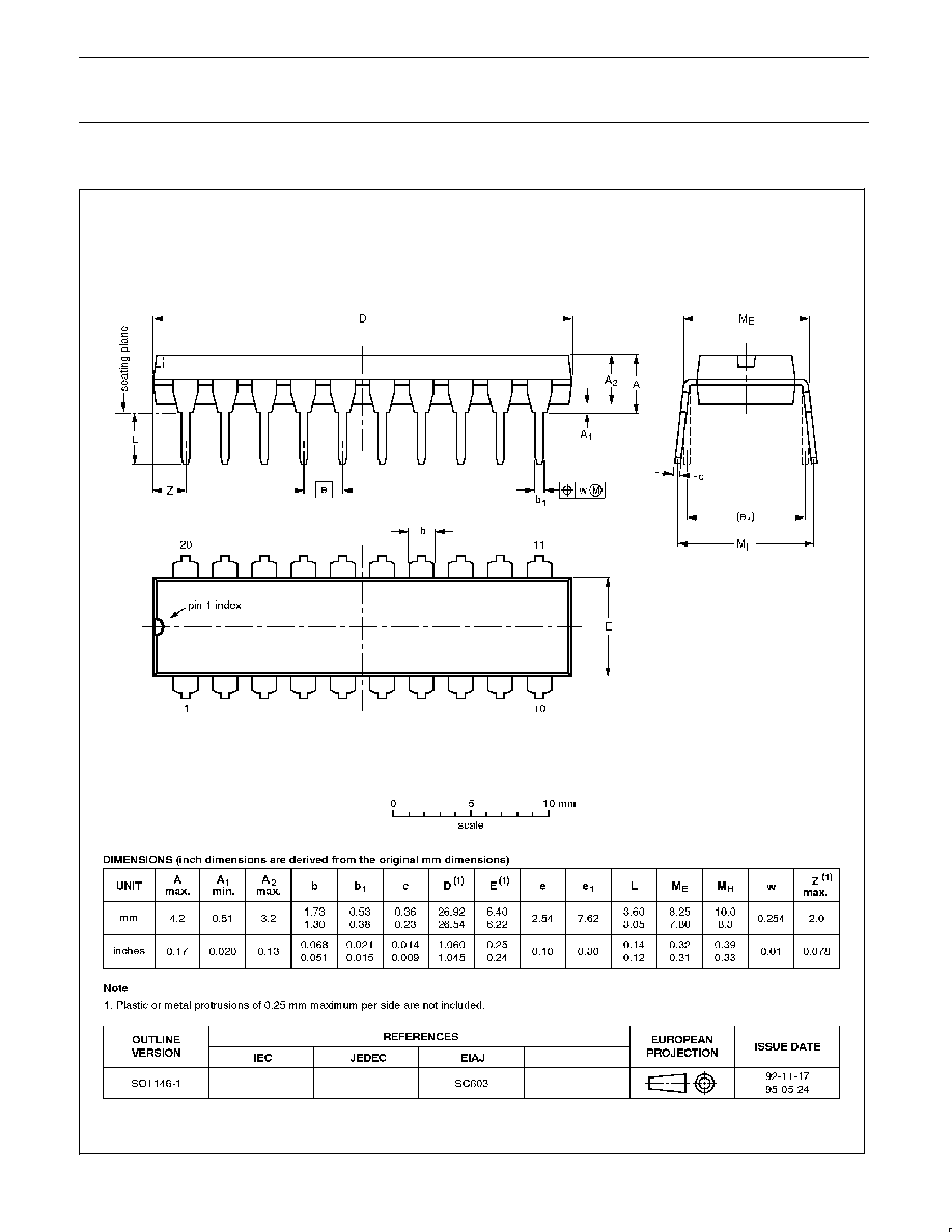
DIP20:
plastic dual in-line package; 20 leads (300 mil)
SOT146-1

Philips Semiconductors
Product specification
74ALS573B/74ALS574A
Latch/flip≠flop
1991 Feb 08
11
SO20:
plastic small outline package; 20 leads; body width 7.5 mm
SOT163-1

Philips Semiconductors
Product specification
74ALS573B/74ALS574A
Latch/flip≠flop
1991 Feb 08
12
SSOP20:
plastic shrink small outline package; 20 leads; body width 5.3 mm
SOT339-1

Philips Semiconductors
Product specification
74ALS573B/74ALS574A
Latch/flip≠flop
1991 Feb 08
13
Philips Semiconductors and Philips Electronics North America Corporation reserve the right to make changes, without notice, in the products,
including circuits, standard cells, and/or software, described or contained herein in order to improve design and/or performance. Philips
Semiconductors assumes no responsibility or liability for the use of any of these products, conveys no license or title under any patent, copyright,
or mask work right to these products, and makes no representations or warranties that these products are free from patent, copyright, or mask
work right infringement, unless otherwise specified. Applications that are described herein for any of these products are for illustrative purposes
only. Philips Semiconductors makes no representation or warranty that such applications will be suitable for the specified use without further testing
or modification.
LIFE SUPPORT APPLICATIONS
Philips Semiconductors and Philips Electronics North America Corporation Products are not designed for use in life support appliances, devices,
or systems where malfunction of a Philips Semiconductors and Philips Electronics North America Corporation Product can reasonably be expected
to result in a personal injury. Philips Semiconductors and Philips Electronics North America Corporation customers using or selling Philips
Semiconductors and Philips Electronics North America Corporation Products for use in such applications do so at their own risk and agree to fully
indemnify Philips Semiconductors and Philips Electronics North America Corporation for any damages resulting from such improper use or sale.
This data sheet contains preliminary data, and supplementary data will be published at a later date. Philips
Semiconductors reserves the right to make changes at any time without notice in order to improve design
and supply the best possible product.
Philips Semiconductors
811 East Arques Avenue
P.O. Box 3409
Sunnyvale, California 94088≠3409
Telephone 800-234-7381
DEFINITIONS
Data Sheet Identification
Product Status
Definition
Objective Specification
Preliminary Specification
Product Specification
Formative or in Design
Preproduction Product
Full Production
This data sheet contains the design target or goal specifications for product development. Specifications
may change in any manner without notice.
This data sheet contains Final Specifications. Philips Semiconductors reserves the right to make changes
at any time without notice, in order to improve design and supply the best possible product.
©
Copyright Philips Electronics North America Corporation 1997
All rights reserved. Printed in U.S.A.
Philips
Semiconductors