
Philips
Semiconductors
74ALS651/74ALS651≠1
74ALS652/74ALS652≠1
Transceiver/register
Product specification
IC05 Data Handbook
1991 Feb 08
INTEGRATED CIRCUITS

Philips Semiconductors
Product specification
74ALS651/74ALS651-1
74ALS652/74ALS652-1
Transceiver/register
74ALS651/651-1
Octal transceiver/register, inverting (3-State)
74ALS652/652-1
Octal transceiver/register, non-inverting (3-State)
2
1991 Feb 08
853≠1407 01670
FEATURES
∑
Independent registers for A and B buses
∑
Multiplexed real-time and stored data
∑
Choice of non-inverting and inverting data paths
∑
3-State outputs
∑
The -1 versions sinks 48mA I
OL
within the
±
5% V
CC
range
DESCRIPTION
The 74LAS651 and 74ALS652 transceivers/registers consist of bus
transceiver circuits with 3-State outputs, D-type flip-flops, and
control circuitry arranged for multiplexed transmission of data
directly from the input bus or the internal registers. Data on the A or
B bus will be clocked into the registers as the appropriate clock pin
goes High. Output enable (OEAB, OEBA) and select (SAB, SBA)
pins are provided for bus management. The 74LAS651-1 and
74ALS652-1 will sink 48mA if the V
CC
is limited to 5.0V
±
0.25V.
TYPE
TYPICAL
f
MAX
TYPICAL
SUPPLY CURRENT
(TOTAL)
74ALS651/74ALS651-1
140MHz
40mA
74ALS652/74ALS652-1
140MHz
46mA
ORDERING INFORMATION
ORDER CODE
DESCRIPTION
COMMERCIAL RANGE
V
CC
= 5V
±
10%,
T
amb
= 0
∞
C to +70
∞
C
DRAWING
NUMBER
24-pin plastic DIP
74ALS651N, 74ALS651-1N,
74ALS652N, 74ALS652-1N
SOT222-1
24-pin plastic SOL
74ALS651D, 74ALS651-1D,
74ALS652D, 74ALS652-1D
SOT137-1
INPUT AND OUTPUT LOADING AND FAN-OUT TABLE
PINS
DESCRIPTION
74ALS (U.L.)
HIGH/LOW
LOAD VALUE
HIGH/LOW
A0 ≠ A7
A inputs
1.0/1.0
70
µ
A/0.1mA
B0 ≠ B7
B inputs
1.0/1.0
70
µ
A/0.1mA
CPAB
A-to-B clock input
1.0/1.0
20
µ
A/0.1mA
CPBA
B-to-A clock input
1.0/1.0
20
µ
A/0.1mA
SAB
A-to-B select input
1.0/1.0
20
µ
A/0.1mA
SBA
B-to-A select input
1.0/1.0
20
µ
A/0.1mA
OEAB
A-to-B output enable input
1.0/1.0
20
µ
A/0.1mA
OEBA
B-to-A output enable input
1.0/1.0
20
µ
A/0.1mA
A0 ≠ A7, B0 ≠ B7
A, B outputs
750/240
15mA/24mA
A0 ≠ A7, B0 ≠ B7
A, B outputs (-1 version)
750/480
15mA/48mA
NOTE:
One (1.0) ALS unit load is defined as: 20
µ
A in the High state and 0.1mA in the Low state.

Philips Semiconductors
Product specification
74ALS651/74ALS651-1
74ALS652/74ALS652-1
Transceiver/register
1991 Feb 08
3
PIN CONFIGURATION ≠ 74ALS651/651-1
1
2
3
4
5
6
7
8
9
10
11
12
13
14
15
16
17
18
19
20
21
22
23
24
CPAB
SAB
OEAB
A0
A1
A2
A3
A4
A5
A6
A7
V
CC
CPBA
SBA
OEBA
B0
B1
B2
B4
B3
B5
B6
B7
GND
SC00127
PIN CONFIGURATION ≠ 74ALS652/652-1
1
2
3
4
5
6
7
8
9
10
11
12
13
14
15
16
17
18
19
20
21
22
23
24
CPAB
SAB
OEAB
A0
A1
A2
A3
A4
A5
A6
A7
V
CC
CPBA
SBA
OEBA
B0
B1
B2
B4
B3
B5
B6
B7
GND
SC00128
LOGIC SYMBOL ≠ 74ALS651/651-1
B0 B1
B2 B3
B4 B5
B6 B7
A0 A1
A2 A3
A4 A5
A6 A7
4
5
6
7
8
9
10
11
20
19
18
17
16
15
14
13
V
CC
= Pin 24
GND = Pin 12
SC00129
CPAB
SAB
OEAB
CPBA
SBA
OEBA
1
2
3
23
22
21
LOGIC SYMBOL ≠ 74ALS652/652-1
B0 B1
B2 B3
B4 B5
B6 B7
A0 A1
A2 A3
A4 A5
A6 A7
4
5
6
7
8
9
10
11
20
19
18
17
16
15
14
13
V
CC
= Pin 24
GND = Pin 12
SC00130
CPAB
SAB
OEAB
CPBA
SBA
OEBA
1
2
3
23
22
21
IEC/IEEE SYMBOL ≠ 74ALS651/651-1
2
1
G3
G5
G7
C6
20
7
5
6D
4D
1
1
1
1
4
SC00131
EN1 [BA]
EN1 [AB]
21
23
22
1
2
5
6
7
8
9
10
11
19
18
17
16
15
14
13
5
7
3
IEC/IEEE SYMBOL ≠ 74ALS652/652-1
2
1
G3
G5
G7
C6
20
7
5
6D
4D
1
1
1
1
4
SC00132
EN1 [BA]
EN1 [AB]
21
23
22
1
2
5
6
7
8
9
10
11
19
18
17
16
15
14
13
5
7
3

Philips Semiconductors
Product specification
74ALS651/74ALS651-1
74ALS652/74ALS652-1
Transceiver/register
1991 Feb 08
4
BUS MANAGEMENT FUNCTIONS
The following examples demonstrate the four fundamental
bus-management functions that can be performed with the
74ALS651/74ALS651-1 and 74ALS652/74ALS652-1. The select
pins determine whether data is stored or transferred through the
device in real time. The output enable pins determine the direction of
the data flow.
REAL TIME BUS TRANSFER
BUS B TO BUS A
REAL TIME BUS TRANSFER
BUS A TO BUS B
STORAGE FROM
A, B, OR A AND B
TRANSFER STORED DATA
TO A AND/OR B
BUS A
BUS A
BUS A
BUS A
BUS B
BUS B
BUS B
BUS B
OEAB OEBA CPAB CPBA SAB SBA
L
L
X
X
X
L
OEAB OEBA CPAB CPBA SAB SBA
H
H
X
X
L
X
OEAB OEBA CPAB CPBA SAB SBA
X
X
X
X
X
L
X
X
X
X
L
X
X
X
OEAB OEBA CPAB CPBA SAB SBA
H
L
H or L H or L
H
H
SC00133
Philips Semiconductors
Product specification
74ALS651/74ALS651-1
74ALS652/74ALS652-1
Transceiver/register
1991 Feb 08
5
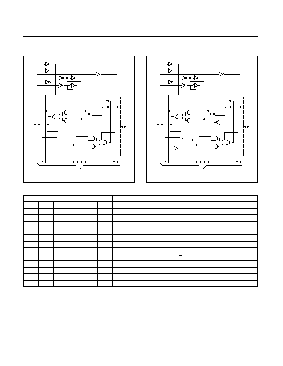
LOGIC DIAGRAM ≠ 74ALS651/651-1
VCC
=
Pin 24
GND = Pin 12
A0
OEBA
B0
1D
C1
1D
C1
1 OF 8 CHANNELS
TO 7 OTHER CHANNELS
21
4
20
3
23
22
1
2
OEAB
CPBA
SBA
SPAB
SAB
SC00134
LOGIC DIAGRAM ≠ 74ALS652/652-1
VCC
=
Pin 24
GND = Pin 12
A0
OEBA
B0
1D
C1
1D
C1
1 OF 8 CHANNELS
TO 7 OTHER CHANNELS
21
4
20
3
23
22
1
2
OEAB
CPBA
SBA
SPAB
SAB
SC00135
FUNCTION TABLE
INPUTS
DATA I/O
OPERATING MODE
OEAB
OEBA
CPAB
CPBA
SAB
SBA
An
Bn
74ALS651/74ALS651-1
74ALS652/74ALS652-1
L
H
H or L
H or L
X
X
Input
Input
Isolation
Isolation
L
H
X
X
Input
Input
Store A and B data
Store A and B data
X
H
H or L
X
X
Input
Unspecified*
Store A, hold B
Store A, hold B
H
H
L
X
Input
Output
Store A in both registers
Store A in both registers
L
X
H or L
X
S
Unspecified*
Input
Hold A, store B
Hold A, store B
L
L
X
L
Output
Input
Store B in both registers
Store B in both registers
L
L
X
X
X
L
Output
Input
Real time B data to A bus
Real time B data to A bus
L
L
X
H or L
X
H
Output
Input
Stored B data to A bus
Stored B data to A bus
H
H
X
X
L
X
Input
Output
Real time A data to B bus
Real time A data to B bus
H
H
H or L
X
H
X
Input
Output
Stored A data to B bus
Stored A data to B bus
H
L
H or L
H or L
H
H
Output
Output
Stored A data to B bus
Stored A data to B bus
H
L
H or L
H or L
H
H
Output
Output
Stored B data to A bus
Stored B data to A bus
NOTES:
H = High voltage level
L
= Low voltage level
X = Don't care
*
= The data output function may be enabled or disabled by various signals at the OE and DIR inputs. Data input functions are always
enabled, i.e., data at the bus pins will be stored on every Low-to-High transition of the clock.
= Low-to-High clock transition