2002 Feb 26
2
Philips Semiconductors
Product specification
Octal D-type flip-flop; positive edge-trigger;
3-state
74ALVC374
FEATURES
∑
Wide supply voltage range from 1.65 to 3.6 V
∑
Complies with JEDEC standard:
JESD8-7 (1.65 to 1.95 V)
JESD8-5 (2.3 to 2.7 V)
JESD8B/JESD36 (2.7 to 3.6 V).
∑
3.6 V tolerant inputs/outputs
∑
CMOS LOW power consumption
∑
Direct interface with TTL levels (2.7 to 3.6 V)
∑
Power-down mode
∑
Latch-up performance exceeds
250 mA
∑
ESD protection:
2000 V Human Body Model (JESD22-A 114-A)
200 V Machine Model (JESD22-A 115-A).
DESCRIPTION
The 74ALVC374 is a high-performance, low-power,
low-voltage, Si-gate CMOS device and superior to most
advanced CMOS compatible TTL families.
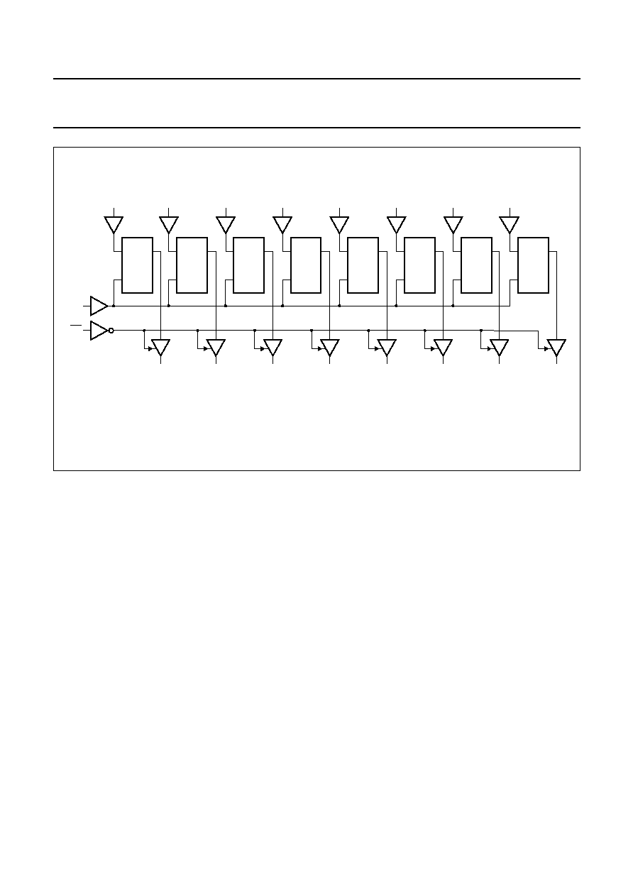
The 74ALVC374 is an octal D-type flip-flop featuring
separate D-type inputs for each flip-flop and 3-state
outputs for bus oriented applications. A clock (CP) input
and an output enable (OE) input are common to all
flip-flops.
The eight flip-flops will store the state of their individual
D-inputs that meet the set-up and hold times requirements
on the LOW-to-HIGH CP transition.
When OE is LOW, the contents of the eight flip-flops is
available at the outputs. When OE is HIGH, the outputs go
to the high-impedance OFF-state. Operation of the
OE input does not affect the state of the flip-flops.
The `374' is functionally identical to the `574', but the `574'
has a different pin arrangement.
QUICK REFERENCE DATA
GND = 0 V; T
amb
= 25
∞
C.
Notes
1. C
PD
is used to determine the dynamic power dissipation (P
D
in
µ
W).
P
D
= C
PD
◊
V
CC
2
◊
f
i
+ (C
L
◊
V
CC
2
◊
f
o
) where:
f
i
= input frequency in MHz;
f
o
= output frequency in MHz;
C
L
= output load capacitance in pF;
V
CC
= supply voltage in Volts.
2. The condition is V
I
= GND to V
CC
.
SYMBOL
PARAMETER
CONDITIONS
TYPICAL
UNIT
t
PHL
/t
PLH
propagation delay CP to Q
n
V
CC
= 1.8 V; C
L
= 30 pF; R
L
= 1 k
3.1
ns
V
CC
= 2.5 V; C
L
= 30 pF; R
L
= 500
2.3
ns
V
CC
= 2.7 V; C
L
= 50 pF; R
L
= 500
2.5
ns
V
CC
= 3.3 V; C
L
= 50 pF; R
L
= 500
2.5
ns
C
I
input capacitance
3.5
pF
C
PD
power dissipation capacitance per buffer
V
CC
= 3.3 V; notes 1 and 2
outputs enable
21
pF
outputs disabled
13
pF

2002 Feb 26
3
Philips Semiconductors
Product specification
Octal D-type flip-flop; positive edge-trigger;
3-state
74ALVC374
ORDERING INFORMATION
FUNCTION TABLE
See note 1.
Note
1. H = HIGH voltage level;
h = HIGH voltage level one set-up time prior to the HIGH-to-LOW CP transition;
L = LOW voltage level;
l = LOW voltage level one set-up time prior to the HIGH-to-LOW CP transition;
= LOW-to-HIGH clock transition;
Z = high-impedance OFF-state.
PINNING
TYPE NUMBER
PACKAGES
PINS
PACKAGE
MATERIAL
CODE
74ALVC374D
20
SO
plastic
SOT163-1
74ALVC374PW
20
TSSOP
plastic
SOT360-1
OPERATING MODES
INPUT
INTERNAL
FLIP-FLOPS
OUTPUTS
OE
CP
D
n
Q
0
to Q
7
Load and read register
L
l
L
L
L
h
H
H
Latch and read register
H
l
L
Z
H
h
H
Z
PIN
SYMBOL
DESCRIPTION
1
OE
output enable input (active LOW)
2, 5, 6, 9, 12, 15, 16, 19 Q
0
to Q
7
3-state flip-flop outputs
3, 4, 7, 8, 13, 14, 17, 18 D
0
to D
7
data inputs
10
GND
ground (0 V)
11
CP
clock input (LOW-to-HIGH, edge triggered)
20
V
CC
supply voltage