
2002 Feb 26
2
Philips Semiconductors
Product specification
Octal buffer/line driver; 3-state
74ALVC541
FEATURES
∑
Wide supply voltage range from 1.65 to 3.6 V
∑
Complies with JEDEC standard:
JESD8-7 (1.65 to 1.95 V)
JESD8-5 (2.3 to 2.7 V)
JESD8B/JESD36 (2.7 to 3.6 V).
∑
3.6 V tolerant inputs/outputs
∑
CMOS LOW power consumption
∑
Direct interface with TTL levels (2.7 to 3.6 V)
∑
Power-down mode
∑
Latch-up performance exceeds
250 mA
∑
ESD protection:
2000 V Human Body Model (JESD22-A114-A)
200 V Machine Model (JESD22-A115-A).
DESCRIPTION
The 74ALVC541 is a high-performance, low-power,
low-voltage, Si-gate CMOS device and superior to most
advanced CMOS compatible TTL families.
The 74ALVC541 is an octal non-inverting buffer/line driver
with 3-state bus compatible outputs. The 3-state outputs
are controlled by the output enable inputs OE
0
and OE
1
.
A HIGH on OE
n
causes the outputs to assume a
high-impedance OFF-state.
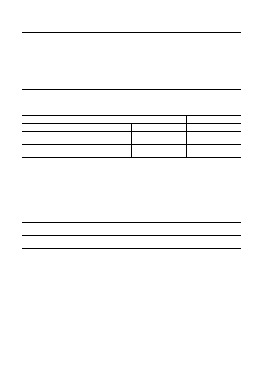
QUICK REFERENCE DATA
GND = 0 V; T
amb
= 25
∞
C.
Notes
1. C
PD
is used to determine the dynamic power dissipation (P
D
in
µ
W).
P
D
= C
PD
◊
V
CC
2
◊
f
i
+ (C
L
◊
V
CC
2
◊
f
o
) where:
f
i
= input frequency in MHz;
f
o
= output frequency in MHz;
C
L
= output load capacitance in pF;
V
CC
= supply voltage in Volts.
2. The condition is V
I
= GND to V
CC
.
SYMBOL
PARAMETER
CONDITIONS
TYPICAL
UNIT
t
PHL
/t
PLH
propagation delay inputs A
n
to Y
n
V
CC
= 1.8 V; C
L
= 30 pF; R
L
= 1 k
3.0
ns
V
CC
= 2.5 V; C
L
= 30 pF; R
L
= 500
2.2
ns
V
CC
= 2.7 V; C
L
= 50 pF; R
L
= 500
2.5
ns
V
CC
= 3.3 V; C
L
= 50 pF; R
L
= 500
2.3
ns
C
I
input capacitance
3.5
pF
C
I/O
input/output capacitance
3.5
pF
C
PD
power dissipation capacitance per buffer
V
CC
= 3.3 V; notes 1 and 2
outputs enable
25
pF
outputs disabled
0
pF
2002 Feb 26
3
Philips Semiconductors
Product specification
Octal buffer/line driver; 3-state
74ALVC541
ORDERING INFORMATION
FUNCTION TABLE
See note 1.
Note
1. H = HIGH voltage level;
L = LOW voltage level;
X = don't care;
Z = high-impedance OFF-state.
PINNING
TYPE NUMBER
PACKAGES
PINS
PACKAGE
MATERIAL
CODE
74ALVC541D
20
SO
plastic
SOT163-1
74ALVC541PW
20
TSSOP
plastic
SOT360-1
INPUT
OUTPUT
OE
0
OE
1
A
n
Y
n
L
L
L
L
L
L
H
H
X
H
X
Z
H
X
X
Z
PIN
SYMBOL
DESCRIPTION
1, 19
OE
0
, OE
1
output enable input (active LOW)
2, 3, 4, 5, 6, 7, 8, 9
A
0
to A
7
data input
10
GND
ground (0 V)
11, 12, 13, 14, 15, 16, 17, 18
Y
7
to Y
0
bus output
20
V
CC
supply voltage

2002 Feb 26
5
Philips Semiconductors
Product specification
Octal buffer/line driver; 3-state
74ALVC541
RECOMMENDED OPERATING CONDITIONS
LIMITING VALUES
In accordance with the Absolute Maximum Rating System (IEC 60134); voltages are referenced to GND (ground = 0 V).
Notes
1. The input and output voltage ratings may be exceeded if the input and output current ratings are observed.
2. When V
CC
= 0 V (Power-down mode), the output voltage can be 3.6 V in normal operation.
SYMBOL
PARAMETER
CONDITIONS
MIN.
MAX.
UNIT
V
CC
supply voltage
1.65
3.6
V
V
I
input voltage
0
3.6
V
V
O
output voltage
enable mode; V
CC
= 1.65 to 3.6 V 0
V
CC
V
disable mode; V
CC
= 1.65 to 3.6 V 0
3.6
V
Power-down mode; V
CC
= 0 V
0
3.6
V
T
amb
operating ambient temperature
-
40
+85
∞
C
t
r
, t
f
input rise and fall times
V
CC
= 1.65 to 2.7 V
0
20
ns/V
V
CC
= 2.7 to 3.6 V
0
10
ns/V
SYMBOL
PARAMETER
CONDITIONS
MIN.
MAX.
UNIT
V
CC
supply voltage
-
0.5
+4.6
V
I
IK
input diode current
V
I
< 0
-
-
50
mA
V
I
input voltage
-
0.5
+4.6
V
I
OK
output diode current
V
O
> V
CC
or V
O
< 0
-
±
50
mA
V
O
output voltage
enable mode; notes 1 and 2
-
0.5
V
CC
+ 0.5
V
disable mode
-
0.5
+4.6
V
Power-down mode; note 2
-
0.5
+4.6
V
I
O
output diode current
V
O
= 0 to V
CC
-
±
50
mA
I
GND
, I
CC
V
CC
or GND current
-
±
100
mA
T
stg
storage temperature
-
65
+150
∞
C
P
tot
power dissipation per package
SO package
above 70
∞
C derate linearly with
8 mW/K
-
500
mW
TSSOP package
above 60
∞
C derate linearly with
5.5 mW/K
-
500
mW

