2003 Jun 25
2
Philips Semiconductors
Product specification
Octal D-type transparent latch; 3-state
74ALVC573
FEATURES
∑
Wide supply voltage range from 1.65 to 3.6 V
∑
Complies with JEDEC standards:
JESD8-7 (1.65 to 1.95 V)
JESD8-5 (2.3 to 2.7 V)
JESD8B/JESD36 (2.7 to 3.6 V).
∑
3.6 V tolerant inputs and outputs
∑
CMOS low power consumption
∑
Direct interface with TTL levels (2.7 to 3.6 V)
∑
Power-down mode
∑
Latch-up performance exceeds 250 mA
∑
ESD protection:
HBM EIA/JESD22-A114-A exceeds 2000 V
MM EIA/JESD22-A115-A exceeds 200 V.
DESCRIPTION
The 74ALVC573 is a high-performance, low-power,
low-voltage, Si-gate CMOS device and superior to most
advanced CMOS compatible TTL families.
The 74ALVC573 is an octal D-type transparent latch
featuring separate D-type inputs for each latch and 3-state
outputs for bus oriented applications. A latch enable (LE)
input and an output enable (OE) input are common to all
internal latches.
The 74ALVC573 consists of eight D-type transparent
latches with 3-state true outputs. When LE is HIGH, data
at the Dn inputs enters the latches. In this condition the
latches are transparent, i.e. a latch output will change state
each time its corresponding D-input changes.
When LE is LOW the latches store the information that
was present at the D-inputs a set-up time preceding the
HIGH-to-LOW transition of LE. When OE is LOW, the
contents of the 8 latches are available at the outputs.
When OE is HIGH, the outputs go to the high-impedance
OFF-state. Operation of the OE input does not affect the
state of the latches.
The 74ALVC573 is functionally identical to the
74ALVC373, but the has a different pin arrangement.
QUICK REFERENCE DATA
GND = 0 V; T
amb
= 25
∞
C.
Notes
C
PD
is used to determine the dynamic power dissipation (P
D
in
µ
W).
P
D
= C
PD
◊
V
CC
2
◊
f
i
◊
N +
(C
L
◊
V
CC
2
◊
f
o
) where:
f
i
= input frequency in MHz;
f
o
= output frequency in MHz;
C
L
= output load capacitance in pF;
V
CC
= supply voltage in Volts;
N = total load switching outputs;
(C
L
◊
V
CC
2
◊
f
o
) = sum of the outputs.
1. The condition is V
I
= GND to V
CC
.
SYMBOL
PARAMETER
CONDITIONS
TYPICAL
UNIT
t
PHL
/t
PLH
propagation delay input Dn to output Qn
V
CC
= 1.8 V; C
L
= 30 pF; R
L
= 1 k
2.5
ns
V
CC
= 2.5 V; C
L
= 30 pF; R
L
= 500
2.0
ns
V
CC
= 2.7 V; C
L
= 50 pF; R
L
= 500
2.3
ns
V
CC
= 3.3 V; C
L
= 50 pF; R
L
= 500
2.2
ns
C
I
input capacitance
3.5
pF
C
PD
power dissipation capacitance per buffer
V
CC
= 3.3 V; notes and 1
outputs enabled
37
pF
outputs disabled
7
pF
2003 Jun 25
3
Philips Semiconductors
Product specification
Octal D-type transparent latch; 3-state
74ALVC573
FUNCTION TABLE
See note 1
Note
1. H = HIGH voltage level;
a) h = HIGH voltage level one set-up time prior to the HIGH-to-LOW LE transition;
b) L = LOW voltage level;
c) l = LOW voltage level one set-up time prior to the HIGH-to-LOW LE transition;
d) Z = high-impedance OFF-state.
ORDERING INFORMATION
OPERATING MODES
INPUT
INTERNAL
LATCH
OUTPUT
OE
LE
Dn
Qn
Enable and read register
(transparent mode)
L
H
L
L
L
L
H
H
H
H
Latch and read register
L
L
l
L
L
L
L
h
H
H
Latch register and disable
outputs
H
L
l
L
Z
H
L
h
H
Z
TYPE NUMBER
PACKAGE
TEMPERATURE
RANGE
PINS
PACKAGE
MATERIAL
CODE
74ALVC573D
-
40 to +85
∞
C
20
SO20
plastic
SOT163-1
74ALVC573PW
-
40 to +85
∞
C
20
TSSOP20
plastic
SOT360-1
74ALVC573BQ
-
40 to +85
∞
C
20
DHVQFN20
plastic
SOT764-1
PINNING
PIN
SYMBOL
DESCRIPTION
1
OE
output enable input (active
LOW)
2
D0
data input
3
D1
data input
4
D2
data input
5
D3
data input
6
D4
data input
7
D5
data input
8
D6
data input
9
D7
data input
10
GND
ground (0 V)
11
LE
latch enable input (active
HIGH)
12
Q7
3-state latch output
13
Q6
3-state latch output
14
Q5
3-state latch output
15
Q4
3-state latch output
16
Q3
3-state latch output
17
Q2
3-state latch output
18
Q1
3-state latch output
19
Q0
3-state latch output
20
V
CC
supply voltage
PIN
SYMBOL
DESCRIPTION
2003 Jun 25
4
Philips Semiconductors
Product specification
Octal D-type transparent latch; 3-state
74ALVC573
handbook, halfpage
OE
D0
D1
D2
D3
573
D4
D5
D6
D7
GND
VCC
Q0
Q1
Q2
Q4
Q5
Q3
Q6
Q7
LE
1
2
3
4
5
6
7
8
9
10
11
12
20
19
18
17
16
15
14
13
MNA806
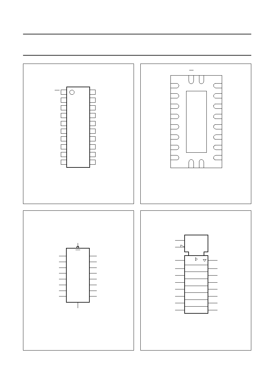
Fig.1 Pin configuration SO20 and TSSOP20.
handbook, halfpage
1
2
3
4
5
6
7
8
9
D0
D1
D2
D3
D4
D5
D6
D7
19
18
17
16
15
14
13
12
Q1
Q0
Q2
Q3
Q4
Q5
Q6
Q7
20
OE
VCC
10
11
GND
Top view
LE
GND
(1)
MNA979
Fig.2 Pin configuration DHVQFN20.
(1) The die substrate is attached to this pad using conductive die
attach material. It can not be used as a supply pin or input.
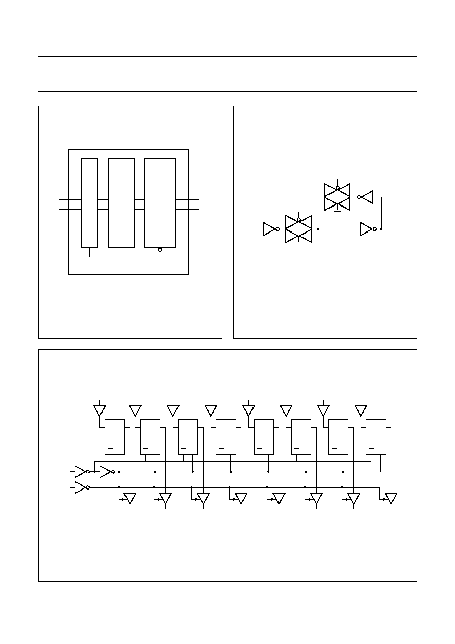
Fig.3 Logic symbol.
handbook, halfpage
MNA807
D0
D1
D2
D3
D4
D5
D6
D7
LE
OE
Q0
Q1
Q2
Q3
Q4
Q5
Q6
Q7
1
11
12
13
14
15
16
17
18
19
9
8
7
6
5
4
3
2
handbook, halfpage
MNA808
12
13
14
15
16
17
18
11
C1
1
EN1
1D
19
9
8
7
6
5
4
3
2
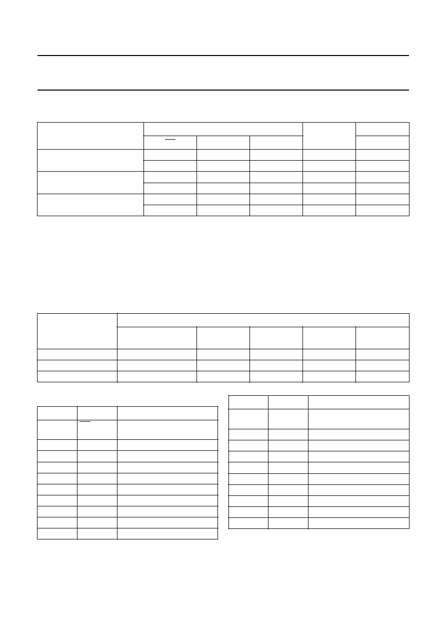
Fig.4 IEC logic symbol.