 | –≠–ª–µ–∫—Ç—Ä–æ–Ω–Ω—ã–π –∫–æ–º–ø–æ–Ω–µ–Ω—Ç: 74F175A | –°–∫–∞—á–∞—Ç—å:  PDF PDF  ZIP ZIP |
Philips
Semiconductors
74F175*, 74F175A
Quad D flip-flop
Product specification
IC15 Data Handbook
1996 Mar 12
INTEGRATED CIRCUITS
* Discontinued part. Please see the Discontinued Product List in Section 1, page 21.
Philips Semiconductors
Product specification
74F175A
Quad D flip-flop
2
1996 Mar 12
853≠0047 16555
FEATURES
∑
Four edge-triggered D-type flip-flops
∑
Buffered common clock
∑
Buffered asynchronous Master Reset
∑
True and complementary outputs
∑
Industrial temperature range available (≠40
∞
C to +85
∞
C)
∑
PNP light loading inputs
DESCRIPTION
The 74F175A is a quad, edge-triggered D-type flip-flop with
individual D inputs and both Q and Q outputs. The common buffered
Clock (CP) and Master Reset (MR) inputs load and reset (clear) all
flip-flops simultaneously.
The register is fully edge-triggered. The state of each D input, one
setup time before the Low-to-High clock transition is transferred to
the corresponding flip-flop's Q output.
All Q outputs will be forced Low independently of clock or data
inputs by a Low voltage level on the MR input. The device is useful
for applications where both true and complementary outputs are
required, and the CP and MR are common to all storage elements.
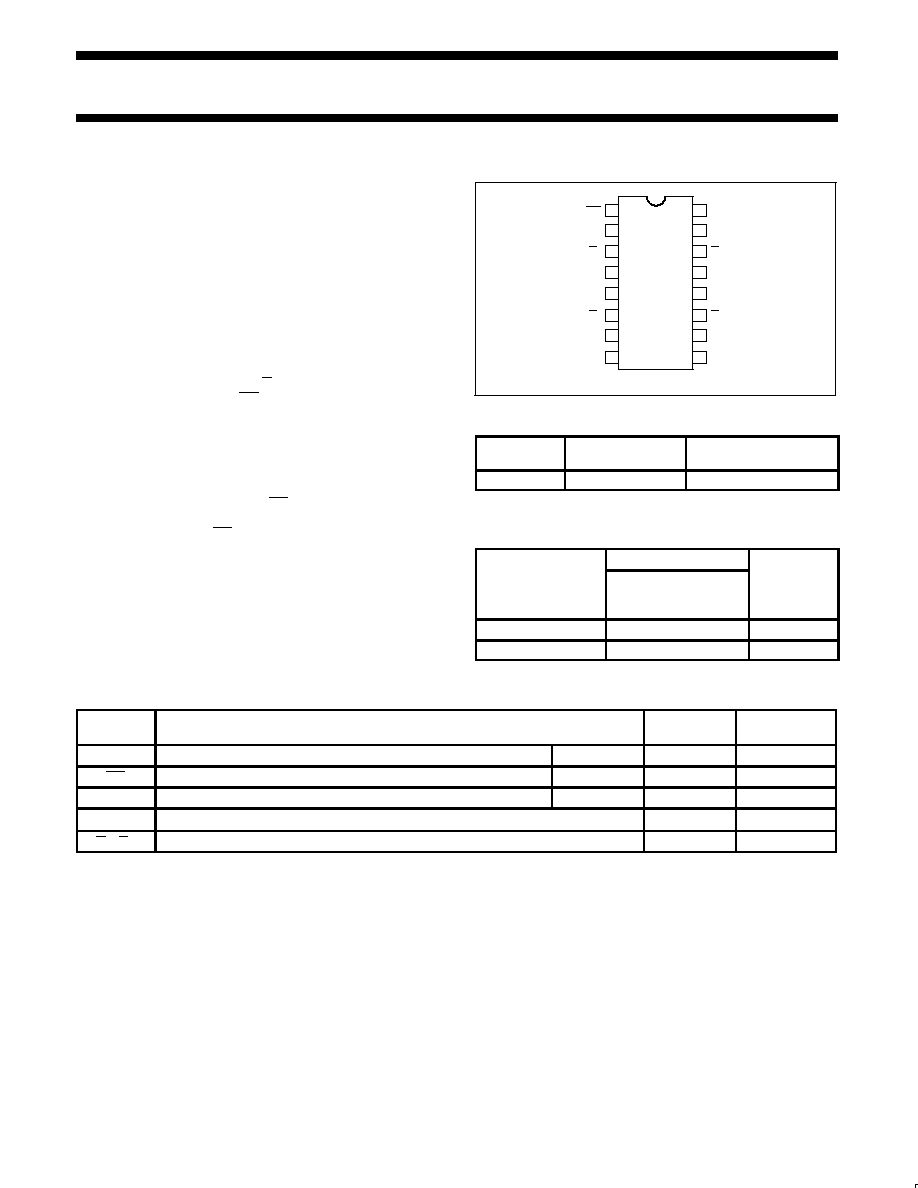
PIN CONFIGURATION
16
15
14
13
12
11
10
7
6
5
4
3
2
1
9
8
V
CC
SF00718
Q3
Q3
D3
D2
Q2
Q2
CP
MR
Q0
Q0
D0
D1
Q1
Q1
GND
TYPE
TYPICAL f
max
TYPICAL SUPPLY
CURRENT (TOTAL)
74F175A
160MHz
22mA
ORDERING INFORMATION
ORDER CODE
DESCRIPTION
COMMERCIAL RANGE
V
CC
= 5V
±
10%,
T
amb
= 0
∞
C to +70
∞
C
PKG. DWG. #
16-pin plastic DIP
74F175AN
SOT38-4
16-pin plastic SO
74F175AD
SOT109-1
INPUT AND OUTPUT LOADING AND FAN OUT TABLE
PINS
DESCRIPTION
74F (U.L.)
HIGH/LOW
LOAD VALUE
HIGH/LOW
D0 ≠ D3
Data inputs
74F175A
1.0/0.033
20
µ
A/20
µ
A
MR
Master reset input (active≠Low)
74F175A
1.0/0.033
20
µ
A/20
µ
A
CP
Clock input (active rising edge)
74F175A
1.0/0.033
20
µ
A/20
µ
A
Q0≠Q3
True outputs
50/33
1.0mA/20mA
Q0≠Q3
Complementary outputs
50/33
1.0mA/20mA
NOTE:
One (1.0) FAST unit load is defined as: 20
µ
A in the High state and 0.6mA in the Low state.

Philips Semiconductors
Product specification
74F175A
Quad D flip-flop
1996 Mar 12
3
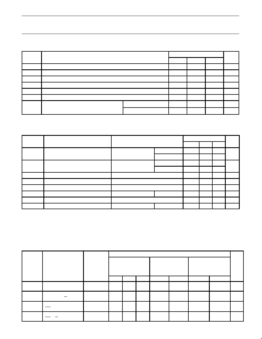
LOGIC SYMBOL
V
CC
= Pin 16
GND = Pin 8
SF00719
4
5
12 13
D0 D1 D2 D3
CP
MR
9
1
2
3
7
6
10
11 15
14
Q0 Q0 Q1 Q1 Q2 Q2 Q3 Q3
IEC/IEEE SYMBOL
R
C1
1D
SF00720
1
9
4
5
12
13
2
3
7
6
10
11
15
14
LOGIC DIAGRAM
D
Q
RD
V
CC
= Pin 16
GND = Pin 8
CP
D0
4
D
Q
RD
CP
D1
5
D
Q
RD
CP
D2
12
D
Q
RD
CP
D3
13
Q
SF00721
CP
MR
9
1
3
2
6
11
10
14
15
7
Q0
Q0
Q1
Q1
Q2
Q2
Q3
Q3
FUNCTION TABLE
INPUTS
OUTPUTS
OPERATING
MR
CP
Dn
Q
n
Q
n
MODE
L
X
X
L
H
Reset (clear)
H
h
H
L
Load "1"
H
I
L
H
Load "0"
H = High voltage level
h
= High state must be present one setup time before the
Low-to-High clock transition
L
= Low voltage level
l
= Low state must be present one setup time before the
Low-to-High clock transition
X = Don't care
= Low-to-High clock transition
ABSOLUTE MAXIMUM RATINGS
(Operation beyond the limit set forth in this table may impair the useful life of the device.
Unless otherwise noted these limits are over the operating free air temperature range.)
SYMBOL
PARAMETER
RATING
UNIT
V
CC
Supply voltage
≠0.5 to +7.0
V
V
IN
Input voltage
≠0.5 to +7.0
V
I
IN
Input current
≠30 to +5
mA
V
OUT
Voltage applied to output in High output state
≠0.5 to V
CC
V
I
OUT
Current applied to output in Low output state
40
mA
T
b
Operating free air temperature range
Commercial range
0 to +70
∞
C
T
amb
O erating free air tem erature range
Industrial range
≠40 to +85
∞
C
T
stg
Storage temperature range
≠65 to +150
∞
C
Philips Semiconductors
Product specification
74F175A
Quad D flip-flop
1996 Mar 12
4
RECOMMENDED OPERATING CONDITIONS
SYMBOL
PARAMETER
LIMITS
UNIT
MIN
NOM
MAX
V
CC
Supply voltage
4.5
5.0
5.5
V
V
IH
High-level input voltage
2.0
V
V
IL
Low-level input voltage
0.8
V
I
IK
Input clamp current
≠18
mA
I
OH
High-level output current
≠1
mA
I
OL
Low-level output current
20
mA
T
b
Operating free air temperature range
Commercial range
0
+70
∞
C
T
amb
Operating free air temperature range
Industrial range
≠40
+85
∞
C
DC ELECTRICAL CHARACTERISTICS
(Over recommended operating free-air temperature range unless otherwise noted.)
SYMBOL
PARAMETER
TEST
LIMITS
UNIT
CONDITIONS
1
MIN
TYP
2
MAX
V
OH
High-level output voltage
V
CC
= MIN, V
IL
= MAX,
"
10%V
CC
2.5
V
V
OH
High-level out ut voltage
CC
IL
V
IH
= MIN, I
OH
= MAX
"
5%V
CC
2.7
3.4
V
V
OL
Low-level output voltage
V
CC
= MIN, V
IL
= MAX,
"
10%V
CC
0.30
0.5
V
CC
IL
V
IH
= MIN, I
OL
= MAX
"
5%V
CC
0.30
0.5
V
V
IK
Input clamp voltage
V
CC
= MIN, I
I
= I
IK
≠0.73
≠1.2
V
I
I
Input current at maximum input voltage
V
CC
= 0.0V, V
I
= 7.0V
100
µ
A
I
IH
High-level input current
V
CC
= MAX, V
I
= 2.7V
20
µ
A
I
IL
Low-level input current
V
CC
= MAX, V
I
= 0.5V
74F175A
≠20
µ
A
I
OS
Short-circuit output current
3
V
CC
= MAX
≠60
≠150
mA
I
CC
Supply current (total)
V
CC
= MAX
74F175A
22
31
mA
Notes to DC electrical characteristics
1. For conditions shown as MIN or MAX, use the appropriate value specified under recommended operating conditions for the applicable type.
2. All typical values are at V
CC
= 5V, T
amb
= 25
∞
C.
3. Not more than one output should be shorted at a time. For testing I
OS
, the use of high-speed test apparatus and/or sample-and-hold
techniques are preferable in order to minimize internal heating and more accurately reflect operational values. Otherwise, prolonged shorting
of a high output may raise the chip temperature well above normal and thereby cause invalid readings in other parameter tests. In any
sequence of parameter tests, I
OS
tests should be performed last.
AC ELECTRICAL CHARACTERISTICS FOR 74F175A
LIMITS
T
amb
= 25
∞
C
T
amb
= 0
∞
C to +70
∞
C
T
amb
=
*
40
∞
C to +85
∞
C
SYMBOL
PARAMETER
TEST
V
CC
= +5V
V
CC
= +5.0V
±
10%
V
CC
= +5.0V
±
10%
UNIT
CONDITION
C
L
= 50pF,
R
L
= 500
C
L
= 50pF,
R
L
= 500
C
L
= 50pF,
R
L
= 500
MIN
TYP
MAX
MIN
MAX
MIN
MAX
f
max
Maximum clock
frequency
Waveform 1
140
160
125
110
MHz
t
PLH
t
PHL
Propagation delay
CP to Qn or Qn
Waveform 1
3.0
4.5
4.0
6.0
6.5
8.5
2.5
4.0
7.5
9.0
2.5
4.0
8.0
10.0
ns
t
PLH
t
PHL
Propagation delay
MR to Qn
Waveform 3
4.5
6.5
9.0
4.5
10.0
4.5
11.0
ns
t
PHL
t
PHL
Propagation delay
MR to Qn
Waveform 3
4.5
6.0
8.0
4.0
9.0
4.0
10.0
ns
Philips Semiconductors
Product specification
74F175A
Quad D flip-flop
1996 Mar 12
5
AC SETUP REQUIREMENTS FOR 74F175A
LIMITS
T
amb
= 25
∞
C
T
amb
= 0
∞
C to +70
∞
C
T
amb
=
*
40
∞
C to +85
∞
C
SYMBOL
PARAMETER
TEST
V
CC
= +5V
V
CC
= +5.0V
±
10%
V
CC
= +5.0V
±
10%
UNIT
CONDITION
C
L
= 50pF,
R
L
= 500
C
L
= 50pF,
R
L
= 500
C
L
= 50pF,
R
L
= 500
MIN
TYP
MAX
MIN
MAX
MIN
MAX
t
s
(H)
t
s
(L)
Setup time, High or Low
Dn to CP
Waveform 2
3.0
3.0
3.5
3.5
4.0
4.0
ns
t
h
(H)
t
h
(L)
Hold time, High or Low
Dn to CP
Waveform 2
0.0
0.0
0.0
0.0
0.0
0.0
ns
t
w
(H)
t
w
(L)
CP Pulse width
High or Low
Waveform 1
3.0
4.0
3.5
5.0
4.0
5.5
ns
t
w
(L)
MR Pulse width
Low
Waveform 3
3.5
3.5
4.0
ns
t
REC
Recovery time
MR to CP
Waveform 3
4.0
4.5
5.0
ns
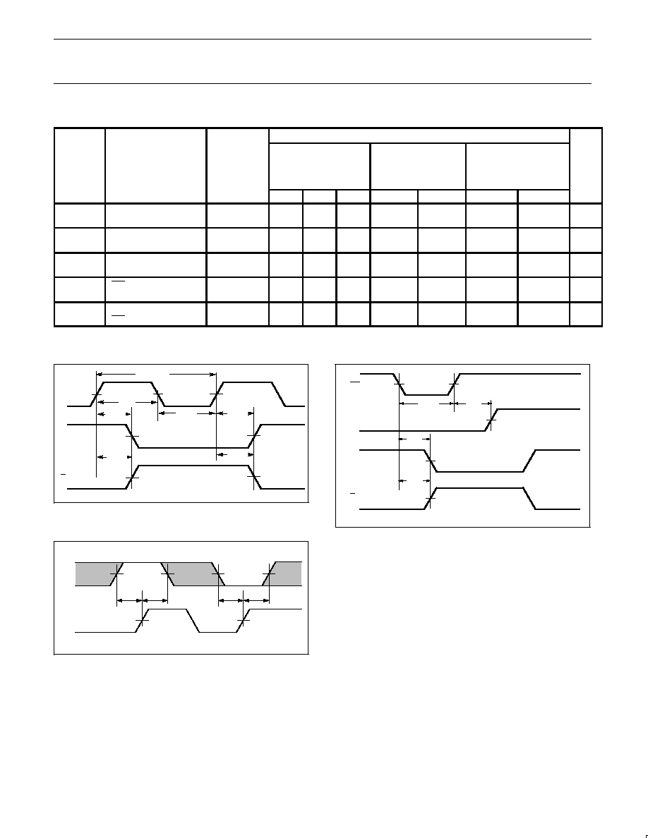
AC WAVEFORMS
For all waveforms, V
M
= 1.3V.
CP
V
M
V
M
V
M
t
w
(H)
1/f
max
V
M
V
M
t
PLH
t
w
(L)
t
PHL
Q
n
V
M
V
M
Q
n
t
PLH
t
PHL
SF00722
Waveform 1. Propagation delay for clock input to output, clock
pulse width, and maximum clock frequency
th(H)
ts(H)
CP
SF00191
VM
VM
VM
VM
VM
VM
th(L)
ts(L)
Dn
Waveform 2. Data setup time and hold times
CP
V
M
V
M
V
M
V
M
t
PHL
t
REC
MR
Q
n
t
w
(L)
V
M
Q
n
t
PLH
SF00723
Waveform 3. Master Reset pulse width, Master Reset to output
delay and Master Reset to Clock recovery time