 | –≠–ª–µ–∫—Ç—Ä–æ–Ω–Ω—ã–π –∫–æ–º–ø–æ–Ω–µ–Ω—Ç: 74HC164D | –°–∫–∞—á–∞—Ç—å:  PDF PDF  ZIP ZIP |

1.
General description
The 74HC164; 74HCT164 are high-speed Si-gate CMOS devices and are pin compatible
with Low power Schottky TTL (LSTTL). They are specified in compliance with JEDEC
standard no. 7A.
The 74HC164; 74HCT164 are 8-bit edge-triggered shift registers with serial data entry
and an output from each of the eight stages. Data is entered serially through one of two
inputs (DSA or DSB); either input can be used as an active HIGH enable for data entry
through the other input. Both inputs must be connected together or an unused input must
be tied HIGH.
Data shifts one place to the right on each LOW-to-HIGH transition of the clock (CP) input
and enters into Q0, which is the logical AND of the two data inputs (DSA and DSB) that
existed one set-up time prior to the rising clock edge.
A LOW level on the master reset (MR) input overrides all other inputs and clears the
register asynchronously, forcing all outputs LOW.
2.
Features
s
Gated serial data inputs
s
Asynchronous master reset
s
Complies with JEDEC standard no. 7A
s
ESD protection:
x
HBM EIA/JESD22-A114-B exceeds 2000 V
x
MM EIA/JESD22-A115-A exceeds 200 V.
s
Multiple package options
s
Specified from
-
40
∞
C to +85
∞
C and
-
40
∞
C to +125
∞
C.
3.
Quick reference data
74HC164; 74HCT164
8-bit serial-in, parallel-out shift register
Rev. 03 -- 4 April 2005
Product data sheet
Table 1:
Quick reference data
GND = 0 V; T
amb
= 25
∞
C; t
r
= t
f
= 6 ns.
Symbol
Parameter
Conditions
Min
Typ
Max
Unit
Type 74HC164
t
PHL
, t
PLH
propagation delay
CP to Qn
C
L
= 15 pF;
V
CC
= 5 V
-
12
-
ns
MR to Qn
C
L
= 15 pF;
V
CC
= 5 V
-
11
-
ns

9397 750 14693
© Koninklijke Philips Electronics N.V. 2005. All rights reserved.
Product data sheet
Rev. 03 -- 4 April 2005
2 of 24
Philips Semiconductors
74HC164; 74HCT164
8-bit serial-in, parallel-out shift register
[1]
C
PD
is used to determine the dynamic power dissipation (P
D
in
µ
W).
P
D
= C
PD
◊
V
CC
2
◊
f
i
◊
N +
(C
L
◊
V
CC
2
◊
f
o
) where:
f
i
= input frequency in MHz
f
o
= output frequency in MHz
N = number of inputs switching
(C
L
◊
V
CC
2
◊
f
o
) = sum of outputs
C
L
= output load capacitance in pF
V
CC
= supply voltage in Volts
[2]
For HC the condition is V
I
= GND to V
CC
.
[3]
For HCT the condition is V
I
= GND to V
CC
-
1.5 V.
4.
Ordering information
f
max
maximum clock frequency
C
L
= 15 pF;
V
CC
= 5 V
-
78
-
MHz
C
I
input capacitance
-
3.5
-
pF
C
PD
power dissipation
capacitance per package
[1]
[2]
-
40
-
pF
Type 74HCT164
t
PHL
, t
PLH
propagation delay
CP to Qn
C
L
= 15 pF;
V
CC
= 5 V
-
14
-
ns
MR to Qn
C
L
= 15 pF;
V
CC
= 5 V
-
16
-
ns
f
max
maximum clock frequency
C
L
= 15 pF;
V
CC
= 5 V
-
61
-
MHz
C
I
input capacitance
-
3.5
-
pF
C
PD
power dissipation
capacitance per package
[1]
[3]
-
40
-
pF
Table 1:
Quick reference data
...continued
GND = 0 V; T
amb
= 25
∞
C; t
r
= t
f
= 6 ns.
Symbol
Parameter
Conditions
Min
Typ
Max
Unit
Table 2:
Ordering information
Type number
Package
Temperature
range
Name
Description
Version
74HC164N
-
40
∞
C to +125
∞
C
DIP14
plastic dual in-line package; 14 leads (300 mil)
SOT27-1
74HC164D
-
40
∞
C to +125
∞
C
SO14
plastic small outline package; 14 leads; body width
3.9 mm; body thickness 1.47 mm
SOT108-2
74HC164DB
-
40
∞
C to +125
∞
C
SSOP14
plastic shrink small outline package; 14 leads; body
width 5.3 mm
SOT337-1
74HC164PW
-
40
∞
C to +125
∞
C
TSSOP14
plastic thin shrink small outline package; 14 leads; body
width 4.4 mm
SOT402-1
74HCT164N
-
40
∞
C to +125
∞
C
DIP14
plastic dual in-line package; 14 leads (300 mil)
SOT27-1
74HCT164D
-
40
∞
C to +125
∞
C
SO14
plastic small outline package; 14 leads; body width
3.9 mm; body thickness 1.47 mm
SOT108-2

9397 750 14693
© Koninklijke Philips Electronics N.V. 2005. All rights reserved.
Product data sheet
Rev. 03 -- 4 April 2005
3 of 24
Philips Semiconductors
74HC164; 74HCT164
8-bit serial-in, parallel-out shift register
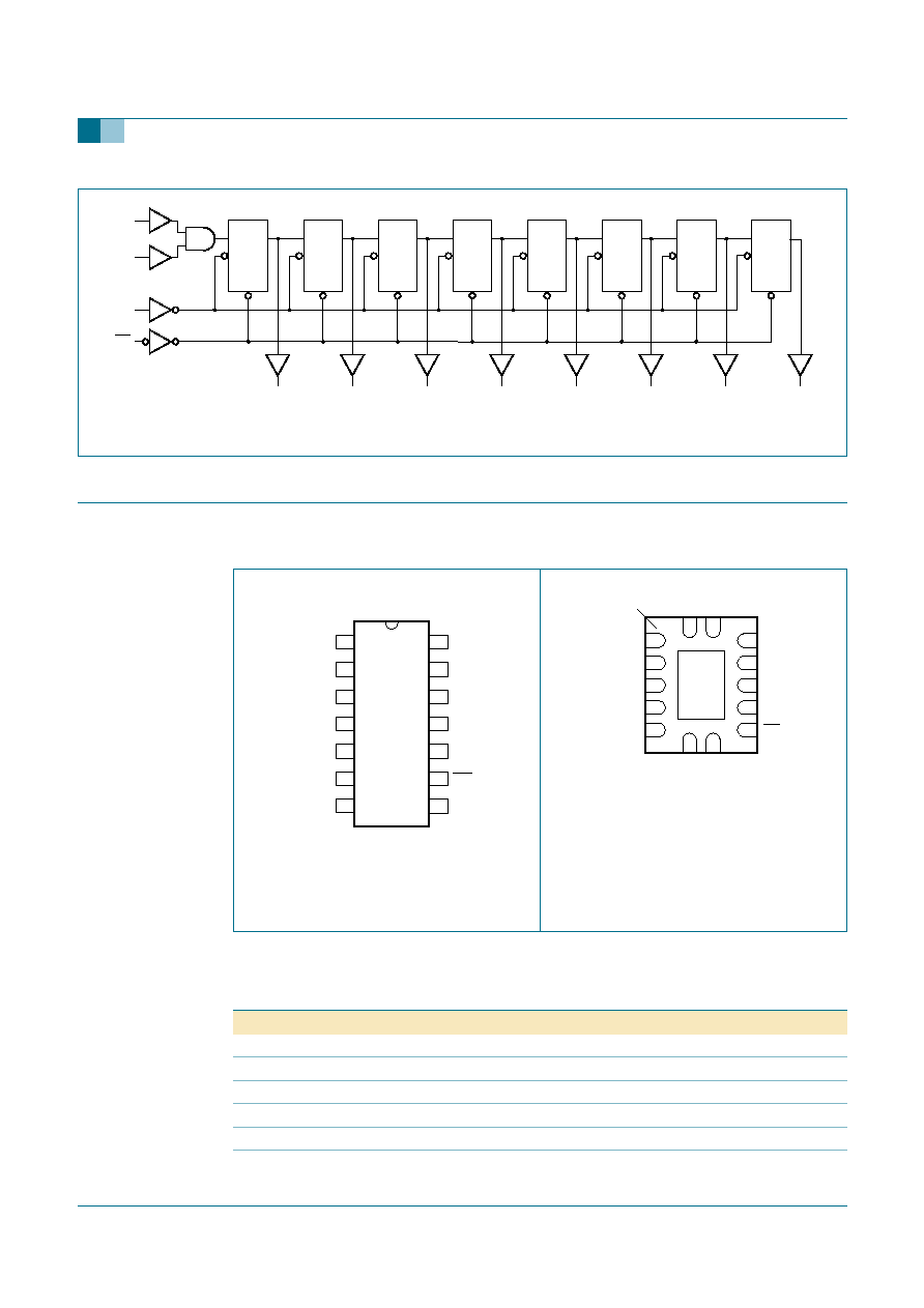
5.
Functional diagram
74HCT164DB
-
40
∞
C to +125
∞
C
SSOP14
plastic shrink small outline package; 14 leads; body
width 5.3 mm
SOT337-1
74HCT164PW
-
40
∞
C to +125
∞
C
TSSOP14
plastic thin shrink small outline package; 14 leads; body
width 4.4 mm
SOT402-1
74HCT164BQ
-
40
∞
C to +125
∞
C
DHVQFN14 plastic dual in-line compatible thermal enhanced very
thin quad flat package; no leads; 14 terminals; body
2.5
◊
3
◊
0.85 mm
SOT762-1
Table 2:
Ordering information
...continued
Type number
Package
Temperature
range
Name
Description
Version
Fig 1.
Logic symbol
Fig 2.
IEC logic symbol
Fig 3.
Logic diagram
001aac423
3
1
2
4
5
6
10
11
12
13
8
9
Q0
Q1
Q2
Q3
Q4
Q5
Q6
Q7
CP
DSB
DSA
MR
001aac424
9
8
&
3
1
2
4
5
6
10
11
13
12
R
C1/
1D
SRG8
001aac425
1
2
3
10
13
6
4
12
5
11
8
9
Q0 Q1 Q2
8-BIT SERIAL
-
IN/PARALLEL
-
OUT
SHIFT REGISTER
Q3 Q4 Q5 Q6 Q7
DSB
CP
MR
DSA
9397 750 14693
© Koninklijke Philips Electronics N.V. 2005. All rights reserved.
Product data sheet
Rev. 03 -- 4 April 2005
4 of 24
Philips Semiconductors
74HC164; 74HCT164
8-bit serial-in, parallel-out shift register
6.
Pinning information
6.1 Pinning
6.2 Pin description
Fig 4.
Functional diagram
001aac616
Q0
D
FF1
Q
CP
R
D
CP
DSB
DSA
MR
Q1
D
FF2
Q
CP
R
D
Q2
D
FF3
Q
CP
R
D
Q3
D
FF4
Q
CP
R
D
Q4
D
FF5
Q
CP
R
D
Q5
D
FF6
Q
CP
R
D
Q6
D
FF7
Q
CP
R
D
Q7
D
FF8
Q
CP
R
D
(1) The die substrate is attached to the
exposed die pad using conductive die
attach material. It can not be used as
a supply pin of input.
Fig 5.
Pin configuration DIP14, SO14,
SSOP14 and TSSOP14
Fig 6.
Pin configuration DHVQFN14
164
DSA
V
CC
DSB
Q7
Q0
Q6
Q1
Q5
Q2
Q4
Q3
MR
GND
CP
001aac422
1
2
3
4
5
6
7
8
10
9
12
11
14
13
001aac828
164
GND
(1)
Transparent top view
Q3
MR
Q2
Q4
Q1
Q5
Q0
Q6
DSB
Q7
GND
CP
DSA
V
CC
6
9
5
10
4
11
3
12
2
13
7
8
1
14
terminal 1
index area
Table 3:
Pin description
Symbol
Pin
Description
DSA
1
data input
DSB
2
data input
Q0
3
output
Q1
4
output
Q2
5
output
Q3
6
output

9397 750 14693
© Koninklijke Philips Electronics N.V. 2005. All rights reserved.
Product data sheet
Rev. 03 -- 4 April 2005
5 of 24
Philips Semiconductors
74HC164; 74HCT164
8-bit serial-in, parallel-out shift register
7.
Functional description
7.1 Function selection
[1]
H = HIGH voltage level
h = HIGH voltage level one set-up time prior to the LOW-to-HIGH clock transition
L = LOW voltage level
I = LOW voltage level one set-up time prior to the LOW-to-HIGH clock transition
q = lower case letters indicate the state of the referenced input one set-up time prior to the LOW-to-HIGH
clock transition
= LOW-to-HIGH clock transition
8.
Limiting values
GND
7
ground (0 V)
CP
8
clock input (LOW-to-HIGH, edge-triggered)
MR
9
master reset input (active LOW)
Q4
10
output
Q5
11
output
Q6
12
output
Q7
13
output
V
CC
14
positive supply voltage
Table 3:
Pin description
...continued
Symbol
Pin
Description
Table 4:
Function table
[1]
Operating
modes
Input
Output
MR
CP
DSA
DSB
Q0
Q1 to Q7
Reset (clear)
L
X
X
X
L
L to L
Shift
H
l
l
L
q0 to q6
H
l
h
L
q0 to q6
H
h
l
L
q0 to q6
H
h
h
H
q0 to q6
Table 5:
Limiting values
In accordance with the Absolute Maximum Rating System (IEC 60134). Voltages are referenced to
GND (ground = 0 V).
Symbol
Parameter
Conditions
Min
Max
Unit
V
CC
supply voltage
-
0.5
+7
V
I
IK
input diode current
V
I
<
-
0.5 V or
V
I
> V
CC
+ 0.5 V
-
±
20
mA
I
OK
output diode current
V
O
<
-
0.5 V or
V
O
> V
CC
+ 0.5 V
-
±
20
mA
I
O
output source or sink current
V
O
=
-
0.5 V to V
CC
+ 0.5 V
-
±
25
mA
I
CC
, I
GND
V
CC
or GND current
-
±
50
mA
T
stg
storage temperature
-
65
+150
∞
C