DATA SHEET
Product specification
File under Integrated Circuits, IC06
December 1990
INTEGRATED CIRCUITS
74HC/HCT182
Look-ahead carry generator
For a complete data sheet, please also download:
·
The IC06 74HC/HCT/HCU/HCMOS Logic Family Specifications
·
The IC06 74HC/HCT/HCU/HCMOS Logic Package Information
·
The IC06 74HC/HCT/HCU/HCMOS Logic Package Outlines
December 1990
2
Philips Semiconductors
Product specification
Look-ahead carry generator
74HC/HCT182
FEATURES
·
Provides carry look-ahead across a group of four ALU's
·
Multi-level look-ahead for high-speed arithmetic
operation over long word length
·
Output capability: standard
·
I
CC
category: MSI
GENERAL DESCRIPTION
The 74HC/HCT182 are high-speed Si-gate CMOS devices
and are pin compatible with low power Schottky TTL
(LSTTL). They are specified in compliance with JEDEC
standard no. 7A.
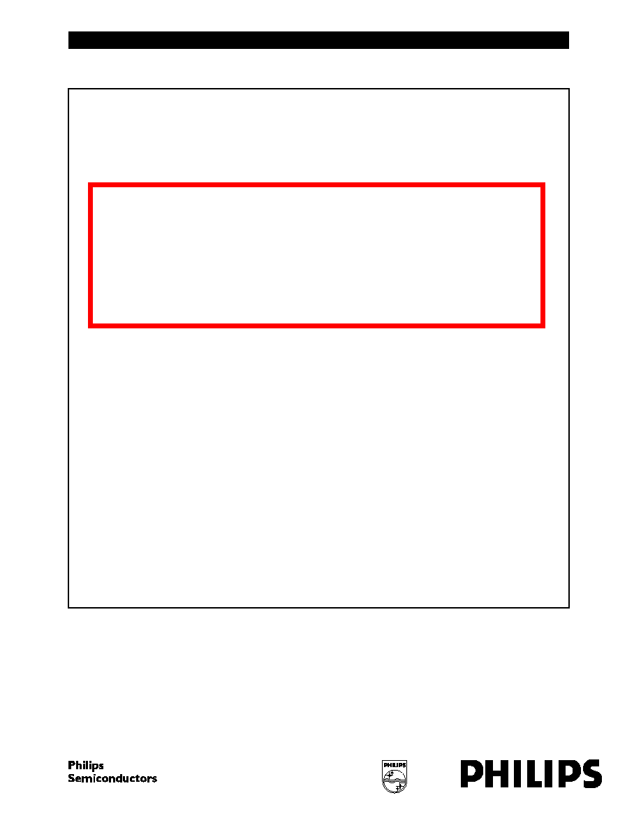
The 74HC/HCT182 carry look-ahead generators accept
up to four pairs of active LOW carry propagate (P
0
, P
1
, P
2
,
P
3
) and carry generate (G
0
, G
1
, G
2
, G
3
) signals and an
active HIGH carry input (C
n
). The devices provide
anticipated active HIGH carries (C
n
+
x
, C
n
+
y
, C
n
+
z
) across
four groups of binary adders.
The "182" also has active LOW carry propagate (P) and
carry generate (G) outputs which may be used for further
levels of look-ahead.
The logic equations provided at the outputs are:
C
n+x
= G
0
+ P
0
C
n
C
n+y
= G
1
+ P
1
G
0
+ P
1
P
0
C
n
C
n+z
= G
2
+ P
2
G
1
+ P
2
P
1
G
0
+ P
2
P
1
P
0
C
n
The "182" can also be used with binary ALU's in an active
LOW or active HIGH input operand mode. The
connections to and from the ALU to the carry look-ahead
generator are identical in both cases.
G
G
3
P
3
G
2
P
3
P
2
G
1
P
3
P
2
P
1
G
O
+
+
+
=
P
P
3
P
2
P
1
P
0
=
QUICK REFERENCE DATA
GND = 0 V; T
amb
= 25
°
C; t
r
= t
f
= 6 ns
Notes
1. C
PD
is used to determine the dynamic power dissipation (P
D
in
µ
W):
P
D
= C
PD
×
V
CC
2
×
f
i
+
(C
L
×
V
CC
2
×
f
o
) where:
f
i
= input frequency in MHz
f
o
= output frequency in MHz
(C
L
×
V
CC
2
×
f
o
) = sum of outputs
C
L
= output load capacitance in pF
V
CC
= supply voltage in V
2. For HC the condition is V
I
= GND to V
CC
For HCT the condition is V
I
= GND to V
CC
-
1.5 V
ORDERING INFORMATION
See
"74HC/HCT/HCU/HCMOS Logic Package Information"
.
SYMBOL
PARAMETER
CONDITIONS
TYPICAL
UNIT
HC
HCT
t
PHL
/ t
PLH
propagation delay
P
n
to P
C
n
to any output
P
n
or G
n
to any output
C
L
= 15 pF; V
CC
= 5 V
11
17
14
14
21
17
ns
ns
ns
C
I
input capacitance
3.5
3.5
pF
C
PD
power dissipation capacitance per
package
notes 1 and 2
50
50
pF
December 1990
3
Philips Semiconductors
Product specification
Look-ahead carry generator
74HC/HCT182
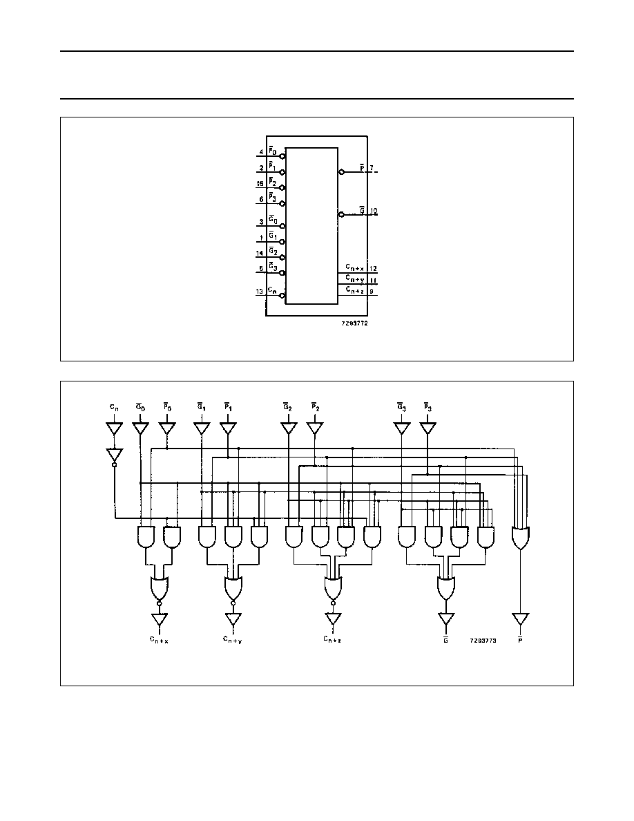
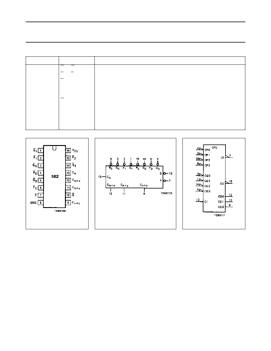
PIN DESCRIPTION
PIN NO.
SYMBOL
NAME AND FUNCTION
3, 1, 14, 5
G
0
to G
3
carry generate inputs (active LOW)
4, 2, 15, 6
P
0
to P
3
carry propagate inputs (active LOW)
7
P
carry propagate output (active LOW)
8
GND
ground (0 V)
9
C
n
+
z
function output
10
G
carry generate output (active LOW)
11
C
n
+
y
function output
12
C
n
+
x
function output
13
C
n
carry input (active HIGH)
16
V
CC
positive supply voltage
Fig.1 Pin configuration.
Fig.2 Logic symbol.
Fig.3 IEC logic symbol.
December 1990
5
Philips Semiconductors
Product specification
Look-ahead carry generator
74HC/HCT182
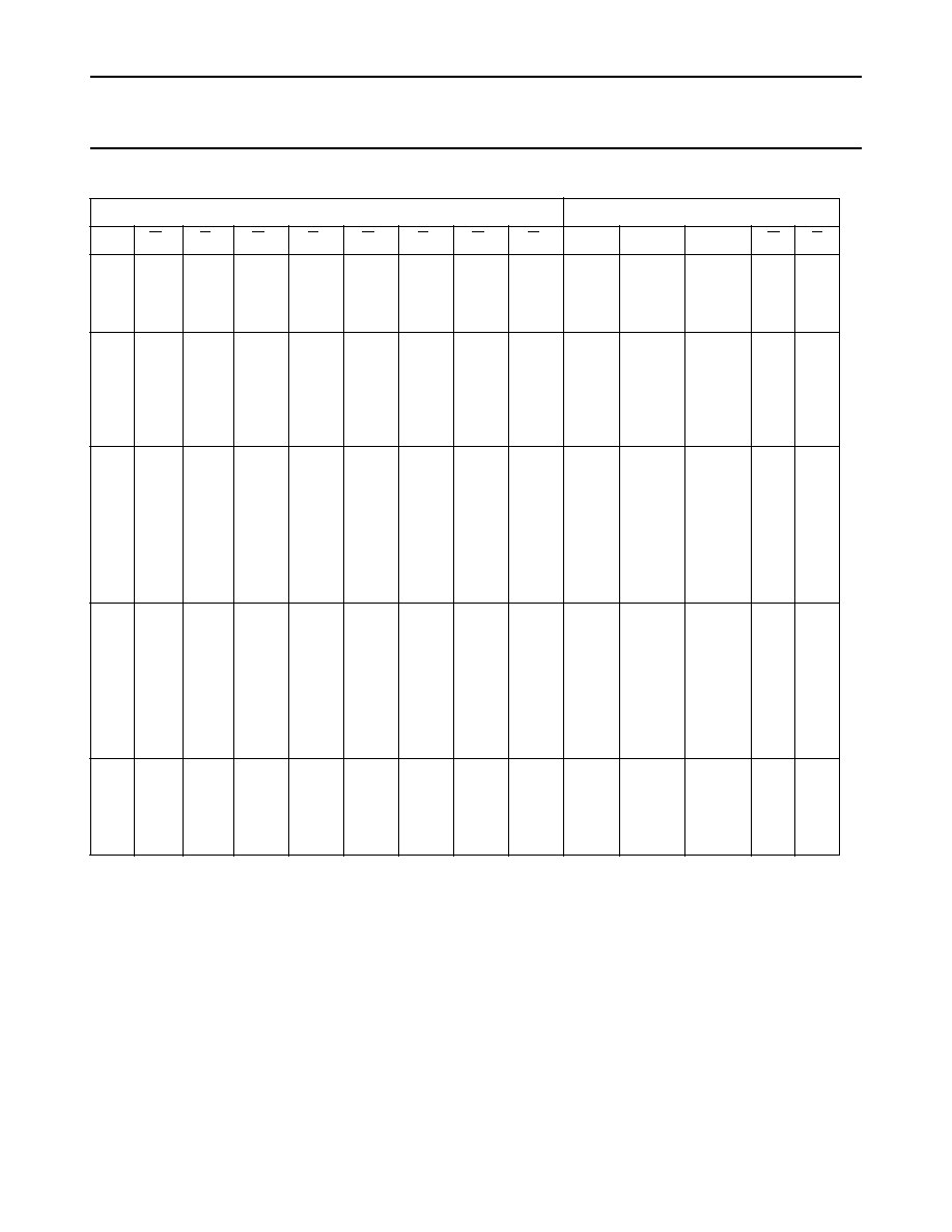
FUNCTION TABLE
Notes
1. H = HIGH voltage level
L = LOW voltage level
X = don't care
INPUTS
OUTPUTS
C
n
G
0
P
0
G
1
P
1
G
2
P
2
G
3
P
3
C
n
+
x
C
n
+
y
C
n
+
z
G
P
X
L
X
H
H
H
L
X
H
X
X
L
L
L
H
H
X
X
L
X
X
H
X
H
H
X
L
X
X
H
X
X
X
L
H
H
H
L
X
X
H
X
X
X
L
L
L
L
L
H
H
H
X
X
X
L
X
X
H
H
X
X
H
X
X
H
H
H
X
H
X
X
H
H
H
H
H
X
X
X
L
L
L
L
X
X
X
H
X
X
L
X
X
X
X
L
X
L
X
X
X
X
L
L
L
X
X
X
X
L
L
L
H
H
H
H
X
X
X
H
X
X
H
H
X
X
H
X
X
H
H
H
X
H
X
X
H
H
H
H
H
X
X
X
H
H
H
H
X
X
X
L
X
X
L
X
X
X
X
L
X
L
X
X
X
X
L
L
L
X
X
X
X
L
L
L
L
L
L
L
H
X
X
X
L
X
H
X
X
L
X
X
H
X
L
X
X
X
H
L
H
H
H
H
L