 | –≠–ª–µ–∫—Ç—Ä–æ–Ω–Ω—ã–π –∫–æ–º–ø–æ–Ω–µ–Ω—Ç: 74HC73DB | –°–∫–∞—á–∞—Ç—å:  PDF PDF  ZIP ZIP |

1.
General description
The 74HC73 is a high-speed Si-gate CMOS device and is pin compatible with low-power
Schottky TTL (LSTTL). The 74HC73 is specified in compliance with JEDEC
standard no. 7A.
The 74HC is a dual negative-edge triggered JK flip-flop featuring individual J, K, clock
(nCP) and reset (nR) inputs; also complementary nQ and nQ outputs.
The J and K inputs must be stable one set-up time prior to the HIGH-to-LOW clock
transition for predictable operation.
The reset (nR) is an asynchronous active LOW input. When LOW, it overrides the clock
and data inputs, forcing the nQ output LOW and the nQ output HIGH.
Schmitt-trigger action in the clock input makes the circuit highly tolerant to slower clock
rise and fall times.
2.
Features
s
Low-power dissipation
s
Complies with JEDEC standard no. 7A
s
ESD protection:
x
HBM EIA/JESD22-A114-B exceeds 2000 V
x
MM EIA/JESD22-A115-A exceeds 200 V.
s
Multiple package options
s
Specified from
-
40
∞
C to +80
∞
C and from
-
40
∞
C to +125
∞
C.
74HC73
Dual JK flip-flop with reset; negative-edge trigger
Rev. 03 -- 12 November 2004
Product data sheet

9397 750 13815
© Koninklijke Philips Electronics N.V. 2004. All rights reserved.
Product data sheet
Rev. 03 -- 12 November 2004
2 of 21
Philips Semiconductors
74HC73
Dual JK flip-flop with reset; negative-edge trigger
3.
Quick reference data
[1]
C
PD
is used to determine the dynamic power dissipation (P
D
in
µ
W).
P
D
= C
PD
◊
V
CC
2
◊
f
i
◊
N +
(C
L
◊
V
CC
2
◊
f
o
) where:
f
i
= input frequency in MHz;
f
o
= output frequency in MHz;
C
L
= output load capacitance in pF;
V
CC
= supply voltage in V;
N = number of inputs switching;
(C
L
◊
V
CC
2
◊
f
o
) = sum of outputs.
4.
Ordering information
Table 1:
Quick reference data
GND = 0 V; T
amb
= 25
∞
C; t
r
= t
f
= 6 ns.
Symbol
Parameter
Conditions
Min
Typ
Max
Unit
t
PHL
, t
PLH
propagation delay
C
L
= 15 pF; V
CC
= 5 V
-
-
nCP to nQ
-
16
-
ns
nCP to nQ
-
16
-
ns
nR to nQ, nQ
-
15
-
ns
f
max
maximum clock
frequency
C
L
= 15 pF; V
CC
= 5 V
-
77
-
MHz
C
I
input capacitance
-
3.5
-
pF
C
PD
power dissipation
capacitance per flip-flop
V
I
= GND to V
CC
[1]
-
30
-
pF
Table 2:
Ordering information
Type number
Package
Temperature range Name
Description
Version
74HC73N
-
40
∞
C to +125
∞
C
DIP14
plastic dual in-line package; 14 leads (300 mil)
SOT27-1
74HC73D
-
40
∞
C to +125
∞
C
SO14
plastic small outline package; 14 leads; body width 3.9 mm SOT108-1
74HC73DB
-
40
∞
C to +125
∞
C
SSOP14
plastic shrink small outline package; 14 leads; body width
5.3 mm
SOT337-1
74HC73PW
-
40
∞
C to +125
∞
C
TSSOP14 plastic thin shrink small outline package; 14 leads; body
width 4.4 mm
SOT402-1
9397 750 13815
© Koninklijke Philips Electronics N.V. 2004. All rights reserved.
Product data sheet
Rev. 03 -- 12 November 2004
3 of 21
Philips Semiconductors
74HC73
Dual JK flip-flop with reset; negative-edge trigger
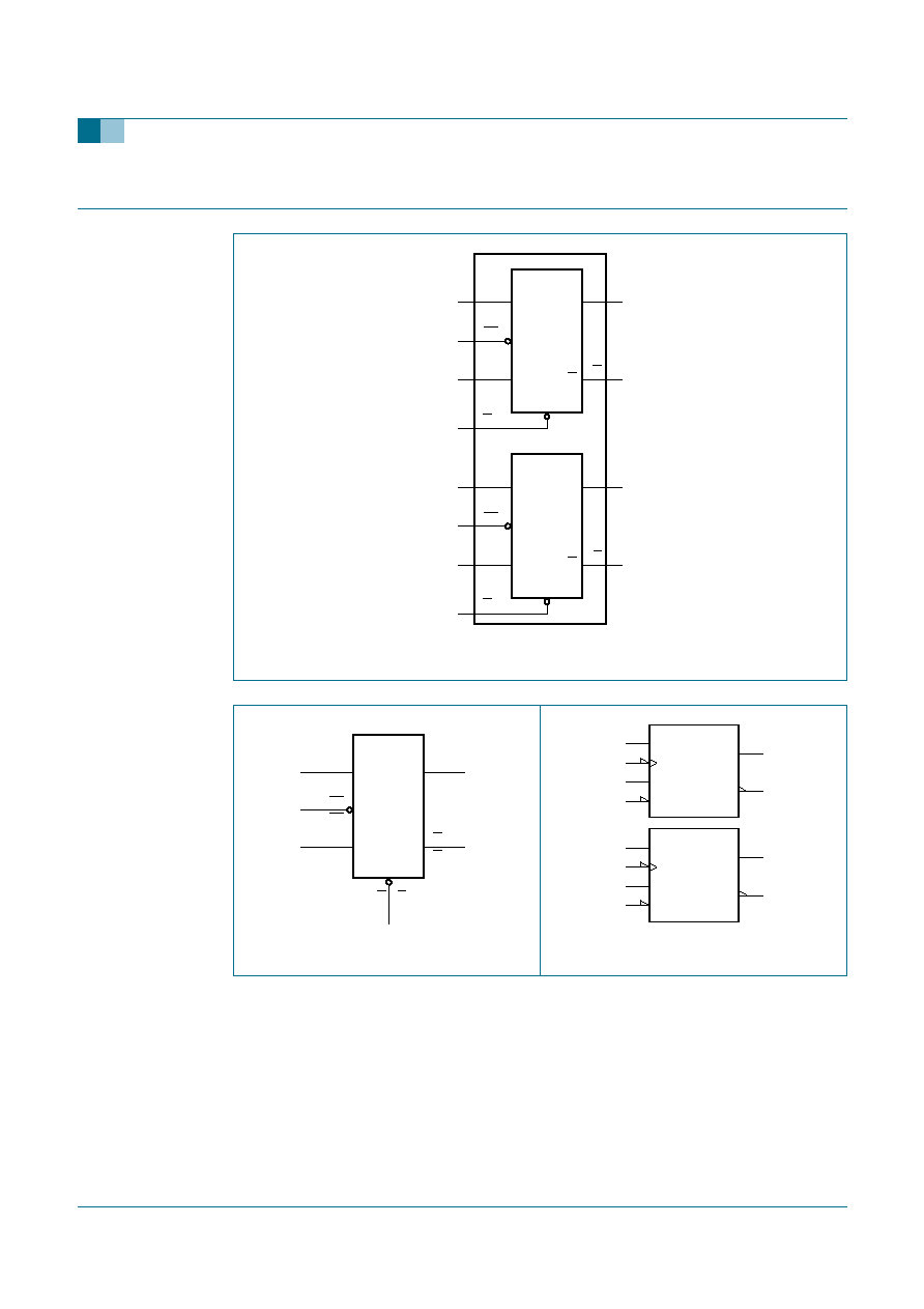
5.
Functional diagram
Fig 1.
Functional diagram
Fig 2.
Logic symbol
Fig 3.
IEC logic symbol
001aab981
Q
1Q 12
1J
14
Q
R
1Q 13
J
1CP
1
1K
3
1R
2
CP
FF1
K
Q
2Q 9
2J
7
Q
R
2Q 8
J
2CP
5
2K
10
2R
6
CP
FF2
K
001aab979
Q
1Q 12
2Q 9
1J
14
2J
7
Q
R
1Q 13
2Q 8
J
1CP
1
2CP
5
1K
3
2K
1R 2R
2 6
10
CP
FF
K
001aab980
13
12
1J
1K
3
R
2
1
4
C1
8
9
1J
1K
10
R
6
5
7
C1
9397 750 13815
© Koninklijke Philips Electronics N.V. 2004. All rights reserved.
Product data sheet
Rev. 03 -- 12 November 2004
4 of 21
Philips Semiconductors
74HC73
Dual JK flip-flop with reset; negative-edge trigger
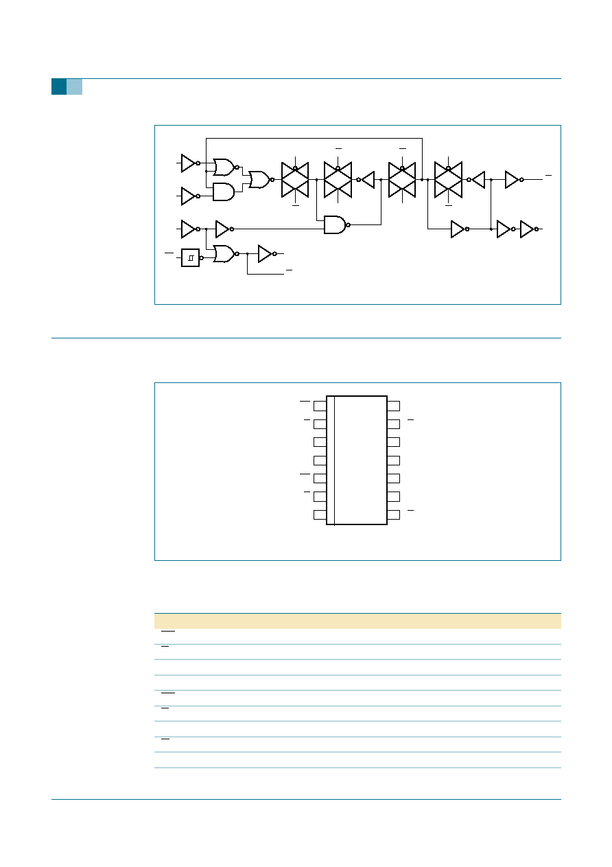
6.
Pinning information
6.1 Pinning
6.2 Pin description
Fig 4.
Logic diagram (one flip-flop)
001aab982
C
C
K
J
R
CP
C
C
C
C
C
C
C
C
Q
Q
Fig 5.
Pin configuration
73
1CP
1J
1R
1Q
1K
1Q
V
CC
GND
2CP
2K
2R
2Q
2J
2Q
001aab978
1
2
3
4
5
6
7
8
10
9
12
11
14
13
Table 3:
Pin description
Symbol
Pin
Description
1CP
1
clock input for flip-flop 1 (HIGH-to-LOW, edge-triggered)
1R
2
asynchronous reset input for flip-flop 1 (active LOW)
1K
3
synchronous K input for flip-flop 1
V
CC
4
positive supply voltage
2CP
5
clock input for flip-flop 2 (HIGH-to-LOW, edge-triggered)
2R
6
asynchronous reset input for flip-flop 2 (active LOW)
2J
7
synchronous J input for flip-flop 2
2Q
8
complement flip-flop 2 output
2Q
9
true flip-flop 2 output
2K
10
synchronous K input for flip-flop 2

9397 750 13815
© Koninklijke Philips Electronics N.V. 2004. All rights reserved.
Product data sheet
Rev. 03 -- 12 November 2004
5 of 21
Philips Semiconductors
74HC73
Dual JK flip-flop with reset; negative-edge trigger
7.
Functional description
7.1 Function table
[1]
H = HIGH voltage level;
h = HIGH voltage level one set-up time prior to the HIGH-to-LOW CP transition;
L = LOW voltage level;
I = LOW voltage level one set-up time prior to the HIGH-to-LOW CP transition;
q = state of referenced output one set-up time prior to the HIGH-to-LOW CP transition;
X = don't care;
= HIGH-to-LOW CP transition.
8.
Limiting values
[1]
Above 70
∞
C: P
tot
derates linearly with 12 mW/K.
[2]
Above 70
∞
C: P
tot
derates linearly with 8 mW/K.
GND
11
ground (0 V)
1Q
12
true flip-flop 1 output
1Q
13
complement flip-flop 1 output
1J
14
synchronous J input for flip-flop 1
Table 3:
Pin description
...continued
Symbol
Pin
Description
Table 4:
Function table
[1]
Input
Output
Operating mode
nR
nCP
nJ
nK
nQ
nQ
L
X
X
X
L
H
asynchronous reset
H
h
h
q
q
toggle
l
h
L
H
load 0 (reset)
h
l
H
L
load 1 (set)
l
l
q
q
hold (no change)
Table 5:
Limiting values
In accordance with the Absolute Maximum Rating System (IEC 60134). Voltages are referenced to
GND (ground = 0 V).
Symbol
Parameter
Conditions
Min
Max
Unit
V
CC
supply voltage
-
0.5
+7
V
I
IK
input diode current
V
I
<
-
0.5 V or V
I
> V
CC
+ 0.5 V
-
±
20
mA
I
OK
output diode current
V
O
<
-
0.5 V or V
O
> V
CC
+ 0.5 V
-
±
20
mA
I
O
output source or sink
current
V
O
=
-
0.5 V to V
CC
+ 0.5 V
-
±
25
mA
I
CC
, I
GND
V
CC
or GND current
-
±
50
mA
T
stg
storage temperature
-
65
+150
∞
C
P
tot
power dissipation
DIP14 package
[1]
-
750
mW
SO14, SSOP14 and
TSSOP14 packages
[2]
-
500
mW