
DATA SHEET
Product specification
File under Integrated Circuits, IC06
September 1993
INTEGRATED CIRCUITS
74HC/HCT139
Dual 2-to-4 line
decoder/demultiplexer
For a complete data sheet, please also download:
∑
The IC06 74HC/HCT/HCU/HCMOS Logic Family Specifications
∑
The IC06 74HC/HCT/HCU/HCMOS Logic Package Information
∑
The IC06 74HC/HCT/HCU/HCMOS Logic Package Outlines

September 1993
2
Philips Semiconductors
Product specification
Dual 2-to-4 line decoder/demultiplexer
74HC/HCT139
FEATURES
∑
Demultiplexing capability
∑
Two independent 2-to-4 decoders
∑
Multifunction capability
∑
Active LOW mutually exclusive outputs
∑
Output capability: standard
∑
I
CC
category: MSI
GENERAL DESCRIPTION
The 74HC/HCT139 are high-speed Si-gate CMOS devices
and are pin compatible with low power Schottky TTL
(LSTTL). It is specified in compliance with JEDEC
standard no. 7A.
The 74HC/HCT139 are high-speed, dual 2-to-4 line
decoder/multiplexers. This device has two independent
decoders, each accepting two binary weighted inputs
(nA
0
and nA
1
) and providing four mutually exclusive active
LOW outputs (nY
0
to nY3). Each decoder has an active
LOW enable input (nE).
When nE is HIGH, every output is forced HIGH. The
enable can be used as the data input for a 1-to-4
demultiplexer application.
The "139" is identical to the HEF4556 of the HE4000B
family.
QUICK REFERENCE DATA
GND = 0 V; T
amb
= 25
∞
C; t
r
= t
f
= 6 ns
Notes
1. C
PD
is used to determine the dynamic power dissipation (P
D
in
µ
W):
P
D
= C
PD
◊
V
CC
2
◊
f
i
+
(C
L
◊
V
CC
2
◊
f
o
) where:
f
i
= input frequency in MHz
f
o
= output frequency in MHz
(C
L
◊
V
CC
2
◊
f
o
) = sum of outputs
C
L
= output load capacitance in pF
V
CC
= supply voltage in V
2. For HC the condition is V
I
= GND to V
CC
For HCT the condition is V
I
= GND to V
CC
-
1.5 V
APPLICATIONS
∑
Memory decoding or data-routing
∑
Code conversion
ORDERING INFORMATION
See
"74HC/HCT/HCU/HCMOS Logic Package Information"
.
SYMBOL
PARAMETER
CONDITIONS
TYPICAL
UNIT
HC
HCT
t
PHL
/ t
PLH
propagation delay
C
L
= 15 pF; V
CC
= 5 V
nA
n
to nY
n
11
13
ns
nE
3
to nY
n
10
13
ns
C
I
input capacitance
3.5
3.5
pF
C
PD
power dissipation capacitance per multiplexer
notes 1 and 2
42
44
pF
September 1993
4
Philips Semiconductors
Product specification
Dual 2-to-4 line decoder/demultiplexer
74HC/HCT139
FUNCTION TABLE
Notes
1. H = HIGH voltage level
L = LOW voltage level
X = don't care
INPUTS
OUTPUTS
nE
nA
0
nA
1
nY
0
nY
1
nY
2
nY
3
H
X
X
H
H
H
H
L
L
L
L
L
H
L
H
L
L
H
H
L
H
H
H
H
L
H
H
H
H
L
H
H
H
H
L
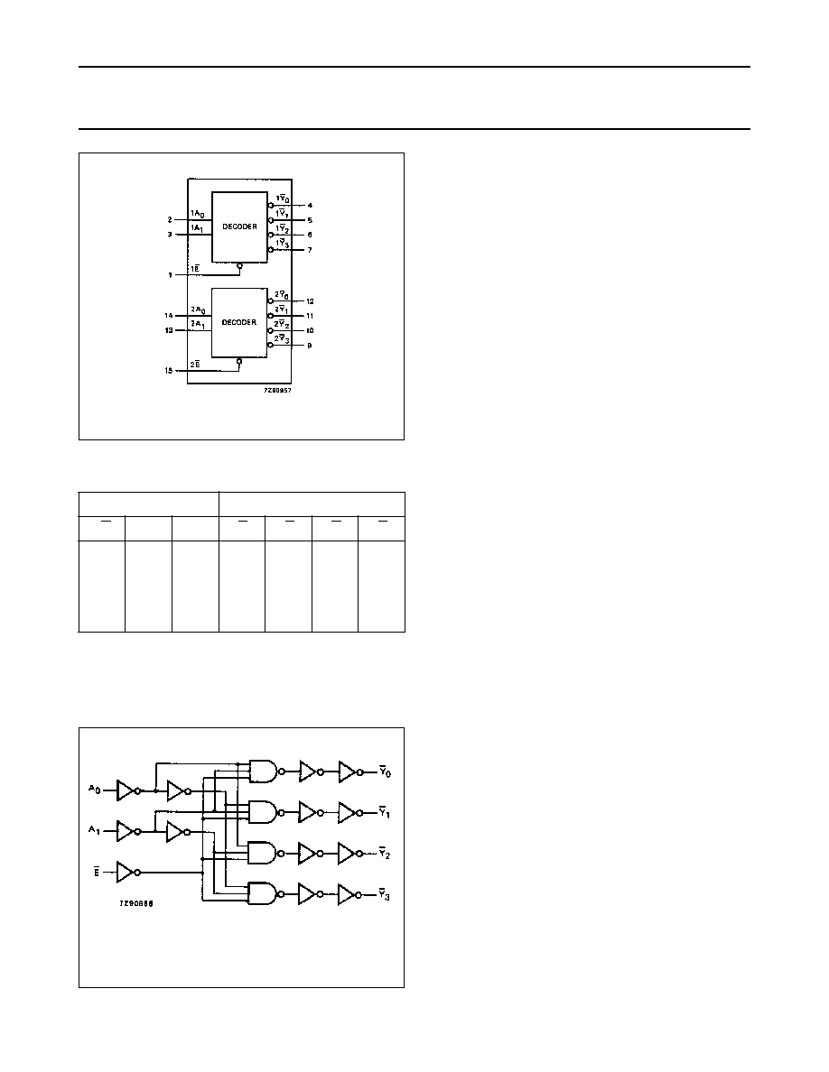
Fig.4 Functional diagram.
Fig.5 Logic diagram (one decoder/demultiplexer).

September 1993
5
Philips Semiconductors
Product specification
Dual 2-to-4 line decoder/demultiplexer
74HC/HCT139
DC CHARACTERISTICS FOR 74HC
For the DC characteristics see
"74HC/HCT/HCU/HCMOS Logic Family Specifications"
.
Output capability: standard
I
CC
category: MSI
AC CHARACTERISTICS FOR 74HC
GND = 0 V; t
r
= t
f
= 6 ns; C
L
= 50 pF
SYMBOL
PARAMETER
T
amb
(
∞
C)
UNIT
TEST CONDITIONS
74HC
V
CC
(V)
WAVEFORMS
+
25
-
40 to
+
85
-
40 to
+
125
min.
typ.
max.
min.
max.
min.
max.
t
PHL
/ t
PLH
propagation delay
nA
n
to Y
n
39
14
11
145
29
25
180
36
31
220
44
38
ns
2.0
4.5
6.0
Fig.6
t
PHL
/ t
PLH
propagation delay
nE to nY
n
33
12
10
135
27
23
170
34
29
205
41
35
ns
2.0
4.5
6.0
Fig.7
t
THL
/ t
TLH
output transition
time
19
7
6
75
15
13
95
19
16
110
22
19
ns
2.0
4.5
6.0
Figs 6 and 7
