2002 May 15
2
Philips Semiconductors
Product specification
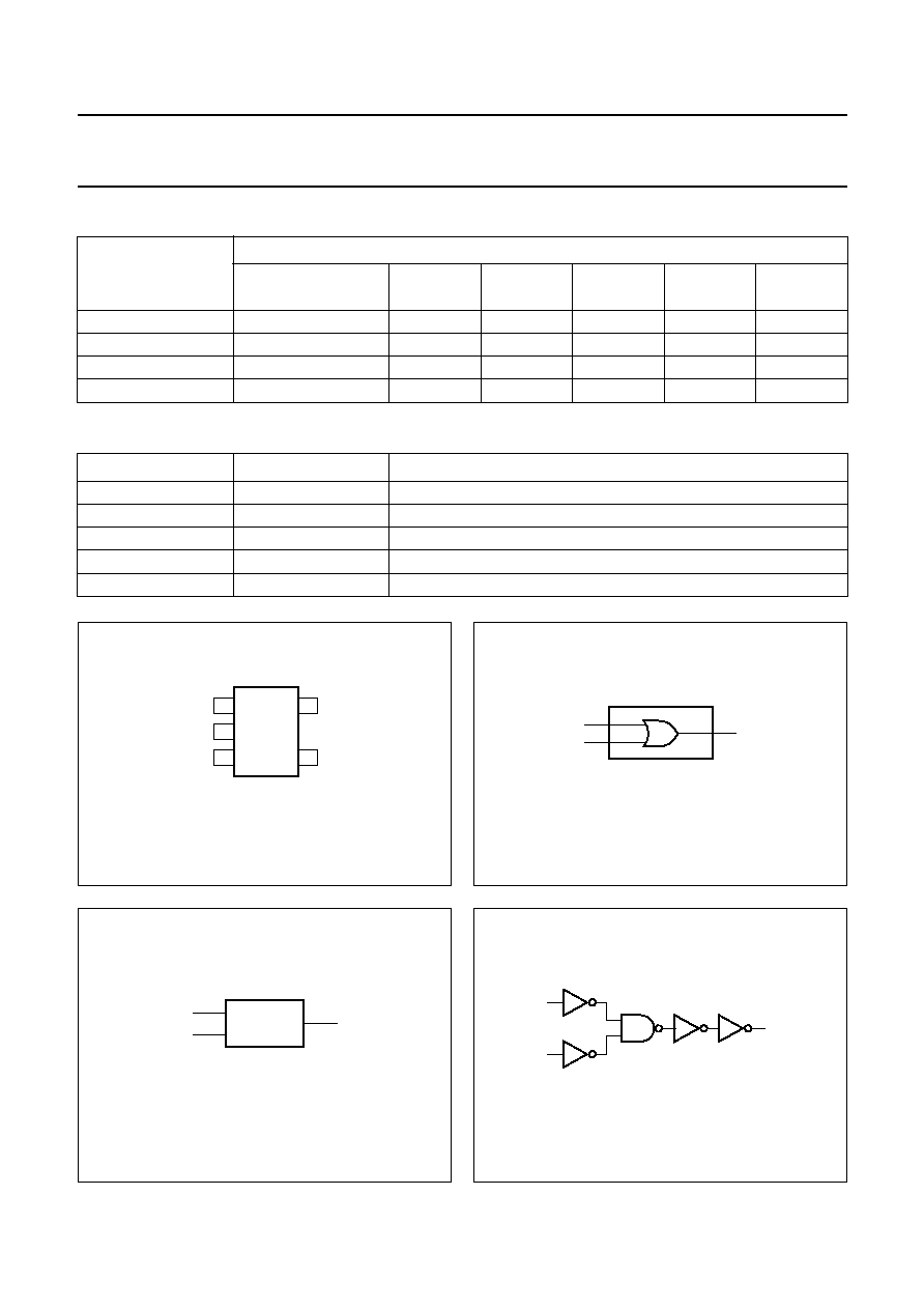
2-input OR gate
74HC1G32; 74HCT1G32
FEATURES
·
Wide operating voltage from 2.0 to 6.0 V
·
Symmetrical output impedance
·
High noise immunity
·
Low power dissipation
·
Balanced propagation delays
·
Very small 5 pins package
·
Output capability: standard.
DESCRIPTION
The 74HC1G/HCT1G32 is a highspeed Si-gate CMOS
device.
The 74HC1G/HCT1G32 provides the 2-input OR function.
The standard output currents are
1
/
2
compared to the
74HC/HCT32.
QUICK REFERENCE DATA
GND = 0 V; T
amb
= 25
°
C; t
r
= t
f
6.0 ns.
Notes
1. C
PD
is used to determine the dynamic power dissipation (P
D
in
µ
W).
P
D
= C
PD
×
V
CC
2
×
f
i
+ (C
L
×
V
CC
2
×
f
o
) where:
f
i
= input frequency in MHz;
f
o
= output frequency in MHz;
C
L
= output load capacitance in pF;
V
CC
= supply voltage in Volts.
2. For HC1G the conditions is V
I
= GND to V
CC
.
For HCT1G the conditions is V
I
= GND to V
CC
-
1.5 V.
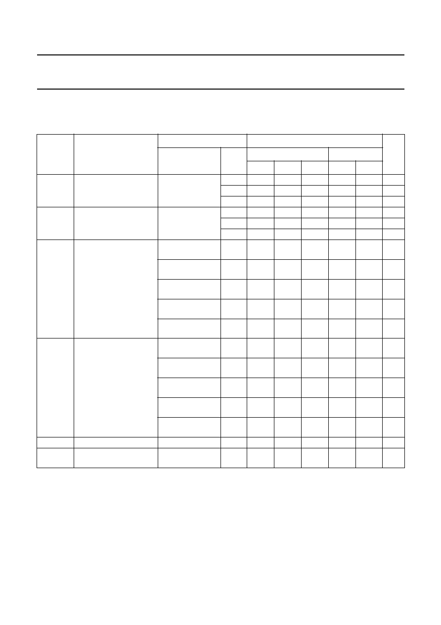
FUNCTION TABLE
See note 1.
Note
1. H = HIGH voltage level;
L = LOW voltage level.
SYMBOL
PARAMETER
CONDITIONS
TYPICAL
UNIT
HC1G
HCT1G
t
PHL
/t
PLH
propagation delay A and B to Y
C
L
= 15 pF; V
CC
= 5 V
8
10
ns
C
I
input capacitance
1.5
1.5
pF
C
PD
power dissipation capacitance
notes 1 and 2
19
20
pF
INPUTS
OUTPUT
A
B
Y
L
L
L
L
H
H
H
L
H
H
H
H
2002 May 15
4
Philips Semiconductors
Product specification
2-input OR gate
74HC1G32; 74HCT1G32
RECOMMENDED OPERATING CONDITIONS
LIMITING VALUES
In accordance with the Absolute Maximum Rating System (IEC 60134); voltages are referenced to GND (ground = 0 V);
notes 1 and 2.
Notes
1. Stresses beyond those listed may cause permanent damage to the device. These are stress rating only and
functional operation of the device at these or any other conditions beyond those under `recommended operating
conditions' is not implied. Exposure to absolute maximum rated conditions for extended periods may affect device
reliability.
2. The input and output voltage ratings may be exceeded if the input and output current ratings are observed.
3. Above 55
°
C the value of P
D
derates linearly with 2.5 mW/K.
SYMBOL
PARAMETER
CONDITIONS
74HC1G
74HCT1G
UNIT
MIN.
TYP.
MAX.
MIN.
TYP.
MAX.
V
CC
supply voltage
2.0
5.0
6.0
4.5
5.0
5.5
V
V
I
input voltage
0
-
V
CC
0
-
V
CC
V
V
O
output voltage
0
-
V
CC
0
-
V
CC
V
T
amb
operating ambient
temperature
see DC and AC
characteristics per
device
-
40
+25
+125
-
40
+25
+125
°
C
t
r
, t
f
input rise and fall
times
V
CC
= 2.0 V
-
-
1000
-
-
-
ns
V
CC
= 4.5 V
-
-
500
-
-
500
ns
V
CC
= 6.0 V
-
-
400
-
-
-
ns
SYMBOL
PARAMETER
CONDITIONS
MIN.
MAX.
UNIT
V
CC
supply voltage
-
0.5
+7.0
V
I
IK
input diode current
V
I
<
-
0.5 V or V
I
> V
CC
+ 0.5 V
-
±
20
mA
I
OK
output diode current
V
O
<
-
0.5 V or V
O
> V
CC
+ 0.5 V
-
±
20
mA
I
O
output source or sink current
-
0.5 V < V
O
< V
CC
+ 0.5 V
-
±
12.5
mA
I
CC
V
CC
or GND current
-
±
25
mA
T
stg
storage temperature
-
65
+150
°
C
P
D
power dissipation per package
for temperature range from
-
40 to +125
°
C;
note 3
-
200
mW
2002 May 15
5
Philips Semiconductors
Product specification
2-input OR gate
74HC1G32; 74HCT1G32
DC CHARACTERISTICS
Family 74HC1G
At recommended operating conditions; voltages are referenced to GND (ground = 0 V).
Note
1. All typical values are measured at T
amb
= 25
°
C.
SYMBOL
PARAMETER
TEST CONDITIONS
T
amb
(
°
C)
UNIT
OTHER
V
CC
(V)
-
40 to +85
-
40 to +125
MIN.
TYP.
(1)
MAX.
MIN.
MAX.
V
IH
HIGH-level input voltage
2.0
1.5
1.2
-
1.5
-
V
4.5
3.15
2.4
-
3.15
-
V
6.0
4.2
3.2
-
4.2
-
V
V
IL
LOW-level input voltage
2.0
-
0.8
0.5
-
0.5
V
4.5
-
2.1
1.35
-
1.35
V
6.0
-
2.8
1.8
-
1.8
V
V
OH
HIGH-level output
voltage
V
I
= V
IH
or V
IL
;
I
O
=
-
20
µ
A
2.0
1.9
2.0
-
1.9
-
V
V
I
= V
IH
or V
IL
;
I
O
=
-
20
µ
A
4.5
4.4
4.5
-
4.4
-
V
V
I
= V
IH
or V
IL
;
I
O
=
-
20
µ
A
6.0
5.9
6.0
-
5.9
-
V
V
I
= V
IH
or V
IL
;
I
O
=
-
2.0 mA
4.5
4.13
4.32
-
3.7
-
V
V
I
= V
IH
or V
IL
;
I
O
=
-
2.6 mA
6.0
5.63
5.81
-
5.2
-
V
V
OL
LOW-level output voltage V
I
= V
IH
or V
IL
;
I
O
= 20
µ
A
2.0
-
0
0.1
-
0.1
V
V
I
= V
IH
or V
IL
;
I
O
= 20
µ
A
4.5
-
0
0.1
-
0.1
V
V
I
= V
IH
or V
IL
;
I
O
= 20
µ
A
6.0
-
0
0.1
-
0.1
V
V
I
= V
IH
or V
IL
;
I
O
= 2.0 mA
4.5
-
0.15
0.33
-
0.4
V
V
I
= V
IH
or V
IL
;
I
O
= 2.6 mA
6.0
-
0.16
0.33
-
0.4
V
I
Ll
input leakage current
V
I
= V
CC
or GND
6.0
-
-
1.0
-
1.0
µ
A
I
CC
quiescent supply current
V
I
= V
CC
or GND;
I
O
= 0
6.0
-
-
10
-
20
µ
A