2003 May 15
2
Philips Semiconductors
Product specification
Inverter with open-drain outputs
74HC3G06; 74HCT3G06
FEATURES
∑
Wide supply voltage range from 2.0 to 6.0 V
∑
Symmetrical output impedance
∑
High noise immunity
∑
Low power dissipation
∑
ESD protection:
HBM EIA/JESD22-A114-A exceeds 2000 V
MM EIA/JESD22-A115-A exceeds 200 V.
∑
Balanced propagation delays
∑
Very small 8 pins package.
DESCRIPTION
The 74HC3G06/74HCT3G06 is a high-speed Si-gate
CMOS device. Specified in compliance with JEDEC
standard no. 7A.
The 74HC3G06/74HCT3G06 provides three inverting
buffers.
The outputs of the 74HC3G06; 74HCT3G06 devices are
open drains and can be connected to other open-drain
outputs to implement active-LOW wired-OR or
active-HIGH wired-AND functions. For digital operation
this device must have a pull-up resistor to establish a logic
HIGH-level.
QUICK REFERENCE DATA
GND = 0 V; T
amb
= 25
∞
C; t
r
= t
f
6.0 ns.
Notes
1. C
PD
is used to determine the dynamic power dissipation (P
D
in
µ
W).
P
D
= C
PD
◊
V
CC
2
◊
f
i
◊
N +
(C
L
◊
V
CC
2
◊
f
o
) where:
f
i
= input frequency in MHz;
f
o
= output frequency in MHz;
C
L
= output load capacitance in pF;
V
CC
= supply voltage in Volts;
N = total load switching outputs;
(C
L
◊
V
CC
2
◊
f
o
) = sum of the outputs.
2. For 74HC3G06 the condition is V
I
= GND to V
CC
.
For 74HCT3G06 the condition is V
I
= GND to V
CC
-
1.5 V.
SYMBOL
PARAMETER
CONDITIONS
TYPICAL
UNIT
HC3G
HCT3G
t
PZL
propagation delay nA to nY
C
L
= 50 pF; V
CC
= 4.5 V
9
9
ns
t
PLZ
propagation delay nA to nY
C
L
= 50 pF; V
CC
= 4.5 V
11
12
ns
C
I
input capacitance
1.5
1.5
pF
C
PD
power dissipation capacitance per buffer
notes 1 and 2
4
4
pF

2003 May 15
3
Philips Semiconductors
Product specification
Inverter with open-drain outputs
74HC3G06; 74HCT3G06
FUNCTION TABLE
See note 1.
Note
1. H = HIGH voltage level;
L = LOW voltage level;
Z = high-impedance OFF-state.
ORDERING INFORMATION
PINNING
INPUT
OUTPUT
nA
nY
L
Z
H
L
TYPE NUMBER
PACKAGE
TEMPERATURE RANGE
PINS
PACKAGE
MATERIAL
CODE
MARKING
74HC3G06DP
-
40 to +125
∞
C
8
TSSOP8
plastic
SOT505-2
H06
74HCT3G06DP
-
40 to +125
∞
C
8
TSSOP8
plastic
SOT505-2
T06
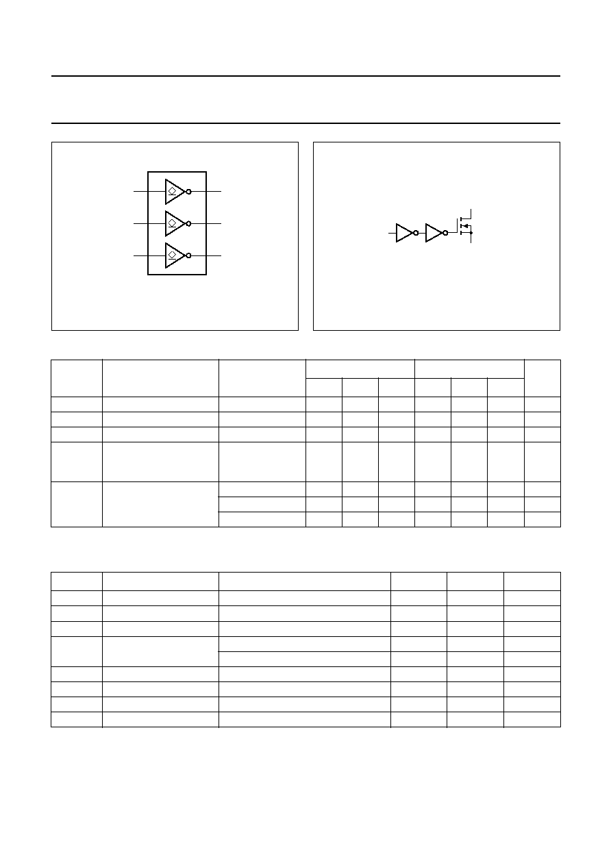
PIN
SYMBOL
DESCRIPTION
1
1A
data input
2
3Y
data output
3
2A
data input
4
GND
ground (0 V)
5
2Y
data output
6
3A
data input
7
1Y
data output
8
V
CC
supply voltage
handbook, halfpage
1
2
3
4
8
7
6
5
MNB030
06
VCC
1Y
3Y
3A
2Y
GND
2A
1A
Fig.1 Pin configuration.
handbook, halfpage
7
1
1
1
5
3
MNB031
1
2
6
Fig.2 Logic symbol.
2003 May 15
4
Philips Semiconductors
Product specification
Inverter with open-drain outputs
74HC3G06; 74HCT3G06
handbook, halfpage
MNB032
1A
1Y
1
7
2A
2Y
3
5
3A
3Y
6
2
Fig.3 IEC logic symbol.
handbook, halfpage
MNA586
Y
A
GND
Fig.4 Logic diagram (one driver).
RECOMMENDED OPERATING CONDITIONS
LIMITING VALUES
In accordance with the Absolute Maximum Rating System (IEC 60134); voltages are referenced to GND (ground = 0 V).
Notes
1. The input and output voltage ratings may be exceeded if the input and output current ratings are observed.
2. Above 110
∞
C the value of P
D
derates linearly with 8 mW/K.
SYMBOL
PARAMETER
CONDITIONS
74HC3G06
74HCT3G06
UNIT
MIN.
TYP.
MAX.
MIN.
TYP.
MAX.
V
CC
supply voltage
2.0
5.0
6.0
4.5
5.0
5.5
V
V
I
input voltage
0
-
6.0
0
-
5.5
V
V
O
output voltage
0
-
V
CC
0
-
V
CC
V
T
amb
operating ambient
temperature
see DC and AC
characteristics per
device
-
40
+25
+125
-
40
+25
+125
∞
C
t
r
, t
f
input rise and fall times
V
CC
= 2.0 V
-
-
1000
-
-
-
ns
V
CC
= 4.5 V
-
6.0
500
-
6.0
500
ns
V
CC
= 6.0 V
-
-
400
-
-
-
ns
SYMBOL
PARAMETER
CONDITIONS
MIN.
MAX.
UNIT
V
CC
supply voltage
-
0.5
+7.0
V
I
IK
input diode current
V
I
<
-
0.5 V or V
I
> V
CC
+ 0.5 V; note 1
-
±
20
mA
I
OK
output diode current
V
O
<
-
0.5 V; note 1
-
-
20
mA
V
O
output voltage
active mode; note 1
-
0.5
V
CC
+ 0.5
V
high-impedance mode; note 1
-
0.5
7.0
V
I
O
output sink current
-
0.5 V < V
O
< 7.0 V; note 1
-
-
25
mA
I
CC
, I
GND
V
CC
or GND current
note 1
-
50
mA
T
stg
storage temperature
-
65
+150
∞
C
P
D
power dissipation
T
amb
=
-
40 to +125
∞
C; note 2
-
300
mW
2003 May 15
5
Philips Semiconductors
Product specification
Inverter with open-drain outputs
74HC3G06; 74HCT3G06
DC CHARACTERISTICS
Type 74HC3G06
At recommended operating conditions; voltages are referenced to GND (ground = 0 V).
Note
1. All typical values are measured at T
amb
= 25
∞
C.
SYMBOL
PARAMETER
TEST CONDITIONS
MIN.
TYP.
MAX.
UNIT
OTHER
V
CC
(V)
T
amb
=
-
40 to +85
∞
C; note 1
V
IH
HIGH-level input voltage
2.0
1.5
1.2
-
V
4.5
3.15
2.4
-
V
6.0
4.2
3.2
-
V
V
IL
LOW-level input voltage
2.0
-
0.8
0.5
V
4.5
-
2.1
1.35
V
6.0
-
2.8
1.8
V
V
OL
LOW-level output voltage
V
I
= V
IH
or V
IL
I
O
= 20
µ
A
2.0
-
0
0.1
V
I
O
= 20
µ
A
4.5
-
0
0.1
V
I
O
= 4.0 mA
4.5
-
0.15
0.33
V
I
O
= 20
µ
A
6.0
-
0
0.1
V
I
O
= 5.2 mA
6.0
-
0.16
0.33
V
I
LI
input leakage current
V
I
= V
CC
or GND
6.0
-
-
±
1.0
µ
A
I
OZ
3-state output OFF current
V
I
= V
IH
or V
IL
;
V
O
= V
CC
or GND
6.0
-
-
±
5.0
µ
A
I
CC
quiescent supply current
V
I
= V
CC
or GND; I
O
= 0
6.0
-
-
10
µ
A
T
amb
=
-
40 to +125
∞
C
V
IH
HIGH-level input voltage
2.0
1.5
-
-
V
4.5
3.15
-
-
V
6.0
4.2
-
-
V
V
IL
LOW-level input voltage
2.0
-
-
0.5
V
4.5
-
-
1.35
V
6.0
-
-
1.8
V
V
OL
LOW-level output voltage
V
I
= V
IH
or V
IL
I
O
= 20
µ
A
2.0
-
-
0.1
V
I
O
= 20
µ
A
4.5
-
-
0.1
V
I
O
= 4.0 mA
4.5
-
-
0.4
V
I
O
= 20
µ
A
6.0
-
-
0.1
V
I
O
= 5.2 mA
6.0
-
-
0.4
V
I
LI
input leakage current
V
I
= V
CC
or GND
6.0
-
-
±
1.0
µ
A
I
OZ
3-state output OFF current
V
I
= V
IH
or V
IL
;
V
O
= V
CC
or GND
6.0
-
-
±
10
µ
A
I
CC
quiescent supply current
V
I
= V
CC
or GND; I
O
= 0
6.0
-
-
20
µ
A
