1999 Oct 01
2
Philips Semiconductors
Product specification
Octal D-type flip-flop with reset; positive
edge-trigger; open drain outputs
74HCT7273
FEATURES
∑
ESD protection:
HBM EIA/JESD22-A114-A
Exceeds 2000 V
MM EIA/JESD22-A115-A
Exceeds 200 V
∑
Ideal buffer for MOS
microprocessor or memory
∑
Eight positive edge-triggered
D-type flip-flops
∑
Common clock and master reset
∑
Output capability: standard (open
drain)
∑
I
CC
category: MSI.
DESCRIPTION
The 74HCT7273 is a high-speed SI-gate CMOS device and is pin compatible
with Low power Schottky TTL (LSTTL). It is specified in compliance with
JEDEC standard no 7A.
The 74HCT7273 has eight edge-triggered D-type flip-flops with individual D
inputs and Q outputs. The common Clock (CP) and Master Reset (MR) inputs
load and reset (clear) all flip-flops simultaneously.
The state of each D input, one set-up time before the LOW-to-HIGH clock
transition, is transferred to the corresponding output (Q
n
) of the flip-flop.
A LOW level on the MR input forces all outputs LOW, independently of the clock
or data inputs.
The device is useful for applications requiring true outputs only and clock and
master reset inputs that are common to all storage elements.
The 74HCT7273 has open-drain N-outputs, which are clamped by a diode
connected to V
CC
. When a HIGH is clocked in the flip-flop, the output comes in
the high-impedance OFF-state. The output may now be pulled to any voltage
between GND and V
Omax
. This allows the device to be used as a LOW-to-HIGH
or HIGH-to-LOW level shifter. For digital operation and OR-tied output
applications, the device must have a pull-up resistor to establish a logic HIGH
level.
QUICK REFERENCE DATA
Ground = 0 V; T
amb
= 25
∞
C; t
r
= t
f
= 6.0 ns.
Notes
1. C
PD
is used to determine the dynamic power dissipation (P
D
in
µ
W).
P
D
= C
PD
◊
V
CC
2
◊
f
i
+
(C
L
◊
V
CC
2
◊
f
o
) +
(V
0
2
/R
L
)
◊
duty factor LOW where:
f
i
= input frequency in MHz;
f
o
= output frequency in MHz;
(C
L
◊
V
CC
2
◊
f
o
) = sum of outputs;
C
L
= output load capacitance in pF;
R
L
= pull-up resistor in M
;
V
CC
= supply voltage in Volts.
2. The condition is V
I
= GND to V
CC
-
1.5 V.
SYMBOL
PARAMETER
CONDITIONS
TYPICAL
UNIT
t
PZL
/t
PLZ
propagation delay
C
L
= 50 pF; V
CC
= 4.5 V
CP to Q
n
16
ns
MR to Q
n
23
ns
f
max
maximum clock frequency
56
MHz
C
I
input capacitance
3.5
pF
C
PD
power dissipation capacitance
C
L
= 50 pF; f = 1 MHz; notes 1 and 2
37
pF
1999 Oct 01
3
Philips Semiconductors
Product specification
Octal D-type flip-flop with reset; positive
edge-trigger; open drain outputs
74HCT7273
FUNCTION TABLE
See note 1.
Note
1. H = HIGH voltage level;
h = HIGH voltage level one set-up time prior to the LOW-to-HIGH CP transition;
L = LOW voltage level.
l = LOW voltage level one set-up time prior to the LOW-to-HIGH CP transition;
Z = high-impedance OFF-state;
X = don't care;
= LOW-to-HIGH CP transition.
ORDERING INFORMATION
OPERATING MODES
INPUTS
OUTPUTS
MR
CP
D
n
Q
n
Reset (clear)
L
X
X
L
Load `1'
H
h
Z
Load `0'
H
l
L
OUTSIDE NORTH
AMERICA
NORTH AMERICA
PACKAGE
TEMPERATURE
RANGE
PINS
PACKAGE
MATERIAL
CODE
74HCT7273D
74HCT7273D
-
40 to +125
∞
C
20
SO
plastic
SOT163-1
74HCT7273N
74HCT7273N
20
DIP
plastic
SOT146-1

1999 Oct 01
4
Philips Semiconductors
Product specification
Octal D-type flip-flop with reset; positive
edge-trigger; open drain outputs
74HCT7273
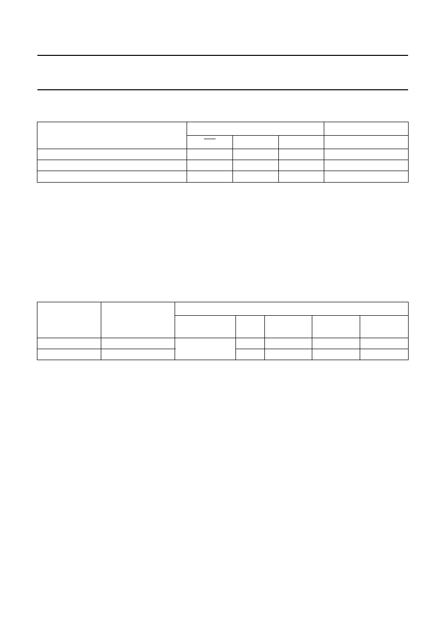
PINNING
PIN
SYMBOL
DESCRIPTION
1
MR
asynchronous master reset (active LOW)
2, 5, 6, 9, 12, 15, 16, 19
Q
0
to Q
7
flip-flop outputs
3, 4, 7, 8, 13, 14, 17, 18
D
0
to D
7
data inputs
10
GND
ground (0 V)
11
CP
clock input (LOW-to-HIGH, edge triggered)
20
V
CC
DC supply voltage
Fig.1 Pin configuration.
handbook, halfpage
MR
Q0
D0
D1
Q1
Q2
D2
D3
Q3
GND
VCC
Q7
D7
D6
Q5
D5
Q6
D4
Q4
CP
1
2
3
4
5
6
7
8
9
10
11
12
20
19
18
17
16
15
14
13
7273
MNA380
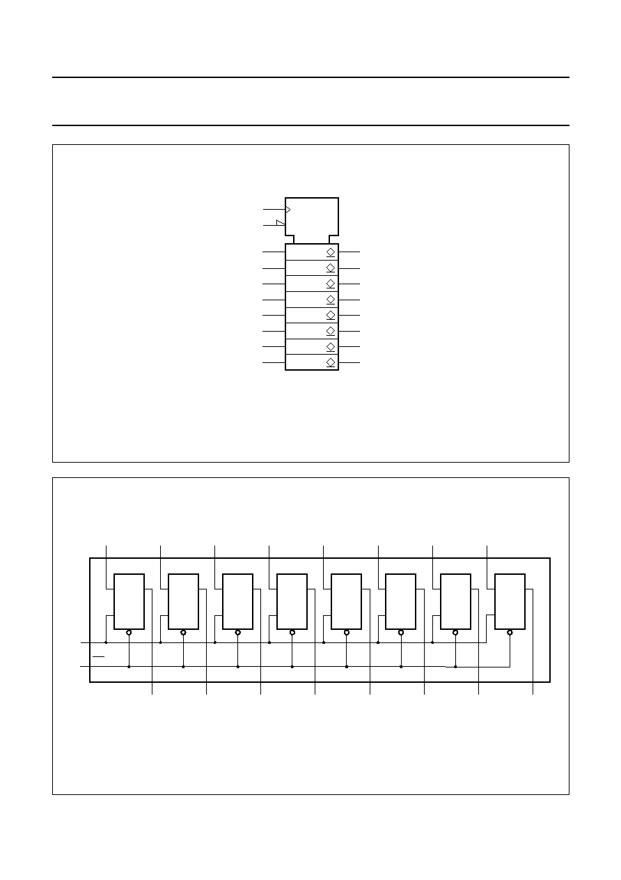
Fig.2 Logic symbol.
handbook, halfpage
MNA381
D0 D1 D2 D3 D4 D5 D6 D7
CP
Q0 Q1 Q2 Q3 Q4 Q5 Q6 Q7
11
1
19
16
15
12
9
6
5
2
18
17
14
13
8
7
4
3
MR