 | –≠–ª–µ–∫—Ç—Ä–æ–Ω–Ω—ã–π –∫–æ–º–ø–æ–Ω–µ–Ω—Ç: 74LV157N | –°–∫–∞—á–∞—Ç—å:  PDF PDF  ZIP ZIP |
Document Outline
- FEATURES
- DESCRIPTION
- QUICK REFERENCE DATA
- ORDERING INFORMATION
- PIN CONFIGURATION
- LOGIC SYMBOL
- PIN DESCRIPTION
- FUNCTIONAL DIAGRAM
- LOGIC SYMBOL (IEEE/IEC)
- RECOMMENDED OPERATING CONDITIONS
- ABSOLUTE MAXIMUM RATINGS
- DC ELECTRICAL CHARACTERISTICS
- AC CHARACTERISTICS
- AC WAVEFORMS
- TEST CIRCUIT
- PACKAGE OUTLINES
- SOT38-4
- SOT109-1
- SOT338-1
- SOT403-1
- DEFINITIONS
Philips
Semiconductors
74LV157
Quad 2-input multiplexer
Product specification
Supersedes data of 1997 May 15
IC24 Data Handbook
1998 Apr 30
INTEGRATED CIRCUITS

Philips Semiconductors
Product specification
74LV157
Quad 2-input multiplexer
2
1998 Apr 30
853≠1920 19318
FEATURES
∑
Optimized for low voltage applications: 1.0 to 3.6 V
∑
Accepts TTL input levels between V
CC
= 2.7 V and V
CC
= 3.6 V
∑
Typical V
OLP
(output ground bounce) < 0.8 V at V
CC
= 3.3 V,
T
amb
= 25
∞
C
∑
Typical V
OHV
(output V
OH
undershoot) > 2 V at V
CC
= 3.3 V,
T
amb
= 25
∞
C
∑
Output capability: standard
∑
I
CC
category: MSI
DESCRIPTION
The 74LV157 is a low-voltage CMOS device and is pin and function
compatible with 74HC/HCT157.
The 74LV157 is a quad 2-input multiplexer which selects 4 bits of data
from two sources under the control of a common data select input (S).
The four outputs present the selected data in the true (non-inverted)
form. The enable input (E) is active LOW. When E is HIGH, all of the
outputs (1Y to 4Y) are forced LOW regardless of all other input
conditions.
Moving the data from two groups of registers to four common output
buses is a common use of the 74LV157. The state of the common
data select input (S) determines the particular register from which
the data comes. It can also be used as function generator.
The device is useful for implementing highly irregular logic by
generating any four of the 16 different functions of two variables with
one variable common.
The 74LV157 is the logic implementation of a 4-pole, 2-position
switch, where the position of the switch is determined by the logic
levels applied to S.
QUICK REFERENCE DATA
GND = 0 V; T
amb
= 25
∞
C; t
r
= t
f
2.5 ns
SYMBOL
PARAMETER
CONDITIONS
TYPICAL
UNIT
t
PHL
/t
PLH
Propagation delay
nl
0
, nl
1
, to nY
E to nY
S to nY
C
L
= 15 pF;
V
CC
= 3.3 V
10
11
12
ns
C
I
Input capacitance
3.5
pF
C
PD
Power dissipation capacitance per gate
V
I
= GND to V
CC
1
70
pF
NOTES:
1. C
PD
is used to determine the dynamic power dissipation (P
D
in
µ
W)
P
D
= C
PD
◊
V
CC
2
◊
f
i
)
(C
L
◊
V
CC
2
◊
f
o
) where:
f
i
= input frequency in MHz; C
L
= output load capacitance in pF;
f
o
= output frequency in MHz; V
CC
= supply voltage in V;
(C
L
◊
V
CC
2
◊
f
o
) = sum of the outputs.
ORDERING INFORMATION
PACKAGES
TEMPERATURE RANGE
OUTSIDE NORTH AMERICA
NORTH AMERICA
PKG. DWG. #
16-Pin Plastic DIL
≠40
∞
C to +125
∞
C
74LV157 N
74LV157 N
SOT38-4
16-Pin Plastic SO
≠40
∞
C to +125
∞
C
74LV157 D
74LV157 D
SOT109-1
16-Pin Plastic SSOP Type II
≠40
∞
C to +125
∞
C
74LV157 DB
74LV157 DB
SOT338-1
16-Pin Plastic TSSOP Type I
≠40
∞
C to +125
∞
C
74LV157 PW
74LV157PW DH
SOT403-1

Philips Semiconductors
Product specification
74LV157
Quad 2-input multiplexer
1998 Apr 30
3
PIN CONFIGURATION
SV00563
1
2
3
4
5
6
S
1I
0
1I
1
1Y
2I
0
2I
1
V
CC
E
4I
0
4I
1
4Y
3I
0
16
15
14
13
12
11
7
8
2Y
GND
3I
1
3Y
10
9
PIN DESCRIPTION
PIN
NUMBER
SYMBOL
FUNCTION
1
S
Common data select input
2, 5, 11, 14
1l
0
to 4l
0
Data inputs from source 0
3, 6, 10, 13
1l
1
to 4l
1
Data inputs from source 1
4, 7, 9, 12
1Y to 4Y
Multiplexer outputs
8
GND
Ground (0 V)
15
E
Enable inputs (active LOW)
16
V
CC
Positive supply voltage
LOGIC SYMBOL (IEEE/IEC)
SV00565
EN
G1
15
1
7
4
9
12
6
5
3
2
MUX
1
11
10
14
13
1
LOGIC SYMBOL
SV00564
1
S
E
2
1I0
2I0
3I0
4I0
1I1
2I1
3I1
4I1
3
5
4
1Y
6
7
2Y
10
12
4Y
14
11
9
3Y
13
15
FUNCTIONAL DIAGRAM
SV00566
E
S
SELECTOR
MULTIPLEXER
OUTPUTS
1I 0
1Y
2Y
3Y
4Y
1I 1
2I 0
2I 1
3I 0
3I 1
4I 0
4I 1
1
15
7
4
9
12
6
5
2
3
11
10
14
13

Philips Semiconductors
Product specification
74LV157
Quad 2-input multiplexer
1998 Apr 30
4
RECOMMENDED OPERATING CONDITIONS
SYMBOL
PARAMETER
CONDITIONS
MIN
TYP
MAX
UNIT
V
CC
DC supply voltage
See Note 1
1.0
3.3
3.6
V
V
I
Input voltage
0
≠
V
CC
V
V
O
Output voltage
0
≠
V
CC
V
T
amb
Operating ambient temperature range in free air
See DC and AC
characteristics
≠40
≠40
+85
+125
∞
C
t
r
, t
f
Input rise and fall times
V
CC
= 1.0V to 2.0V
V
CC
= 2.0V to 2.7V
V
CC
= 2.7V to 3.6V
≠
≠
≠
≠
≠
≠
500
200
100
ns/V
NOTE:
1. The LV is guaranteed to function down to V
CC
= 1.0V (input levels GND or V
CC
); DC characteristics are guaranteed from V
CC
= 1.2V to V
CC
= 3.6V.
ABSOLUTE MAXIMUM RATINGS
1, 2
In accordance with the Absolute Maximum Rating System (IEC 134).
Voltages are referenced to GND (ground = 0 V).
SYMBOL
PARAMETER
CONDITIONS
RATING
UNIT
V
CC
DC supply voltage
≠0.5 to +4.6
V
"
I
IK
DC input diode current
V
I
< ≠0.5 or V
I
> V
CC
+ 0.5V
20
mA
"
I
OK
DC output diode current
V
O
< ≠0.5 or V
O
> V
CC
+ 0.5V
50
mA
"
I
O
DC output source or sink current
≠ standard outputs
≠0.5V < V
O
< V
CC
+ 0.5V
25
mA
"
I
GND
,
"
I
CC
DC V
CC
or GND current for types with
≠ standard outputs
50
mA
T
stg
Storage temperature range
≠65 to +150
∞
C
P
TOT
Power dissipation per package
≠ plastic DIL
≠ plastic mini-pack (SO)
≠ plastic shrink mini-pack (SSOP and TSSOP)
for temperature range: ≠40 to +125
∞
C
above +70
∞
C derate linearly with 12 mW/K
above +70
∞
C derate linearly with 8 mW/K
above +60
∞
C derate linearly with 5.5 mW/K
750
500
400
mW
NOTES:
1. Stresses beyond those listed may cause permanent damage to the device. These are stress ratings only and functional operation of the
device at these or any other conditions beyond those indicated under "recommended operating conditions" is not implied. Exposure to
absolute-maximum-rated conditions for extended periods may affect device reliability.
2. The input and output voltage ratings may be exceeded if the input and output current ratings are observed.
Philips Semiconductors
Product specification
74LV157
Quad 2-input multiplexer
1998 Apr 30
5
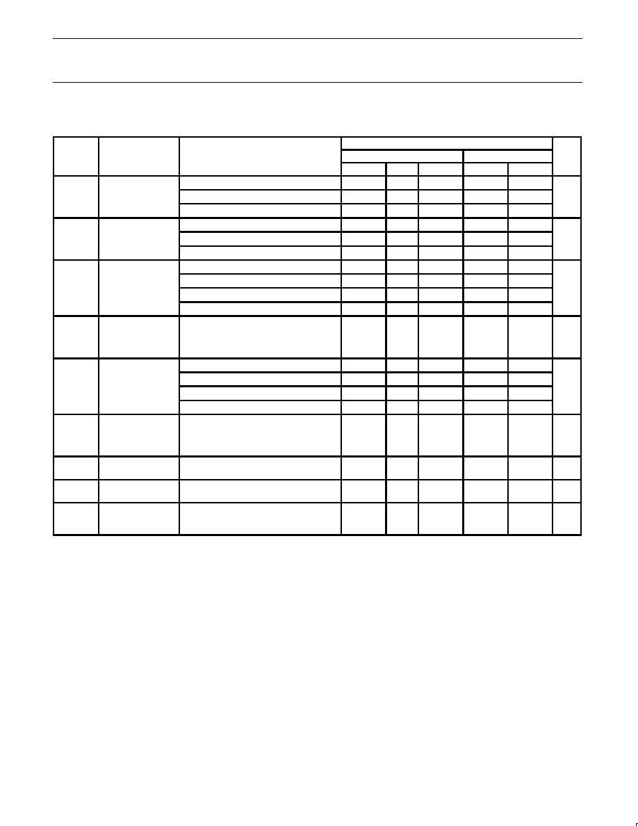
DC ELECTRICAL CHARACTERISTICS
Over recommended operating conditions. Voltages are referenced to GND (ground = 0 V).
LIMITS
SYMBOL
PARAMETER
TEST CONDITIONS
-40
∞
C to +85
∞
C
-40
∞
C to +125
∞
C
UNIT
MIN
TYP
1
MAX
MIN
MAX
HIGH l
l I
t
V
CC
= 1.2 V
0.9
0.9
V
IH
HIGH level Input
voltage
V
CC
= 2.0 V
1.4
1.4
V
voltage
V
CC
= 2.7 to 3.6 V
2.0
2.0
LOW l
l I
t
V
CC
= 1.2 V
0.3
0.3
V
IL
LOW level Input
voltage
V
CC
= 2.0 V
0.6
0.6
V
voltage
V
CC
= 2.7 to 3.6 V
0.8
0.8
V
CC
= 1.2 V; V
I
= V
IH
or V
IL;
≠I
O
= 100
µ
A
1.2
V
O
HIGH level output
V
CC
= 2.0 V; V
I
= V
IH
or V
IL;
≠I
O
= 100
µ
A
1.8
2.0
1.8
V
V
OH
voltage; all outputs
V
CC
= 2.7 V; V
I
= V
IH
or V
IL;
≠I
O
= 100
µ
A
2.5
2.7
2.5
V
V
CC
= 3.0 V; V
I
= V
IH
or V
IL;
≠I
O
= 100
µ
A
2.8
3.0
2.8
V
OH
HIGH level output
voltage;
STANDARD
outputs
V
CC
= 3.0 V; V
I
= V
IH
or V
IL;
≠I
O
= 6mA
2.40
2.82
2.20
V
V
CC
= 1.2 V; V
I
= V
IH
or V
IL;
I
O
= 100
µ
A
0
V
O
LOW level output
V
CC
= 2.0 V; V
I
= V
IH
or V
IL;
I
O
= 100
µ
A
0
0.2
0.2
V
V
OL
voltage; all outputs
V
CC
= 2.7 V; V
I
= V
IH
or V
IL;
I
O
= 100
µ
A
0
0.2
0.2
V
V
CC
= 3.0 V; V
I
= V
IH
or V
IL;
I
O
= 100
µ
A
0
0.2
0.2
V
OL
LOW level output
voltage;
STANDARD
outputs
V
CC
= 3.0 V; V
I
= V
IH
or V
IL;
I
O
= 6mA
0.25
0.40
0.50
V
I
I
Input leakage
current
V
CC
= 3.6 V; V
I
= V
CC
or GND
1.0
1.0
µ
A
I
CC
Quiescent supply
current; MSI
V
CC
= 3.6 V; V
I
= V
CC
or GND; I
O
= 0
20.0
160
µ
A
I
CC
Additional
quiescent supply
current per input
V
CC
= 2.7 V to 3.6 V; V
I
= V
CC
≠ 0.6 V
500
850
µ
A
NOTE:
1. All typical values are measured at T
amb
= 25
∞
C.