Philips Semiconductors
Product specification
74LV163
Presettable synchronous 4-bit binary counter;
synchronous reset
2
1998 Apr 30
8531916 19318
FEATURES
·
Optimized for low voltage applications: 1.0 to 3.6 V
·
Accepts TTL input levels between V
CC
= 2.7 V and V
CC
= 3.6 V
·
Typical V
OLP
(output ground bounce) < 0.8 V at V
CC
= 3.3 V,
T
amb
= 25
°
C
·
Typical V
OHV
(output V
OH
undershoot) > 2 V at V
CC
= 3.3 V,
T
amb
= 25
°
C
·
Synchronous counting and loading
·
Two count enable inputs for n-bit cascading
·
Positive-edge triggered clock
·
Synchronous reset
·
Output capability: standard
·
I
CC
category: MSI
DESCRIPTION
The 74LV163 is a low-voltage Si-gate CMOS device and is pin and
function compatible with 74HC/HCT163.
The 74LV163 is a synchronous presettable binary counter which
features an internal look-head carry and can be used for high-speed
counting. Synchronous operation is provided by having all flip-flops
clocked simultaneously on the positive-going edge of the clock (CP).
The outputs (Q
0
to Q
3
) of the counters may be preset to a HIGH or
LOW level. A LOW level at the parallel enable input (PE) disables the
counting action and causes the data at the data inputs (D
0
to D
3
) to be
loaded into the counter on the positive-going edge of the clock
(providing that the set-up and hold time requirements for PE are met).
Preset takes place regardless of the levels at count enable inputs
(CEP and CET). A low level at the master reset input (MR) sets all
four outputs of the flip-flops (Q
0
to Q
3
) to LOW level after the next
positive-going transition on the clock (CP) input (provided that the
set-up and hold time requirements for MR are met).
This action occurs regardless of the levels at PE, CET and CEP
inputs. This synchronous reset feature enables the designer to
modify the maximum count with only one external NAND gate. The
look ahead carry simplifies serial cascading of the counters. Both
count enable inputs (CEP and CET) must be HIGH to count. The
CET input is fed forward to enable the terminal count output (TC).
The TC output thus enabled will produce a HIGH output pulse of a
duration approximately equal to a HIGH level output of Q
0
. This
pulse can be used to enable the next cascading stage. The
maximum clock frequency for the cascaded counters is determined
by the CP to TC propagation delay and CEP to CP set-up time,
according to the following formula:
f
max
+
1
tp
(max)
(CP to TC)
)
t
su
(CEP to CP)
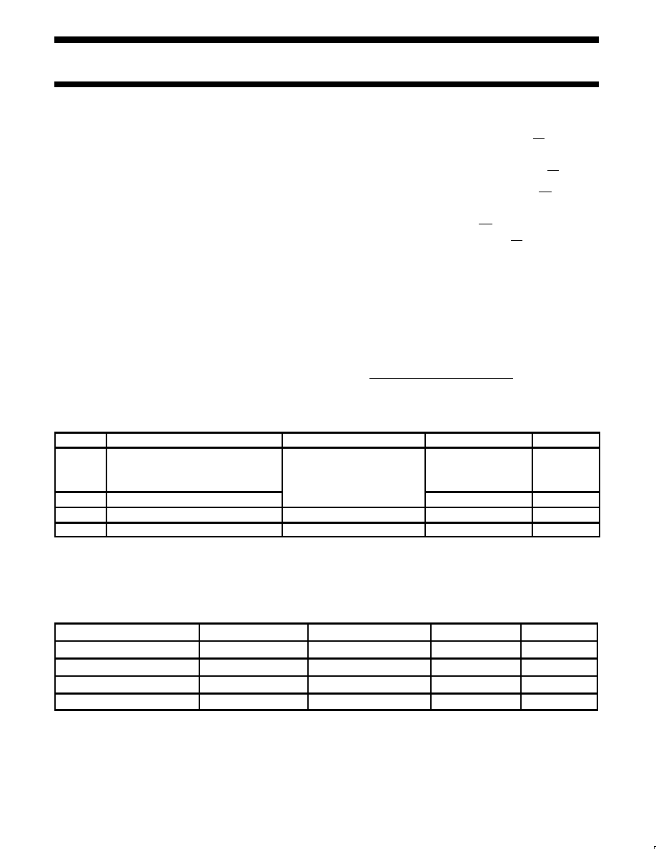
QUICK REFERENCE DATA
GND = 0 V; T
amb
= 25
°
C; t
r
= t
f
2.5 ns
SYMBOL
PARAMETER
CONDITIONS
TYPICAL
UNIT
t
PHL
/t
PLH
Propagation delay
CP to Q
n
CP to TC
CET to TC
C
L
= 15 pF;
V
CC
= 3.3 V
15
18
9
ns
f
max
Maximum clock frequency
77
MHz
C
I
Input capacitance
3.5
pF
C
PD
Power dissipation capacitance per gate
V
I
= GND to V
CC
1
25
pF
NOTES:
1. C
PD
is used to determine the dynamic power dissipation (P
D
in
µ
W)
P
D
= C
PD
×
V
CC
2
×
f
i
)
(C
L
×
V
CC
2
×
f
o
) where:
f
i
= input frequency in MHz; C
L
= output load capacitance in pF;
f
o
= output frequency in MHz; V
CC
= supply voltage in V;
(C
L
×
V
CC
2
×
f
o
) = sum of the outputs.
ORDERING INFORMATION
PACKAGES
TEMPERATURE RANGE
OUTSIDE NORTH AMERICA
NORTH AMERICA
PKG. DWG. #
16-Pin Plastic DIL
40
°
C to +125
°
C
74LV163 N
74LV163 N
SOT38-4
16-Pin Plastic SO
40
°
C to +125
°
C
74LV163 D
74LV163 D
SOT109-1
16-Pin Plastic SSOP Type II
40
°
C to +125
°
C
74LV163 DB
74LV163 DB
SOT338-1
16-Pin Plastic TSSOP Type I
40
°
C to +125
°
C
74LV163 PW
74LV163PW DH
SOT403-1
Philips Semiconductors
Product specification
74LV163
Presettable synchronous 4-bit binary counter;
synchronous reset
1998 Apr 30
3
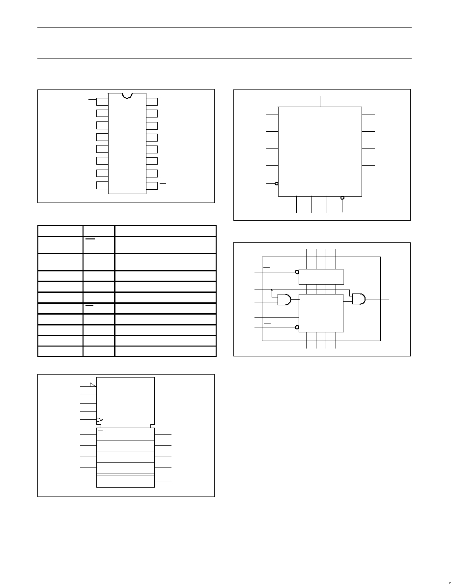
PIN CONFIGURATION
SV00569
1
2
3
4
5
6
MR
CP
D
0
D
1
D
2
D
3
V
CC
TC
Q
0
16
15
14
13
12
11
7
8
GND
CET
PE
10
9
CEP
Q
1
Q
2
Q
3
PIN DESCRIPTION
PIN NUMBER
SYMBOL
FUNCTION
1
MR
Asynchronous master reset
(active LOW)
2
CP
Clock input
(LOW-to-HIGH, edge-triggered)
3, 4, 5, 6
D
0
to D
3
Data inputs
7
CEP
Count enable inputs
8
GND
Ground (0 V)
9
PE
Parallel enable input (active LOW)
10
CET
Count enable carry input
14, 13, 12, 11
Q
0
to Q
3
Flip-flop outputs
15
TC
Terminal count output
16
V
CC
Positive supply voltage
LOGIC SYMBOL (IEEE/IEC)
SV00571
CTR4
4CT = 15
1, 2D
M1
R
G3
G4
1
10
7
9
2
3
4
5
6
15
11
12
13
14
C2/1,3,4+
LOGIC SYMBOL
SV00570
14
13
12
11
15
Q
0
Q
1
Q
2
Q
3
MR
CP
CET
CEP
PE
D
3
D
2
D
1
D
0
TC
9
2
10
7
1
6
5
4
3
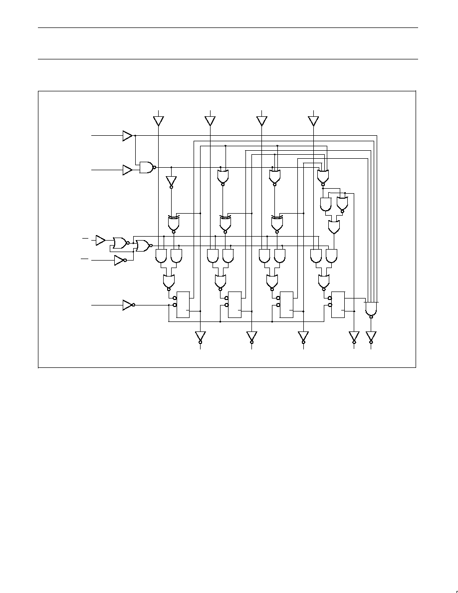
FUNCTIONAL DIAGRAM
SV00572
PE
CP
TC
CET
CEP
MR
7
10
15
2
1
9
D
3
Q
3
D
2
Q
2
D
1
Q
1
D
0
Q
0
BINARY
COUNTER
PARALLEL LOAD
CIRCUITRY
6
11
5
12
4
13
3
14
Philips Semiconductors
Product specification
74LV163
Presettable synchronous 4-bit binary counter;
synchronous reset
1998 Apr 30
4
FUNCTION TABLE
OPERATING MODES
INPUTS
OUTPUTS
OPERATING MODES
MR
CP
CEP
CET
PE
D
n
Q
n
TC
Reset (clear)
l
X
X
X
X
L
L
Parallel load
h
X
X
I
I
L
L
Parallel load
h
X
X
I
h
H
*
Count
h
h
h
h
X
Count
*
Hold (do nothing)
h
X
I
X
h
X
q
n
*
Hold (do nothing)
h
X
X
I
h
X
q
n
L
NOTES:
*
=
The TC output is HIGH when CET is HIGH and the counter is at terminal count (HHHH)
H =
HIGH voltage level
h
=
HIGH voltage level one set-up time prior to the LOW-to-HIGH clock transition
L
=
LOW voltage level
I
=
LOW voltage level level one set-up time prior to the LOW-to-HIGH clock transition
q
=
lower case letters indicate the state of the referenced output one set-up time prior to the LOW-to-HIGH clock transition
X =
don't care
=
LOW-to-HIGH clock transition
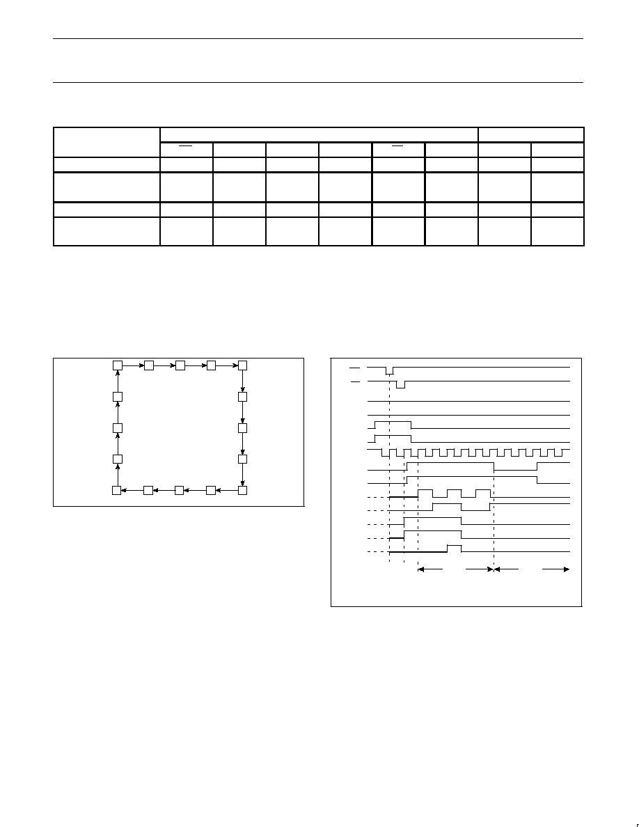
STATE DIAGRAM
SV00573
0
1
2
3
4
5
6
7
8
9
10
11
12
15
14
13
TYPICAL TIMING SEQUENCE
SV00582
MR
PE
D
0
D
1
D
2
D
3
CP
CEP
CET
Q
0
Q
1
Q
2
Q
3
TC
reset preset
count
inhibit
13
14
15
0
1
2
12
Typical timing sequence: reset outputs to zero; preset to binary twelve; count to
thirteen, fourteen, fifteen, zero, one and two; inhibit