 | ÐлекÑÑоннÑй компоненÑ: 74LV368D | СкаÑаÑÑ:  PDF PDF  ZIP ZIP |
Äîêóìåíòàöèÿ è îïèñàíèÿ www.docs.chipfind.ru
Philips
Semiconductors
74LV368
Hex buffer/line driver; inverting (3-State)
Product specification
Supersedes data of 1997 Apr 07
IC24 Data Handbook
1998 May 29
INTEGRATED CIRCUITS
Philips Semiconductors
Product specification
74LV368
Hex buffer/line driver; inverting (3-State)
2
1998 May 29
8531966 19466
FEATURES
·
Optimized for Low Voltage applications: 1.0 to 3.6V
·
Accepts TTL input levels between V
CC
= 2.7V and V
CC
= 3.6V
·
Typical V
OLP
(output ground bounce)
t
0.8V @ V
CC
= 3.3V,
T
amb
= 25
°
C
·
Typical V
OHV
(output V
OH
undershoot)
u
2V @ V
CC
= 3.3V,
T
amb
= 25
°
C
·
Inverting outputs
·
Output capability: bus driver
·
I
CC
category: SSI
DESCRIPTION
The 74LV368 a lowvoltage Sigate CMOS device and is pin and
function compatible with 74HC/HCT368.
The 74LV368 is a hex inverting buffer/line driver with 3state
outputs. The 3state outputs (nY) are controlled by the output
enable inputs 1OE and 2OE. A HIGH on nOE causes the outputs to
assume a high impedance OFFstate.
QUICK REFERENCE DATA
GND = 0V; T
amb
= 25
°
C; t
r
=t
f
v
2.5 ns
SYMBOL
PARAMETER
CONDITIONS
TYPICAL
UNIT
t
PHL
/t
PLH
Propagation delay
nA to nY
C
L
= 15pF
V
CC
= 3.3V
9.0
ns
C
I
Input capacitance
3.5
pF
C
PD
Power dissipation capacitance per buffer
Notes 1, 2
30
pF
NOTES:
1
C
PD
is used to determine the dynamic power dissipation (P
D
in
µ
W)
P
D
= C
PD
V
CC
2
x f
i
)S
(C
L
V
CC
2
f
o
) where:
f
i
= input frequency in MHz; C
L
= output load capacitance in pF;
f
o
= output frequency in MHz; V
CC
= supply voltage in V;
S
(C
L
V
CC
2
f
o
) = sum of the outputs.
2
The condition is V
I
= GND to V
CC
ORDERING INFORMATION
PACKAGES
TEMPERATURE RANGE
OUTSIDE NORTH AMERICA
NORTH AMERICA
PKG. DWG. #
16-Pin Plastic DIL
40
°
C to +125
°
C
74LV368 N
74LV368 N
SOT38-4
16-Pin Plastic SO
40
°
C to +125
°
C
74LV368 D
74LV368 D
SOT109-1
16-Pin Plastic SSOP Type II
40
°
C to +125
°
C
74LV368 DB
74LV368 DB
SOT338-1
16-Pin Plastic TSSOP Type I
40
°
C to +125
°
C
74LV368 PW
74LV368PW DH
SOT403-1
Philips Semiconductors
Product specification
74LV368
Hex buffer/line driver; inverting (3-State)
1998 May 29
3
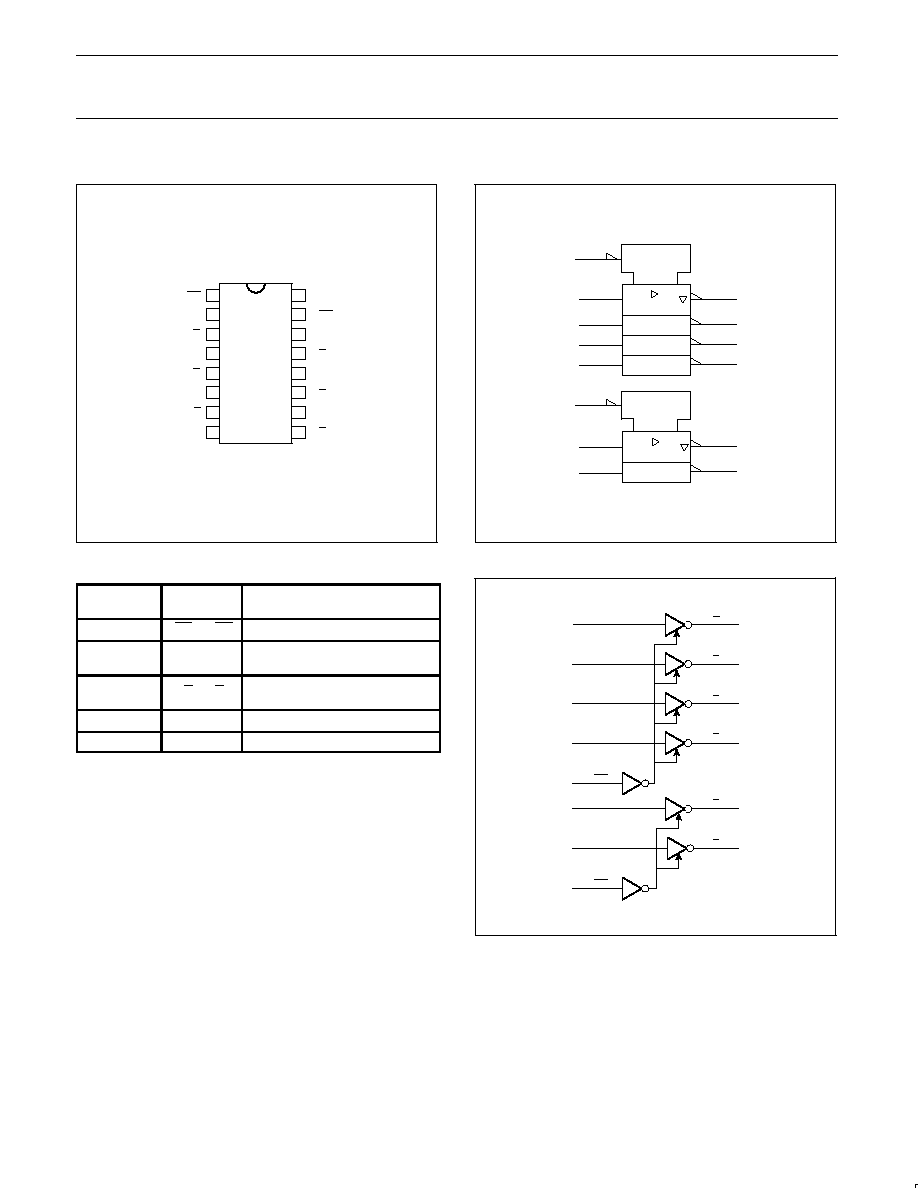
PIN CONFIGURATION
8
7
1
2
3
4
5
6
9
10
11
12
13
14
15
16
1OE
1A
1Y
2A
2Y
3A
3Y
GND
4Y
5A
4A
6Y
6A
2OE
V
CC
5Y
SV00373
PIN DESCRIPTION
PIN
NUMBER
SYMBOL
FUNCTION
1, 15
1OE to 2OE
Output enable inputs (active LOW)
2, 4, 6, 10,
12, 14
1A to 6A
Data inputs
3, 5, 7,
9, 11, 13
1Y to 6Y
Bus outputs
8
GND
Ground (0V)
16
V
CC
Positive supply voltage
LOGIC SYMBOL (IEEE/IEC)
1
2
4
6
10
12
14
15
3
5
7
9
11
13
EN
EN
SV00374
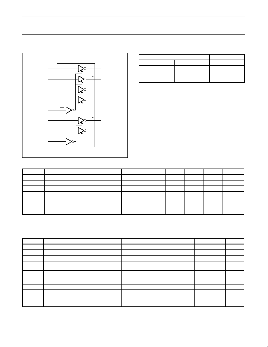
LOGIC SYMBOL
2
4
6
10
1
12
14
15
3
5
7
9
11
13
1A
2A
3A
4A
1OE
5A
6A
2OE
1Y
2Y
3Y
4Y
5Y
6Y
SV00375
Philips Semiconductors
Product specification
74LV368
Hex buffer/line driver; inverting (3-State)
1998 May 29
4
FUNCTIONAL DIAGRAM
2
3
1A
1Y
4
5
2A
2Y
6
7
3A
3Y
10
9
4A
4Y
12
11
5A
5Y
14
13
6A
6Y
1
1OE
15
2OE
SV00376
FUNCTION TABLE
INPUTS
OUTPUT
nOE
nA
nY
L
L
H
L
H
L
H
X
Z
NOTES:
H = HIGH voltage level
L = LOW voltage level
X = Don't care
Z = High impedance OFF-state
RECOMMENDED OPERATING CONDITIONS
SYMBOL
PARAMETER
CONDITIONS
MIN
TYP.
MAX
UNIT
V
CC
DC supply voltage
See Note
1
1.0
3.3
3.6
V
V
I
Input voltage
0
V
CC
V
V
O
Output voltage
0
V
CC
V
T
amb
Operating ambient temperature range
in free air
See DC and AC
characteristics
40
40
+85
+125
°
C
t
r
, t
f
Input rise and fall times
V
CC
= 1.0V to 2.0V
V
CC
= 2.0V to 2.7V
V
CC
= 2.7V to 3.6V
500
200
100
ns/V
NOTES:
1
The LV is guaranteed to function down to V
CC
= 1.0V (input levels GND or V
CC
); DC characteristics are guaranteed from V
CC
= 1.2V to V
CC
= 3.6V.
ABSOLUTE MAXIMUM RATINGS
1, 2
In accordance with the Absolute Maximum Rating System (IEC 134); Voltages are referenced to GND (ground = 0V)
SYMBOL
PARAMETER
CONDITIONS
RATING
UNIT
V
CC
DC supply voltage
0.5 to +4.6
V
±
I
IK
DC input diode current
V
I
< 0.5 or V
I
> V
CC
+ 0.5V
20
mA
±
I
OK
DC output diode current
V
O
< 0.5 or V
O
> V
CC
+ 0.5V
50
mA
±
I
O
DC output source or sink current
bus driver outputs
0.5V < V
O
< V
CC
+ 0.5V
35
mA
±
I
GND
,
±
I
CC
DC V
CC
or GND current for types with
bus driver outputs
70
mA
T
stg
Storage temperature range
65 to +150
°
C
P
TOT
Power dissipation per package
plastic DIL
plastic mini-pack (SO)
plastic shrink mini-pack (SSOP and TSSOP)
for temperature range: 40 to +125
°
C
above +70
°
C derate linearly with 12mW/K
above +70
°
C derate linearly with 8 mW/K
above +60
°
C derate linearly with 5.5 mW/K
750
500
400
mW
NOTES:
1
Stresses beyond those listed may cause permanent damage to the device. These are stress ratings only and functional operation of the
device at these or any other conditions beyond those indicated under "recommended operating conditions" is not implied. Exposure to
absolute-maximum-rated conditions for extended periods may affect device reliability.
2
The input and output voltage ratings may be exceeded if the input and output current ratings are observed.
Philips Semiconductors
Product specification
74LV368
Hex buffer/line driver; inverting (3-State)
1998 May 29
5
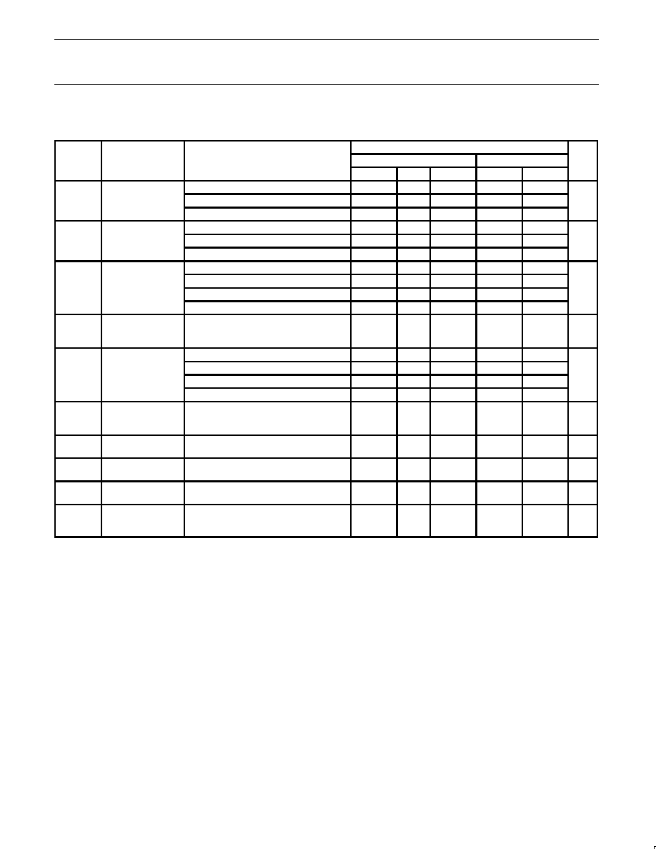
DC CHARACTERISTICS FOR THE LV FAMILY
Over recommended operating conditions voltages are referenced to GND (ground = 0V)
LIMITS
SYMBOL
PARAMETER
TEST CONDITIONS
-40
°
C to +85
°
C
-40
°
C to +125
°
C
UNIT
MIN
TYP
1
MAX
MIN
MAX
HIGH level Input
V
CC
= 1.2V
0.9
0.9
V
IH
HIGH level Input
voltage
V
CC
= 2.0V
1.4
1.4
V
voltage
V
CC
= 2.7 to 3.6V
2.0
2.0
LOW level Input
V
CC
= 1.2V
0.3
0.3
V
IL
LOW level Input
voltage
V
CC
= 2.0V
0.6
0.6
V
voltage
V
CC
= 2.7 to 3.6V
0.8
0.8
V
CC
= 1.2V; V
I
= V
IH
or V
IL;
I
O
= 100
µ
A
1.2
V
OH
HIGH level output
V
CC
= 2.0V; V
I
= V
IH
or V
IL;
I
O
= 100
µ
A
1.8
2.0
1.8
V
V
OH
voltage; all outputs
V
CC
= 2.7V; V
I
= V
IH
or V
IL;
I
O
= 100
µ
A
2.5
2.7
2.5
V
V
CC
= 3.0V; V
I
= V
IH
or V
IL;
I
O
= 100
µ
A
2.8
3.0
2.8
V
OH
HIGH level output
voltage; BUS driver
outputs
V
CC
= 3.0V;V
I
= V
IH
or V
IL;
I
O
= 8mA
2.40
2.82
2.20
V
V
CC
= 1.2V; V
I
= V
IH
or V
IL;
I
O
= 100
µ
A
0
V
OL
LOW level output
V
CC
= 2.0V; V
I
= V
IH
or V
IL;
I
O
= 100
µ
A
0
0.2
0.2
V
V
OL
voltage; all outputs
V
CC
= 2.7V; V
I
= V
IH
or V
IL;
I
O
= 100
µ
A
0
0.2
0.2
V
V
CC
= 3.0V;V
I
= V
IH
or V
IL;
I
O
= 100
µ
A
0
0.2
0.2
V
OL
LOW level output
voltage; BUS driver
outputs
V
CC
= 3.0V;V
I
= V
IH
or V
IL;
I
O
= 8mA
0.20
0.40
0.50
V
I
I
Input leakage
current
V
CC
= 3.6V; V
I
= V
CC
or GND
1.0
1.0
µ
A
I
OZ
3-State output
OFF-state current
V
CC
= 3.6V; V
I
= V
IH
or V
IL;
V
O
= V
CC
or GND
5
10
µ
A
I
CC
Quiescent supply
current; MSI
V
CC
= 3.6V; V
I
= V
CC
or GND; I
O
= 0
20.0
160
µ
A
I
CC
Additional
quiescent supply
current per input
V
CC
= 2.7V to 3.6V; V
I
= V
CC
0.6V
500
850
µ
A
NOTE:
1
All typical values are measured at T
amb
= 25
°
C.
Document Outline
- FEATURES
- DESCRIPTION
- QUICK REFERENCE DATA
- ORDERING INFORMATION
- PIN CONFIGURATION
- PIN DESCRIPTION
- LOGIC SYMBOL (IEEE/IEC)
- LOGIC SYMBOL
- FUNCTIONAL DIAGRAM
- FUNCTION TABLE
- RECOMMENDED OPERATING CONDITIONS
- ABSOLUTE MAXIMUM RATINGS
- DC CHARACTERISTICS FOR THE LV FAMILY
- AC CHARACTERISTICS
- AC WAVEFORMS
- TEST CIRCUIT
- PACKAGE OUTLINES
- SOT38-4
- SOT109-1
- SOT338-1
- SOT403-1
- DEFINITIONS