Philips Semiconductors
Product specification
74LV4060
14-stage binary ripple counter with oscillator
2
1998 Jun 23
853-2076 19619
FEATURES
∑
Wide operating voltage: 1.0 to 5.5 V
∑
Optimized for Low Voltage applications: 1.0 to 3.6 V
∑
Accepts TTL input levels between V
CC
= 2.7 V and V
CC
= 3.6 V
∑
Typical V
OLP
(output ground bounce) < 0.8 V at V
CC
= 3.3 V,
T
amb
= 25
∞
C.
∑
Typical V
OHV
(output V
OH
undershoot) > 2 V at V
CC
= 3.3 V, T
amb
= 25
∞
C.
∑
All active components on chip
∑
RC or crystal oscillator configuration
∑
Output capability: standard (except for R
TC
and C
TC
)
∑
I
CC
category: MSI
APPLICATIONS
∑
Control Counters
∑
Timers
∑
Frequency Dividers
∑
Time-delay circuits
DESCRIPTION
The 74LV4060 is a low-voltage Si-gate CMOS device and is pin and
function compatible with the 74HC/HCT4060.
The 74LV4060 is a 14-stage ripple-carry counter/divider and
oscillator with three oscillator terminals (RS, R
TC
and C
TC
), ten
buffered outputs (Q
3
to Q
9
and Q
11
to Q
13
) and an overriding
asynchronous master reset (MR). The oscillator configuration allows
design of either RC or crystal oscillator circuits. The oscillator may
be replaced by an external clock signal at input RS. In this case,
keep the oscillator pins (R
TC
and C
TC
) floating.
The counter advances on the negative-going transition of RS. A
HIGH level on MR resets the counter (Q
3
to Q
9
and Q
11
to
Q
13
= LOW), independent of the other input conditions.
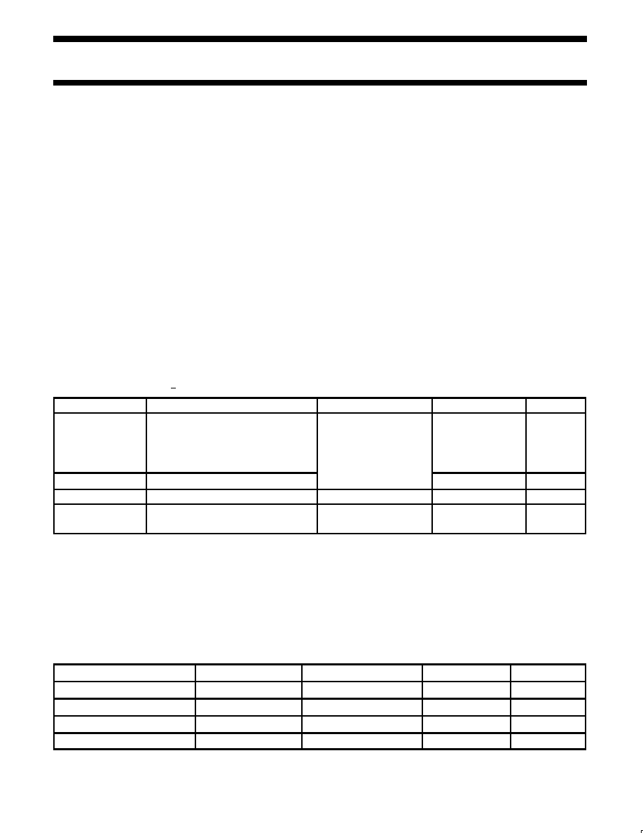
QUICK REFERENCE DATA
GND = 0 V; T
amb
= 25
∞
C; t
r
= t
f
<
2.5 ns
SYMBOL
PARAMETER
CONDITIONS
TYPICAL
UNIT
Propagation delay
C
L
= 15 pF
RS to Q
3
V
CC
=
3.3 V
29
t
PHL
/t
PLH
Q
n
to Q
n+1
6
ns
t
PHL
MR to Q
n
16
f
Maximum clock frequency
99
MHz
f
max
Maximum clock frequency
99
MHz
C
1
Input capacitance
3.5
pF
C
Power dissipation capacitance per package
Notes 1, 2 and 3
40
pF
C
PD
Power dissipation capacitance per package
40
pF
NOTES:
1. C
PD
is used to determine the dynamic power
dissipation (P
D
in
m
W)
P
D
= C
PD
x V
CC
2
x f
i
+
S
(C
L
x V
CC
2
x f
o
) where:
f
i
= input frequency in MHz; C
L
= output load capacity in pF;
f
o
= output frequency in MHz; V
CC
= supply voltage in V;
S
(C
L
x V
CC
2
x f
o
) = sum of the outputs.
2. The condition is V
1
= GND to V
CC
3. For formula on dynamic power dissipation, see the
following pages.
ORDERING INFORMATION
PACKAGES
TEMPERATURE RANGE
OUTSIDE NORTH AMERICA
NORTH AMERICA
PKG. DWG. #
16-Pin Plastic DIL
≠40
∞
C to +125
∞
C
74LV4060 N
74LV4060 N
SOT38-4
16-Pin Plastic SO
≠40
∞
C to +125
∞
C
74LV4060 D
74LV4060 D
SOT109-1
16-Pin Plastic SSOP Type II
≠40
∞
C to +125
∞
C
74LV4060 DB
74LV4060 DB
SOT338-1
16-Pin Plastic TSSOP Type I
≠40
∞
C to +125
∞
C
74LV4060 PW
74LV4060PW DH
SOT403-1
Philips Semiconductors
Product specification
74LV4060
14-stage binary ripple counter with oscillator
1998 Jun 23
3
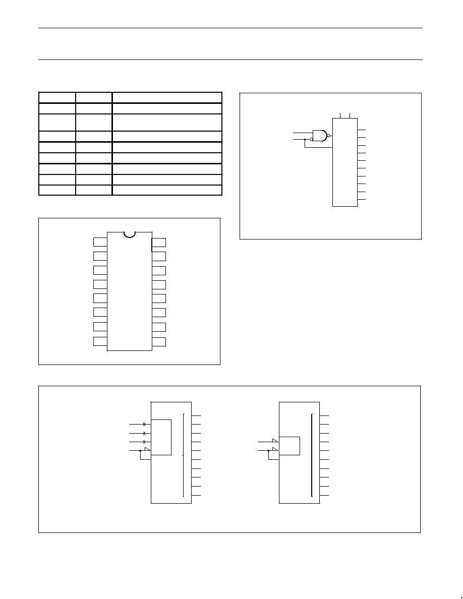
PIN DESCRIPTION
PIN NO.
SYMBOL
FUNCTION
1, 2, 3
Q
11
to Q13
Counter outputs
7, 5, 4, 6,
15, 13, 15
Q
3
to Q
9
Counter outputs
8
GND
Ground (0 V)
9
C
TC
External capacitor connection
10
R
TC
External resistor connection
11
RS
Clock input/oscillator pin
12
MR
Master reset
16
V
CC
Positive supply voltage
PIN CONFIGURATION
SV00308
1
2
3
4
5
6
7
8
9
10
11
12
13
14
15
16
GND
Q
11
Q
12
Q
13
Q
5
Q
4
Q
6
Q
3
C
TC
R
TC
RS
MR
Q
8
Q
7
Q
9
V
CC
LOGIC SYMBOL
1
2
3
4
5
6
7
9
10
12
11
13
14
15
C
TC
R
TC
RS
MR
Q11
Q12
Q13
Q5
Q4
Q6
Q3
Q8
Q7
Q9
SV00307
LOGIC SYMBOL (IEEE/IEC)
9
10
11
12
CX
!G
RX
RCX
CT = 0
+
+
CTR14
(a)
11
13
CT
3
9
1
2
3
4
5
6
7
13
14
15
11
12
&
CT = 0
CTR14
(b)
11
13
CT
3
9
1
2
3
4
5
6
7
13
14
15
SV00311
Philips Semiconductors
Product specification
74LV4060
14-stage binary ripple counter with oscillator
1998 Jun 23
4
DYNAMIC POWER DISSIPATION
GND = 0 V; T
amb
= 25
_
C
PARAMETER
V
CC
(V)
TYPICAL FORMULA FOR P
D
(
m
W)
1
Total dynamic power dissipation when
using the on≠chip oscillator (P
D
)
1.2
2.0
3.0
C
PD
x f
osc
x V
CC
2
+
S
(C
L
x V
CC
2
x f
o
) + 2C
t
x V
CC
2
x f
osc
+ 16 x V
CC
C
PD
x f
osc
x V
CC
2
+
S
(C
L
x V
CC
2
x f
o
) + 2C
t
x V
CC
2
x f
osc
+ 460 x V
CC
C
PD
x f
osc
x V
CC
2
+
S
(C
L
x V
CC
2
x f
o
) + 2C
t
x V
CC
2
x f
osc
+ 1000 x V
CC
NOTE:
1. Where: f
o
= output frequency in MHz; f
osc
= oscillator frequency in MHz;
S
(C
L
x V
CC
2
x f
o
) = sum of the outputs; C
L
= output load capacitance in pF;
C
t
= timing capacitance in pF; V
CC
= supply voltage in V.
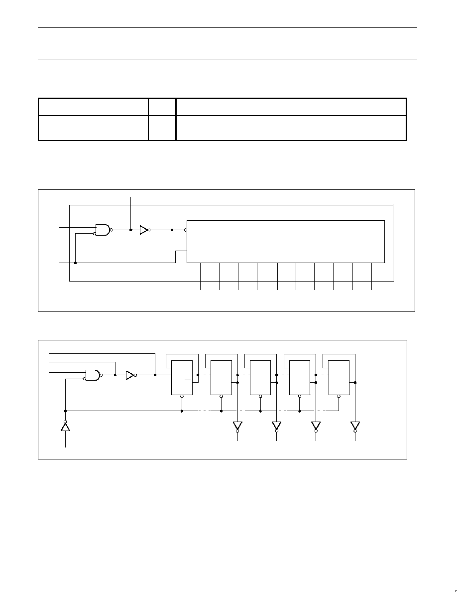
FUNCTIONAL DIAGRAM
9
10
11
12
C
TC
R
TC
RS
MR
C
D
CP
1
Q
11
2
Q
12
3
Q
13
4
Q
5
5
Q
4
6
Q
6
7
Q
3
14-stage binary counter
13
Q
8
14
Q
7
15
Q
9
SV00312
LOGIC DIAGRAM
C
TC
R
TC
RS
MR
Q
11
Q
3
Q
13
Q
9
FF14
FF12
FF10
FF4
CP
FF1
Q
C
D
SV00313
Philips Semiconductors
Product specification
74LV4060
14-stage binary ripple counter with oscillator
1998 Jun 23
5
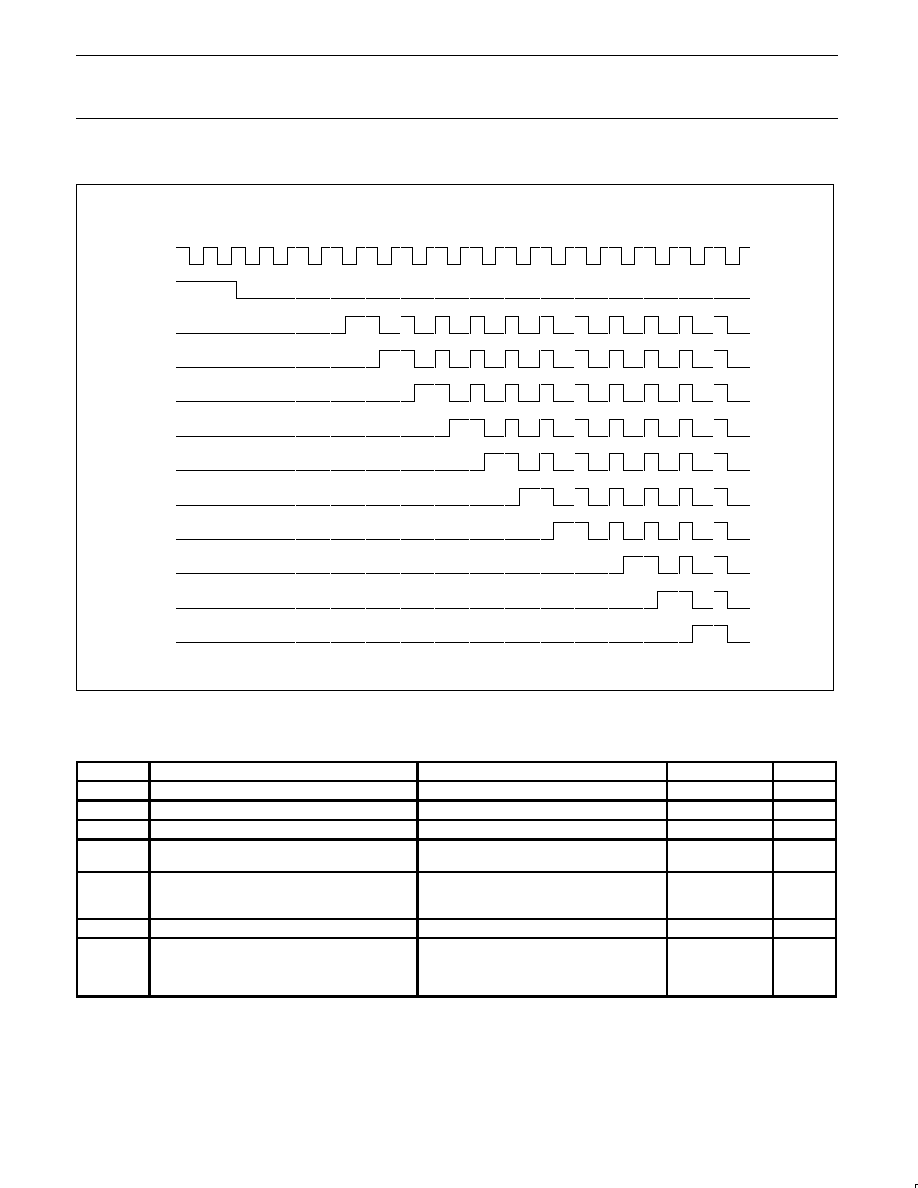
TIMING DIAGRAM
RS
MR
Q3
Q4
Q5
Q6
Q7
Q8
Q9
Q11
Q12
Q13
SV00309
4.096
2.048
1.024
512
256
128
64
32
16
8
4
2
1
8.192
16.384
ABSOLUTE MAXIMUM RATINGS
1, 2
In accordance with the Absolute Maximum Rating System (IEC 134)
Voltages are referenced to GND (ground = 0V)
SYMBOL
PARAMETER
CONDITIONS
RATING
UNIT
V
CC
DC supply voltage
≠0.5 to +7.0
V
±
I
IK
DC input diode current
V
I
< ≠0.5 or V
I
> V
CC
+ 0.5V
20
mA
±
I
OK
DC output diode current
V
O
< ≠0.5 or V
O
> V
CC
+ 0.5V
50
mA
±
I
O
DC output source or sink current
≠ standard outputs
≠0.5V < V
O
< V
CC
+ 0.5V
25
mA
±
I
GND
,
±
I
CC
DC V
CC
or GND current for types with
≠standard outputs
50
mA
T
stg
Storage temperature range
≠65 to +150
∞
C
P
TOT
Power dissipation per package
≠plastic DIL
≠plastic mini-pack (SO)
≠plastic shrink mini-pack (SSOP and TSSOP)
for temperature range: ≠40 to +125
∞
C
above +70
∞
C derate linearly with 12mW/K
above +70
∞
C derate linearly with 8 mW/K
above +60
∞
C derate linearly with 5.5 mW/K
750
500
400
mW
NOTES:
1. Stresses beyond those listed may cause permanent damage to the device. These are stress ratings only and functional operation of the
device at these or any other conditions beyond those indicated under "recommended operating conditions" is not implied. Exposure to
absolute-maximum-rated conditions for extended periods may affect device reliability.
2. The input and output voltage ratings may be exceeded if the input and output current ratings are observed.