Document Outline
- FEATURES
- DESCRIPTION
- QUICK REFERENCE DATA
- ORDERING INFORMATION
- PIN CONFIGURATION
- PIN DESCRIPTION
- IEC LOGIC SYMBOL
- FUNCTIONAL DIAGRAM
- LOGIC SYMBOL
- SCHEMATIC DIAGRAM (ONE SWITCH)
- RECOMMENDED OPERATING CONDITIONS
- ABSOLUTE MAXIMUM RATINGS
- DC ELECTRICAL CHARACTERISTICS
- AC CHARACTERISTICS
- ADDITIONAL AC CHARACTERISTICS
- WAVEFORMS
- TEST CIRCUIT
- PACKAGE OUTLINES
- SOT38-4
- SOT109-1
- SOT338-1
- SOT403-1
- DEFINITIONS
Philips
Semiconductors
74LV4316
Quad bilateral switches
Product specification
Supersedes data of 1994 Dec 01
IC24 Data Handbook
1998 Jun 23
INTEGRATED CIRCUITS

Philips Semiconductors
Product specification
74LV4316
Quad bilateral switches
2
1998 Jun 23
853-2079 19619
FEATURES
∑
Optimized for Low Voltage applications: 1.0V to 6.0V
∑
Accepts TTL input levels between V
CC
= 2.7V and V
CC
= 3.6V
∑
Low typ "ON" resistance:
80
W
at V
CC
≠ VEE = 4.5V
120
W
at V
CC
≠ VEE = 3.0V
295
W
at V
CC
≠ VEE = 2.0V
∑
Logic level translation: to enable 3V logic to communicate
with
"
3V analog signals
∑
Typical "break before make" built in
∑
Output capability: non-standard
∑
I
CC
category: MSI
DESCRIPTION
The 74LV4316 is a low-voltage CMOS device that is pin and
function compatible with 74HC/HCT4316.
The 74LV4316 has four independent analog switches. Each switch
has two input/output terminals (nY, nZ) and an active HIGH select
input (nS). When the enable input (E) is HIGH, all four analog
switches are turned off.
Current through a switch will not cause additional V
CC
current provided
the voltage at the terminals of the switch is maintained within the
supply voltage range; V
CC
>
(V
Y
, V
Z
)
>
V
EE
. Inputs nY and nZ are
electrically equivalent terminals. V
CC
and GND are the supply voltage
pins for the digital control inputs (E and nS). The V
CC
to GND ranges
are 1.0 to 6.0 V.
The analog inputs/outputs (nY and nZ) can swing between V
CC
as a
positive limit and V
EE
as a negative limit.
V
CC
≠ V
EE
may not exceed 6.0 V.
QUICK REFERENCE DATA
GND = 0 V; T
amb
= 25
∞
C; t
r
=t
f
v
2.5 ns
SYMBOL
PARAMETER
CONDITIONS
TYPICAL
UNIT
t
PZH
/t
PZL
Turn "ON" time:
E to V
OS
nS to V
OS
C
L
= 15pF
R
L
= 1K
W
V
CC
= 3.3V
19
ns
t
PHZ
/t
PLZ
Turn "OFF" time:
E to V
OS
nS to V
OS
20
ns
C
I
Input capacitance
3.5
pF
C
PD
Power dissipation capacitance per switch
Notes 1, 2
13
pF
C
S
Maximum switch capacitance
5
pF
NOTES:
1. C
PD
is used to determine the dynamic power dissipation (P
D
in
µ
W)
P
D
= C
PD
◊
V
CC
2
◊
f
i
)
(C
L
◊
V
CC
2
◊
f
o
) where:
f
i
= input frequency in MHz; C
L
= output load capacity in pF;
f
o
= output frequency in MHz; V
CC
= supply voltage in V;
V
CC
= supply voltage in V:
(C
L
◊
V
CC
2
◊
f
o
) = sum of the outputs.
2. The condition is V
I
= GND to V
CC.
ORDERING INFORMATION
PACKAGES
TEMPERATURE RANGE
OUTSIDE NORTH AMERICA
NORTH AMERICA
PKG. DWG. #
16-Pin Plastic DIL
≠40
∞
C to +125
∞
C
74LV4316 N
74LV4316 N
SOT38-4
16-Pin Plastic SO
≠40
∞
C to +125
∞
C
74LV4316 D
74LV4316 D
SOT109-1
16-Pin Plastic SSOP Type II
≠40
∞
C to +125
∞
C
74LV4316 DB
74LV4316 DB
SOT338-1
16-Pin Plastic TSSOP Type I
≠40
∞
C to +125
∞
C
74LV4316 PW
74LV4316PW DH
SOT403-1
PIN CONFIGURATION
SV01650
14
13
12
11
10
9
8
7
6
5
4
3
2
1
15
16
GND
V
CC
1Z
1Y
2Y
2Z
2S
3S
E
1S
4S
4Z
4Y
3Y
3Z
V
EE
PIN DESCRIPTION
PIN
NUMBER
SYMBOL
FUNCTION
1, 4, 10, 13
1Z ≠ 4Z
Independent inputs/outputs
2, 3, 11, 12
1Y ≠ 4Y
Independent inputs/outputs
7
E
Enable input (active LOW)
8
GND
Ground (0V)
9
V
EE
Negative supply voltage
15, 5, 6, 14
1S ≠ 4S
Select inputs (active HIGH)
16
V
CC
Positive supply voltage

Philips Semiconductors
Product specification
74LV4316
Quad bilateral switches
1998 Jun 23
3
IEC LOGIC SYMBOL
SV01658
#
#
#
#
4
10
1
13
3
5
11
6
2
G1
7
(a)
(b)
15
12
14
#
#
#
#
4
10
1
13
3
5
11
6
2
2
1X2
2
G1
7
15
12
14
FUNCTIONAL DIAGRAM
SV01653
1
15
5
6
14
4
10
13
2
3
11
12
1Z
1S
2S
3S
4S
2Z
3Z
4Z
1Y
2Y
3Y
4Y
8
7
9
16
VEE
V CC
GND
E
LOGIC LEVEL
CONVERSION
AND CONTROL
LOGIC SYMBOL
SV01651
15
5
6
14
7
1S
2S
3S
4S
E
13
3
1
4
2
10
11
12
4Z
2Y
1Z
2Z
1Y
3Z
3Y
4Y
SCHEMATIC DIAGRAM (ONE SWITCH)
SV01654
V
CC
nY
V
EE
V
EE
nZ
V
CC
to other switches
E
nS
LOGIC LEVEL
CONVERSION
LOGIC LEVEL
CONVERSION
Philips Semiconductors
Product specification
74LV4316
Quad bilateral switches
1998 Jun 23
4
RECOMMENDED OPERATING CONDITIONS
SYMBOL
PARAMETER
CONDITIONS
MIN
TYP
MAX
UNIT
V
CC
DC supply voltage
See Note 1
1.0
3.3
6.0
V
V
I
Input voltage
0
≠
V
CC
V
V
O
Output voltage
0
≠
V
CC
V
T
amb
Operating ambient temperature range in free air
See DC and AC
characteristics
≠40
≠40
+85
+125
∞
C
t
r
, t
f
Input rise and fall times
V
CC
= 1.0V to 2.0V
V
CC
= 2.0V to 2.7V
V
CC
= 2.7V to 3.6V
V
CC
= 3.6V to 5.5V
≠
≠
≠
≠
≠
≠
≠
≠
500
200
100
50
ns/V
NOTE:
1. The LV is guaranteed to function down to V
CC
= 1.0V (input levels GND or V
CC
); DC characteristics are guaranteed from V
CC
= 1.2V to V
CC
= 5.5V.
ABSOLUTE MAXIMUM RATINGS
1, 2
In accordance with the Absolute Maximum Rating System (IEC 134).
Voltages are referenced to GND (ground = 0 V).
SYMBOL
PARAMETER
CONDITIONS
RATING
UNIT
V
CC
DC supply voltage
≠0.5 to +7.0
V
"
I
IK
DC input diode current
V
I
< ≠0.5 or V
I
> V
CC
+ 0.5V
20
mA
"
I
OK
DC output diode current
V
O
< ≠0.5 or V
O
> V
CC
+ 0.5V
20
mA
"
I
O
DC switch current
≠0.5V < V
O
< V
CC
+ 0.5V
25
mA
T
stg
Storage temperature range
≠65 to +150
∞
C
P
TOT
Power dissipation per package
≠ plastic DIL
≠ plastic mini-pack (SO)
≠ plastic shrink mini-pack (SSOP and TSSOP)
for temperature range: ≠40 to +125
∞
C
above +70
∞
C derate linearly with 12 mW/K
above +70
∞
C derate linearly with 8 mW/K
above +60
∞
C derate linearly with 5.5 mW/K
750
500
400
mW
NOTES:
1. Stresses beyond those listed may cause permanent damage to the device. These are stress ratings only and functional operation of the
device at these or any other conditions beyond those indicated under "recommended operating conditions" is not implied. Exposure to
absolute-maximum-rated conditions for extended periods may affect device reliability.
2. The input and output voltage ratings may be exceeded if the input and output current ratings are observed.

Philips Semiconductors
Product specification
74LV4316
Quad bilateral switches
1998 Jun 23
5
DC ELECTRICAL CHARACTERISTICS
Over recommended operating conditions. Voltages are referenced to GND (ground = 0 V).
LIMITS
SYMBOL
PARAMETER
TEST CONDITIONS
-40
∞
C to +85
∞
C
-40
∞
C to +125
∞
C
UNIT
MIN
TYP
1
MAX
MIN
MAX
V
CC
= 1.2 V
0.90
0.90
HIGH level Input
V
CC
= 2.0 V
1.40
1.4
V
IH
HIGH level Input
voltage
V
CC
= 2.7 to 3.6 V
2.00
2.0
V
voltage
V
CC
= 4.5 V
3.15
3.15
V
CC
= 6.0 V
4.20
4.20
V
CC
= 1.2 V
0.30
0.30
LOW level Input
V
CC
= 2.0 V
0.60
0.60
V
IL
LOW level Input
voltage
V
CC
= 2.7 to 3.6 V
0.80
0.80
V
voltage
V
CC
= 4.5 V
1.35
1.35
V
CC
= 6.0 V
1.80
1.80
±
I
I
Input leakage
current
V
CC
= 3.6 V; V
I
= V
CC
or GND
V
CC
= 6.0 V; V
I
= V
CC
or GND
1.0
2.0
1.0
2.0
µ
A
±
I
S
Analog switch
OFF-state current
per channel
V
CC
= 3.6 V; V
I
= V
IH
or V
IL
V
CC
= 6.0 V; V
I
= V
IH
or V
IL
1.0
2.0
1.0
2.0
µ
A
±
I
S
Analog switch
ON-state current
per channel
V
CC
= 3.6 V; V
I
= V
IH
or V
IL
V
CC
= 6.0 V; V
I
= V
IH
or V
IL
1.0
2.0
1.0
2.0
µ
A
I
CC
Quiescent supply
current
V
CC
= 3.6V; V
I
= V
CC
or GND; I
O
= 0
V
CC
= 6.0V; V
I
= V
CC
or GND; I
O
= 0
20
40
40
80
µ
A
I
CC
Additional
quiescent supply
current per input
V
CC
= 2.7 V to 3.6 V; V
I
= V
CC
≠ 0.6 V
500
850
µ
A
R
ON
ON-resistance
(peak)
V
CC
= 1.2 V; V
I
= V
IH
or V
IL
V
CC
= 2.0 V; V
I
= V
IH
or V
IL
V
CC
= 2.7 V; V
I
= V
IH
or V
IL
V
CC
= 3.0 to 3.6 V; V
I
= V
IH
or V
IL
V
CC
= 4.5 V; V
I
= V
IH
or V
IL
V
CC
= 6.0 V; V
I
= V
IH
or V
IL
295
120
110
80
70
≠
860
300
270
200
180
≠
990
360
325
240
215
R
ON
ON-resistance
(rail)
V
CC
= 1.2 V; V
I
= V
IH
or V
IL
V
CC
= 2.0 V; V
I
= V
IH
or V
IL
V
CC
= 2.7 V; V
I
= V
IH
or V
IL
V
CC
= 3.0 to 3.6 V; V
I
= V
IH
or V
IL
V
CC
= 4.5 V; V
I
= V
IH
or V
IL
V
CC
= 6.0 V; V
I
= V
IH
or V
IL
225
110
85
55
40
35
≠
240
150
135
100
90
≠
290
180
180
120
110
R
ON
ON-resistance
(rail)
V
CC
= 1.2 V; V
I
= V
IH
or V
IL
V
CC
= 2.0 V; V
I
= V
IH
or V
IL
V
CC
= 2.7 V; V
I
= V
IH
or V
IL
V
CC
= 3.0 to 3.6 V; V
I
= V
IH
or V
IL
V
CC
= 4.5 V; V
I
= V
IH
or V
IL
V
CC
= 6.0 V; V
I
= V
IH
or V
IL
250
120
75
60
45
40
≠
270
170
155
115
105
≠
325
205
180
135
120
R
ON
Maximum variation
of ON-resistance
between any two
channels
V
CC
= 1.2 V; V
I
= V
IH
or V
IL
V
CC
= 2.0 V; V
I
= V
IH
or V
IL
V
CC
= 2.7 V; V
I
= V
IH
or V
IL
V
CC
= 3.0 to 3.6 V; V
I
= V
IH
or V
IL
V
CC
= 4.5 V; V
I
= V
IH
or V
IL
V
CC
= 6.0 V; V
I
= V
IH
or V
IL
≠
5
4
4
3
2
NOTE:
1. All typical values are measured at T
amb
= 25
∞
C.
2. At supply voltage approaching 1.2V, the analog switch ON-resistance becomes extremely non-linear. Therefore it is recommended that
these devices be used to transmit digital signals only, when using these supply voltages.
Philips Semiconductors
Product specification
74LV4316
Quad bilateral switches
1998 Jun 23
6
SV01655
V
HIGH
(from select inputs)
I
is
nZ
V
EE
nY
Vis = 0 to V
CC
≠ V
EE
Figure 1.
Test circuit for measuring ON-resistance (R
on).
SV01656
A
LOW
(from select inputs)
nZ
V
EE
nY
V
I
= V
CC
or V
EE
VO= VEE or V
CC
A
Figure 2.
Test circuit for measuring OFF-state current.
SV01657
HIGH
(from select inputs)
nZ
V
EE
nY
V
I
= V
CC
or V
EE
V
O
(open circuit)
A
Figure 3.
Test circuit for measuring ON-state current.
SV01658
0
V
CC
= 2.0 V
V
CC
= 3.0 V
V
CC
= 4.5 V
0
1.2
2.4
3.6
V
is
(V)
4.8
100
50
200
150
250
300
R
ON
(W)
Figure 4.
Typical ON-resistance (R
ON
) as a function of input
voltage (V
is
) for V
is
= 0 to V
CC
≠ V
EE
.

Philips Semiconductors
Product specification
74LV4316
Quad bilateral switches
1998 Jun 23
7
AC CHARACTERISTICS
GND = 0 V; t
r
= t
f
2.5ns; C
L
= 50pF
LIMITS
CONDITION
SYMBOL
PARAMETER
≠40 to +85
∞
C
≠40 to +125
∞
C
UNIT
CONDITION
MIN
TYP
1
MAX
MIN
MAX
V
CC
(V)
OTHER
30
1.2
10
19
24
2.0
R
t
PHL
/t
PLH
Propagation delay
8
14
18
ns
2.7
R
L
=
;
C
L
= 50 pF
t
PHL
/t
PLH
g
y
V
is
to V
os
6
*
11
14
ns
3.0 to 3.6
C
L
= 50 F
Figure 12
5
9
12
4.5
g
4
7
9
6.0
110
1.2
37
70
85
2.0
R
1 k
W
t
PZH
/t
PZL
Turn-on time
28
51
63
ns
2.7
R
L
= 1 k
W
;
C
L
= 50 pF
t
PZH
/t
PZL
E to V
os
21
2
41
50
ns
3.0 to 3.6
C
L
= 50 F
Figures 13 and 14
19
35
43
4.5
gu es 3 a d
15
27
33
6.0
95
1.2
32
61
75
2.0
R
1 k
W
t
PZH
/t
PZL
Turn-on time
24
45
55
ns
2.7
R
L
= 1 k
W
;
C
L
= 50 pF
t
PZH
/t
PZL
nS to V
os
18
2
36
44
ns
3.0 to 3.6
C
L
= 50 F
Figures 13 and 14
16
31
37
4.5
gu es 3 a d
12
23
29
6.0
105
1.2
37
68
80
2.0
R
1 k
W
;
t
PHZ
/t
PLZ
Turn-off time
28
51
59
ns
2.7
R
L
= 1 k
W
;
C
L
= 50 pF
t
PHZ
/t
PLZ
E to V
os
22
2
41
48
ns
3.0 to 3.6
C
L
= 50 F
Figures 13 and 14
20
35
41
4.5
gu es 3 a d
16
28
32
6.0
90
1.2
32
59
70
2.0
R
1 k
W
;
t
PHZ
/t
PLZ
Turn-off time
24
44
52
ns
2.7
R
L
= 1 k
W
;
C
L
= 50 pF
t
PHZ
/t
PLZ
nS to V
os
19
2
36
42
ns
3.0 to 3.6
C
L
= 50 F
Figures 13 and 14
17
31
36
4.5
gu es 3 a d
14
24
28
6.0
NOTES:
1. All typical values are measured at T
amb
= 25
∞
C.
2. All typical values are measured at V
CC
= 3.3V
Philips Semiconductors
Product specification
74LV4316
Quad bilateral switches
1998 Jun 23
8
ADDITIONAL AC CHARACTERISTICS
GND = 0 V; t
r
= t
f
2.5ns; C
L
= 50pF
SYMBOL
PARAMETER
TYP
UNIT
V
CC
(V)
V
IS(P≠P)
(V)
CONDITIONS
Sine-wave distortion f = 1 kHz
0.80
%
3.0
2.75
R
L
= 10 k
W
; C
L
= 50 pF
Sine-wave distortion f = 1 kHz
0.40
%
6.0
5.50
L
L
Figure 10
Sine-wave distortion f = 10 kHz
2.40
%
3.0
2.75
R
L
= 10 k
W
; C
L
= 50 pF
Sine-wave distortion f = 10 kHz
1.20
%
6.0
5.50
L
L
Figure 10
Switch "OFF" signal feed through
≠50
dB
3.0
Note 1
R
L
= 600 k
W
; C
L
= 50 pF; f=1 MHz
Switch OFF signal feed through
≠50
dB
6.0
L
L
Figures 5 and 11
Crosstalk between any two switches
≠60
dB
3.0
Note 1
R
L
= 600 k
W
; C
L
= 50 pF; f=1 MHz
Crosstalk between any two switches
≠60
dB
6.0
L
L
Figure 7
V
(
)
Crosstalk voltage between enable or address
110
mV
3.0
R
L
= 600 k
W
; C
L
= 50 pF; f=1 MHz
(nS or E square wave between V
CC
V
(p≠p)
g
input to any switch (peak-to-peak value)
220
mV
6.0
(nS or E, square wave between V
CC
and GND, T
r
= t
f
= 6 ns) Figure 8
f
Minimum frequency response (≠3 dB)
180
mHz
3.0
Note 2
R
L
= 50 k
W
; C
L
= 50 pF
f
max
Minimum frequency res onse (≠3 dB)
200
mHz
6.0
L
L
Figures 6 and 9
C
S
Maximum switch capacitance
5
pF
GENERAL NOTES:
V
is
is the input voltage at nY or nZ terminal, whichever is assigned as an input.
V
os
is the output voltage at nY or nZ terminal, whichever is assigned as an output.
NOTES:
1. Adjust input voltage V
is
is 0 dBm level (0 dBm = 1 mW into 600
W
).
2. Adjust input voltage V
is
is 0 dBm level at V
os
for 1 MHz (0 dBm = 1 mW into 50
W
).
SV01635
(dB)
f (kHz)
0
10
10
2
10
3
10
4
10
5
10
6
≠50
≠100
Figure 5. Typical switch "OFF" signal feed-through as a
function of frequency.
SV01664
(dB)
f (kHz)
5
10
10 2
10 3
10 4
10 5
10 6
0
≠
5
Figure 6. Typical frequency response.
NOTES TO FIGURES 5 AND 6:
Test conditions: V
CC
= 3.0 V; GND = 0 V; R
L
= 50
W
; R
SOURCE
= 1k
W
.
SV01665
GND
2R
L
V
CC
channel
ON
V
is
0.1
m
F
R
L
nY/nZ
nZ/nY
C
L
GND
channel
OFF
(b)
(a)
V
os
dB
2R
L
nY/nZ
2R
L
2R
L
V
CC
V
CC
nZ/nY
2R
L
C
L
R
L
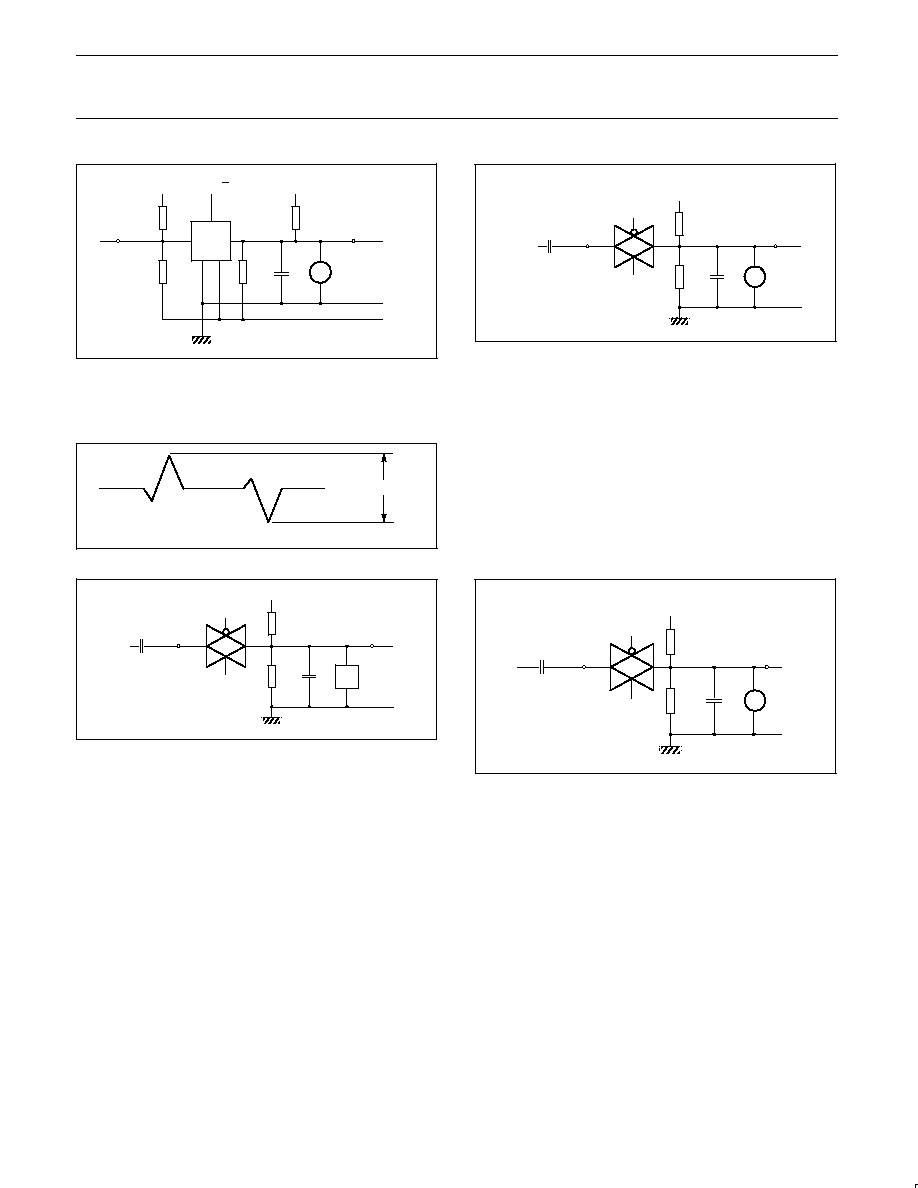
Figure 7. Test circuit for measuring crosstalk between any two switches.
(a) channel ON condition; (b) channel OFF condition.
Philips Semiconductors
Product specification
74LV4316
Quad bilateral switches
1998 Jun 23
9
SV01666
GND
VEE
2R
L
2R
L
V
CC
V
CC
nS or E
nY/nZ
nZ/nY
2R
L
2R
L
C
L
oscilloscope
DUT
Figure 8. Test circuit for measuring
crosstalk between control and any switch.
NOTE TO FIGURE 8:
The crosstalk is defined as follows (oscilloscope output):
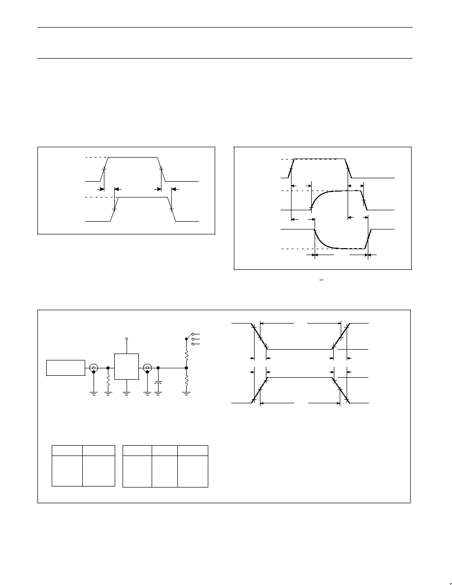
SV01642
V(p ≠ p)
SV01667
GND
channel
ON
V
os
dB
nY/nZ
2R
L
V
CC
nZ/nY
2R
L
C
L
0.1 mF
~
sine-wave
V
is
Figure 9. Test circuit for measuring
minimum frequency response.
NOTE TO FIGURE 9:
Adjust input voltage to obtain 0 dBm at V
OS
when F
in
= 1 MHz. After
set-up frequency of f
in
is increased to obtain a reading of ≠3 dB at V
OS.
f
in
1 kHz
sine-wave
nY/nZ
SV01668
GND
channel
ON
V
os
distortion
meter
2R
L
V
CC
nZ/nY
2R
L
C
L
10
m
F
Figure 10. Test circuit for measuring sine-wave distortion.
SV01639
GND
2R
L
V
CC
channel
OFF
V
is
0.1
m
F
Y
n
/Z
Z/Y
n
dB
C
L
2R
L
V
OS
Figure 11. Test circuit for measuring
switch "OFF" signal feed-through.
Philips Semiconductors
Product specification
74LV4316
Quad bilateral switches
1998 Jun 23
10
WAVEFORMS
V
M
= 1.5 V at 2.7 V
V
CC
3.6 V
V
M
= 0.5
◊
V
CC
at 2.7 V
>
V
CC
>
3.6 V
V
OL
and V
OH
are the typical output voltage drop that occur with the
output load
V
x
= V
OL
+ 0.3 V at 2.7 V
V
CC
3.6 V
V
X
= V
OL
+ 0.1
◊
V
CC
at 2.7 V
>
V
CC
>
3.6 V
V
Y
= V
OH
≠ 0.3 V at 2.7 V
V
CC
3.6 V
V
Y
= V
OH
≠ 0.1
◊
V
CC
at 2.7 V
>
V
CC
>
3.6 V
SV01638
V M
V M
INPUTS
OUTPUTS
GND
V OL
V I
V OH
tPHL
tPLH
Figure 12. Input (V
is
) to output (V
os
) propagation delays.
SV01640
outputs
disabled
outputs
enabled
outputs
enabled
t
PHZ
t
PZH
t
PZL
t
PLZ
V
X
V
Y
V
M
V
M
V
M
INPUTS
OUTPUT
HIGH-to-OFF
OFF-to-HIGH
OUTPUT
LOW-to-OFF
OFF-to-LOW
GND
V
CC
V
I
V
OL
V
OH
GND
Figure 13. Turn-on and turn-off times
for the inputs (nS, E) to the output (V
os
).
TEST CIRCUIT
V
M
V
M
t
W
NEGATIVE
PULSE
10%
10%
90%
90%
0V
V
M
V
M
t
W
V
I
POSITIVE
PULSE
90%
90%
10%
10%
0V
t
THL
(t
f
)
t
TLH
(t
r
)
t
THL
(t
f
)
t
TLH
(t
r
)
V
M
= 1.5V
Input Pulse Definition
SY00044
SWITCH POSITION
PULSE
GENERATOR
R
T
V
l
D.U.T.
V
O
C
L
= 50pF
R
L
= 1k
V
cc
Test Circuit for Outputs
Open
GND
S
1
V
S1
DEFINITIONS
V
CC
V
I
< 2.7V
2.7≠3.6V
V
CC
2.7V
TEST
S
1
t
PLZ/
t
PZL
t
PLH/
t
PHL
t
PHZ
/t
PZH
V
S1
Open
GND
V
S1
4.5 V
2
<
V
CC
V
CC
2
<
V
CC
R
L
= Load resistor
C
L
= Load capacitance includes jig and probe capacitance
R
T
= Termination resistance should be equal to Z
OUT
of
pulse generators.
V
I
2
<
V
CC
R
L
= 1k
Figure 14. Load circuitry for switching times.

Philips Semiconductors
Product specification
74LV4316
Quad bilateral latches
1998 Jun 23
11
DIP16:
plastic dual in-line package; 16 leads (300 mil)
SOT38-4
Philips Semiconductors
Product specification
74LV4316
Quad bilateral latches
1998 Jun 23
12
SO16:
plastic small outline package; 16 leads; body width 3.9 mm
SOT109-1

Philips Semiconductors
Product specification
74LV4316
Quad bilateral latches
1998 Jun 23
13
SSOP16:
plastic shrink small outline package; 16 leads; body width 5.3 mm
SOT338-1
Philips Semiconductors
Product specification
74LV4316
Quad bilateral latches
1998 Jun 23
14
TSSOP16:
plastic thin shrink small outline package; 16 leads; body width 4.4 mm
SOT403-1

Philips Semiconductors
Product specification
74LV4316
Quad bilateral latches
1998 Jun 23
15
NOTES
Philips Semiconductors
Product specification
74LV4316
Quad bilateral switches
yyyy mmm dd
16
Philips Semiconductors and Philips Electronics North America Corporation reserve the right to make changes, without notice, in the products,
including circuits, standard cells, and/or software, described or contained herein in order to improve design and/or performance. Philips
Semiconductors assumes no responsibility or liability for the use of any of these products, conveys no license or title under any patent, copyright,
or mask work right to these products, and makes no representations or warranties that these products are free from patent, copyright, or mask
work right infringement, unless otherwise specified. Applications that are described herein for any of these products are for illustrative purposes
only. Philips Semiconductors makes no representation or warranty that such applications will be suitable for the specified use without further testing
or modification.
LIFE SUPPORT APPLICATIONS
Philips Semiconductors and Philips Electronics North America Corporation Products are not designed for use in life support appliances, devices,
or systems where malfunction of a Philips Semiconductors and Philips Electronics North America Corporation Product can reasonably be expected
to result in a personal injury. Philips Semiconductors and Philips Electronics North America Corporation customers using or selling Philips
Semiconductors and Philips Electronics North America Corporation Products for use in such applications do so at their own risk and agree to fully
indemnify Philips Semiconductors and Philips Electronics North America Corporation for any damages resulting from such improper use or sale.
This data sheet contains preliminary data, and supplementary data will be published at a later date. Philips
Semiconductors reserves the right to make changes at any time without notice in order to improve design
and supply the best possible product.
Philips Semiconductors
811 East Arques Avenue
P.O. Box 3409
Sunnyvale, California 94088≠3409
Telephone 800-234-7381
DEFINITIONS
Data Sheet Identification
Product Status
Definition
Objective Specification
Preliminary Specification
Product Specification
Formative or in Design
Preproduction Product
Full Production
This data sheet contains the design target or goal specifications for product development. Specifications
may change in any manner without notice.
This data sheet contains Final Specifications. Philips Semiconductors reserves the right to make changes
at any time without notice, in order to improve design and supply the best possible product.
Philips Semiconductors and Philips Electronics North America Corporation
register eligible circuits under the Semiconductor Chip Protection Act.
©
Copyright Philips Electronics North America Corporation 1998
All rights reserved. Printed in U.S.A.
print code
Date of release: 05-96
Document order number:
9397-750-04663
Philips
Semiconductors