Philips Semiconductors
Product specification
74LV573
Octal D-type transparent latch (3-State)
2
1998 Jun 10
853-1989 19545
FEATURES
·
Wide operating voltage: 1.0 to 5.5V
·
Optimized for Low Voltage applications: 1.0V to 3.6V
·
Accepts TTL input levels between V
CC
= 2.7V and V
CC
= 3.6V
·
Typical V
OLP
(output ground bounce) < 0.8V at V
CC
= 3.3V,
T
amb
= 25
°
C
·
Typical V
OHV
(output V
OH
undershoot) > 2V at V
CC
= 3.3V,
T
amb
= 25
°
C
·
Inputs and outputs on opposite sides of package allowing easy
interface with microprocessors
·
Useful as input or output port for microprocessors/microcomputer
·
Common 3-State output enable input
·
Output capability: bus driver
·
I
CC
category: MSI
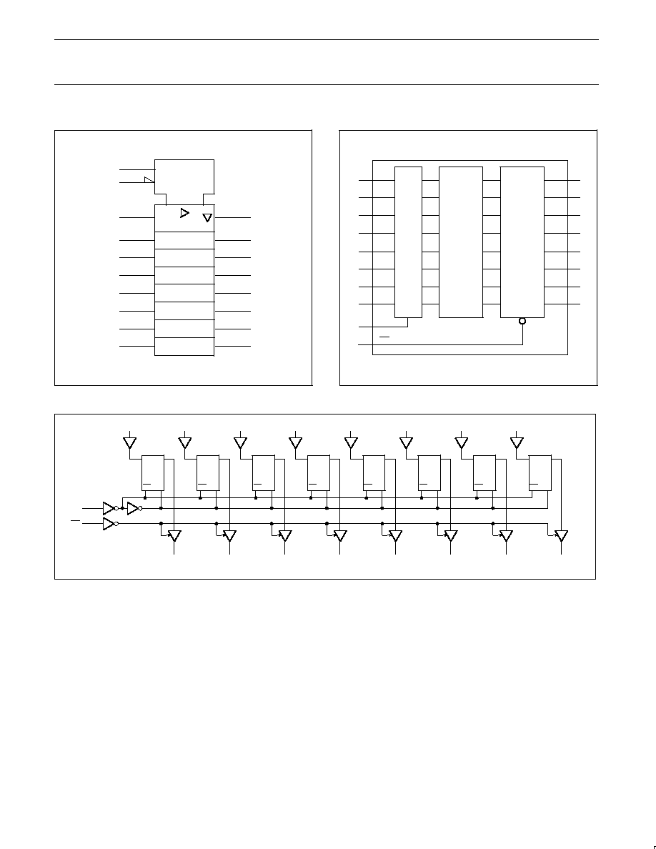
DESCRIPTION
The 74LV573 is a low-voltage Si-gate CMOS device that is pin and
function compatible with 74HC/HCT573.
The 74LV573 is an octal D-type transparent latch featuring separate
D-type inputs for each latch and 3-State outputs for bus oriented
applications. A latch enable (LE) input and an output enable (OE)
input are common to all internal latches.
The `573' consists of eight D-type transparent latches with 3-State
true outputs. When LE is HIGH, data at the D
n
inputs enters the
latches. In this condition the latches are transparent, i.e., a latch
output will change each time its corresponding D-input changes.
When LE is LOW the latches store the information that was present
at the D-inputs a set-up time preceding the HIGH-to-LOW transition
of LE. When OE is LOW, the contents of the eight latches are
available at the outputs. When OE is HIGH, the outputs go to the
high impedance OFF-state. Operation of the OE input does not
affect the state of the latches.
The `573' is functionally identical to the `563' and the `373', but the
`563' has inverted outputs and the `373' has a different pin
arrangement.
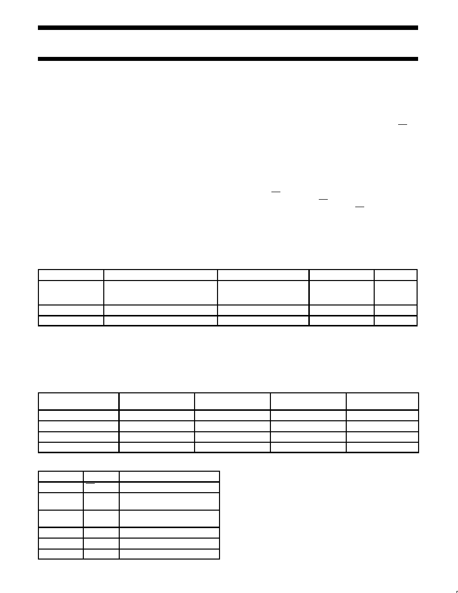
QUICK REFERENCE DATA
GND = 0V; T
amb
= 25
°
C; t
r
= t
f
v
2.5 ns
SYMBOL
PARAMETER
CONDITIONS
TYPICAL
UNIT
t
PHL
/t
PLH
Propagation delay
Dn to Qn
LE to Qn
C
L
= 15pF
V
CC
= 3.3V
12
13
ns
C
I
Input capacitance
3.5
pF
C
PD
Power dissipation capacitance per latch
Notes 1, 2
26
pF
NOTES:
1. C
PD
is used to determine the dynamic power dissipation (P
D
in
µ
W)
P
D
= C
PD
V
CC
2
x f
i
)
(C
L
V
CC
2
f
o
) where:
f
i
= input frequency in MHz; C
L
= output load capacity in pF;
f
o
= output frequency in MHz; V
CC
= supply voltage in V;
(C
L
V
CC
2
f
o
) = sum of the outputs.
2. The condition is V
I
= GND to V
CC.
ORDERING AND PACKAGE INFORMATION
PACKAGES
TEMPERATURE RANGE
OUTSIDE NORTH
AMERICA
NORTH AMERICA
PKG. DWG. #
20-Pin Plastic DIL
40
°
C to +125
°
C
74LV573 N
74LV573 N
SOT146-1
20-Pin Plastic SO
40
°
C to +125
°
C
74LV573 D
74LV573 D
SOT163-1
20-Pin Plastic SSOP Type II
40
°
C to +125
°
C
74LV573 DB
74LV573 DB
SOT339-1
20-Pin Plastic TSSOP Type I
40
°
C to +125
°
C
74LV573 PW
74LV573PW DH
SOT360-1
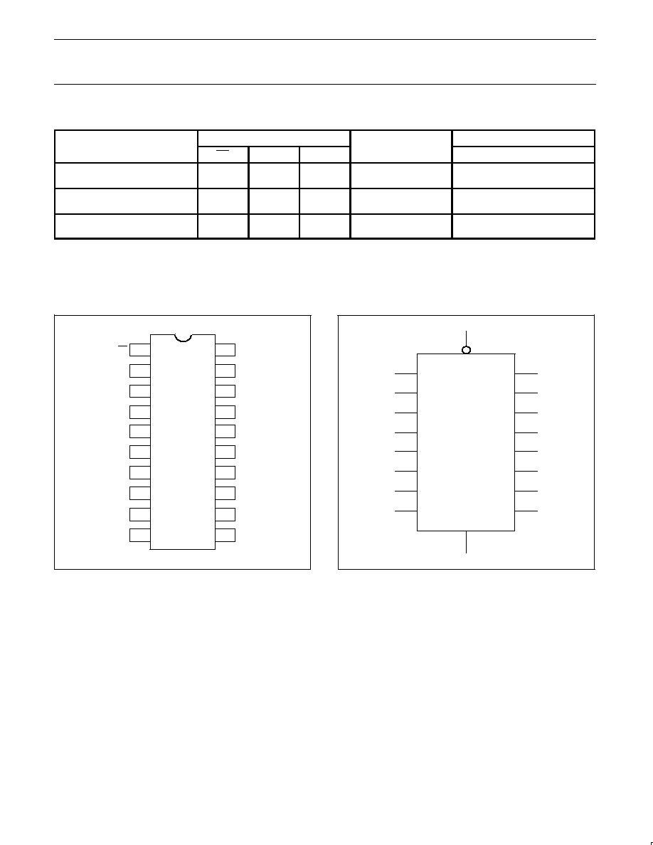
PIN DESCRIPTION
PIN NUMBER
SYMBOL
FUNCTION
1
OE
Output enabled input (active LOW)
2, 3, 4, 5,
6, 7, 8, 9
D0D7
Data inputs
19, 18, 17, 16,
15, 14, 13, 12
Q0Q7
Data outputs
10
GND
Ground (0V)
11
LE
Latch enable input (active HIGH)
20
VCC
Positive supply voltage
Philips Semiconductors
Product specification
74LV573
Octal D-type transparent latch (3-State)
1998 Jun 10
3
FUNCTION TABLE
OPERATING MODES
INPUTS
INTERNAL
OUTPUTS
OPERATING MODES
OE
LE
Dn
LATCHES
Q0 to Q7
Enable and read register
(transparent mode)
L
L
H
H
L
H
L
H
L
H
Latch and read register
L
L
L
L
I
h
L
H
L
H
Latch register and disable outputs
H
H
L
L
I
h
L
H
Z
Z
H = HIGH voltage level
h
= HIGH voltage level one set-up time prior to the HIGH-to-LOW LE transition
L
= LOW voltage level
I
= LOW voltage level one set-up time prior to the HIGH-to-LOW LE transition
Z = High impedance OFF-state
PIN CONFIGURATION
SV00701
1
2
3
4
5
6
7
8
9
11
12
13
14
15
16
17
18
19
20
10
OE
D0
D1
D2
D3
D4
D5
D6
D7
GND
VCC
Q0
Q1
Q2
Q3
Q4
Q5
Q6
Q7
LE
LOGIC SYMBOL
SV00702
OE
LE
Q0
Q1
Q2
Q3
Q4
Q5
Q6
Q7
D0
D1
D2
D3
D4
D5
D6
D7
11
1
2
3
4
5
6
7
8
9
19
18
17
16
15
14
13
12
Philips Semiconductors
Product specification
74LV573
Octal D-type transparent latch (3-State)
1998 Jun 10
5
ABSOLUTE MAXIMUM RATINGS
1, 2
In accordance with the Absolute Maximum Rating System (IEC 134)
Voltages are referenced to GND (ground = 0V)
SYMBOL
PARAMETER
CONDITIONS
RATING
UNIT
V
CC
DC supply voltage
0.5 to +7.0
V
±
I
IK
DC input diode current
V
I
< 0.5 or V
I
> V
CC
+ 0.5V
20
mA
±
I
OK
DC output diode current
V
O
< 0.5 or V
O
> V
CC
+ 0.5V
50
mA
±
I
O
DC output source or sink current
bus driver outputs
0.5V < V
O
< V
CC
+ 0.5V
35
mA
±
I
GND
,
±
I
CC
DC V
CC
or GND current for types with
bus driver outputs
70
mA
T
stg
Storage temperature range
65 to +150
°
C
Power dissipation per package
for temperature range: 40 to +125
°
C
P
t t
plastic DIL
above +70
°
C derate linearly with 12mW/K
750
mW
P
tot
plastic mini-pack (SO)
above +70
°
C derate linearly with 8 mW/K
500
mW
plastic shrink mini-pack (SSOP and TSSOP)
above +60
°
C derate linearly with 5.5 mW/K
400
NOTES:
1. Stresses beyond those listed may cause permanent damage to the device. These are stress ratings only and functional operation of the
device at these or any other conditions beyond those indicated under "recommended operating conditions" is not implied. Exposure to
absolute-maximum-rated conditions for extended periods may affect device reliability.
2. The input and output voltage ratings may be exceeded if the input and output current ratings are observed.
RECOMMENDED OPERATING CONDITIONS
SYMBOL
PARAMETER
CONDITIONS
MIN
TYP.
MAX
UNIT
V
CC
DC supply voltage
See Note 1
1.0
3.3
5.5
V
V
I
Input voltage
0
V
CC
V
V
O
Output voltage
0
V
CC
V
T
amb
Operating ambient temperature range in free
air
See DC and AC
characteristics
40
40
+85
+125
°
C
t
r
, t
f
Input rise and fall times
V
CC
= 1.0V to 2.0V
V
CC
= 2.0V to 2.7V
V
CC
= 2.7V to 3.6V
V
CC
= 3.6V to 5.5V
500
200
100
50
ns/V
NOTE:
1. The LV is guaranteed to function down to V
CC
= 1.0V (input levels GND or V
CC
); DC characteristics are guaranteed from V
CC
= 1.2V to V
CC
= 5.5V.