 | ÐлекÑÑоннÑй компоненÑ: 74LVC109A | СкаÑаÑÑ:  PDF PDF  ZIP ZIP |
Dual JK(not) flip-flop with set and reset; positive-edge trigger
Philips
Semiconductors
74LVC109
Dual JK flip-flop with set and reset;
positive-edge trigger
Product specification
Supersedes data of 1997 Mar 18
IC24 Data Handbook
1998 Apr 28
INTEGRATED CIRCUITS
Philips Semiconductors
Product specification
74LVC109
Dual JK flip-flop with set and reset; positive-edge trigger
2
1998 Apr 28
8531947 19308
FEATURES
·
Wide supply voltage range of 1.2 to 3.6 V
·
In accordance with JEDEC standard no. 8-1A.
·
Inputs accept voltages up to 5.5 V
·
CMOS low power consumption
·
Direct interface with TTL levels
·
Output capability: standard
·
I
CC
category: flip-flops
DESCRIPTION
The 74LVC109 is a low-voltage Si-gate CMOS device that is pin and
function compatible with 74HC/HCT109.
The 74LVC109 is a dual positive-edge triggered JK-type flip-flop
featuring individual J, K inputs, clock (CP) inputs, set (S
D
) and reset
(R
D
) inputs; also complementary Q and Q outputs.
The set and reset are asynchronous active LOW inputs and operate
independently of the clock input.
The J and K inputs control the state changes of the flip-flops as
described in the mode select function table. The J and K inputs must
be stable one set-up time prior to the LOW-to-HIGH clock transition
for predictable operation. The JK design allows operation as a
D-type flip-flop by tying the J and K inputs together.
Schmitt-trigger action in the clock input makes the circuit highly
tolerant to slower clock rise and fall times.
QUICK REFERENCE DATA
GND = 0 V; T
amb
= 25
°
C; t
r
= t
f
2.5 ns
SYMBOL
PARAMETER
CONDITIONS
TYPICAL
UNIT
t
PHL
/t
PLH
Propagation delay
nCP to nQ, nQ
nS
D
to nQ, nQ
nR
D
to nQ, nQ
C
L
= 50 pF;
V
CC
= 3.3 V
4.0
4.5
4.5
ns
f
max
Maximum clock frequency
250
MHz
C
I
Input capacitance
5.0
pF
C
PD
Power dissipation capacitance per flip-flop
V
I
= GND to V
CC
1
27
pF
NOTE:
1. C
PD
is used to determine the dynamic power dissipation (P
D
in
µ
W)
P
D
= C
PD
×
V
CC
2
×
f
i
)
(C
L
×
V
CC
2
×
f
o
) where:
f
i
= input frequency in MHz; C
L
= output load capacity in pF;
f
o
= output frequency in MHz; V
CC
= supply voltage in V;
(C
L
×
V
CC
2
×
f
o
) = sum of the outputs.
ORDERING INFORMATION
PACKAGES
TEMPERATURE RANGE
OUTSIDE NORTH AMERICA
NORTH AMERICA
PKG. DWG. #
16-Pin Plastic SO
40
°
C to +85
°
C
74LVC109 D
74LVC109 D
SOT109-1
16-Pin Plastic SSOP Type II
40
°
C to +85
°
C
74LVC109 DB
74LVC109 DB
SOT338-1
16-Pin Plastic TSSOP Type I
40
°
C to +85
°
C
74LVC109 PW
74LVC109PW DH
SOT403-1
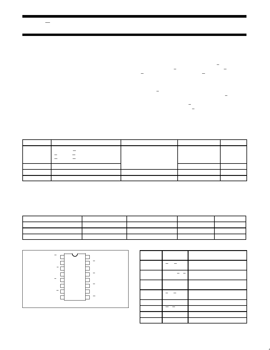
PIN CONFIGURATION
SV00517
1R
D
1K
1CP
1S D
V
CC
2R
D
2J
2K
2CP
2S
D
2Q
2Q
1J
1Q
1Q
GND
14
13
12
11
10
9
8
1
2
3
4
5
6
7
16
15
PIN DESCRIPTION
PIN
NUMBER
SYMBOL
FUNCTION
1, 15
1R
D
, 2R
D
Asynchronous reset input
(active LOW)
2, 14, 3, 13
1J, 2J, 1K, 2K
Synchronous inputs;
flip-flops 1 and 2
4, 12
1CP, 2CP
Clock input
(LOW-to-HIGH, edge-triggered)
5, 11
1S
D,
2S
D
Asynchronous set inputs
(active LOW)
6, 10
1Q, 2Q
True flip-flop outputs
7, 9
1Q, 2Q
Complement flip-flop outputs
8
GND
Ground (O V)
16
V
CC
Positive supply voltage
Philips Semiconductors
Product specification
74LVC109
Dual JK flip-flop with set and reset; positive-edge trigger
1998 Apr 28
3
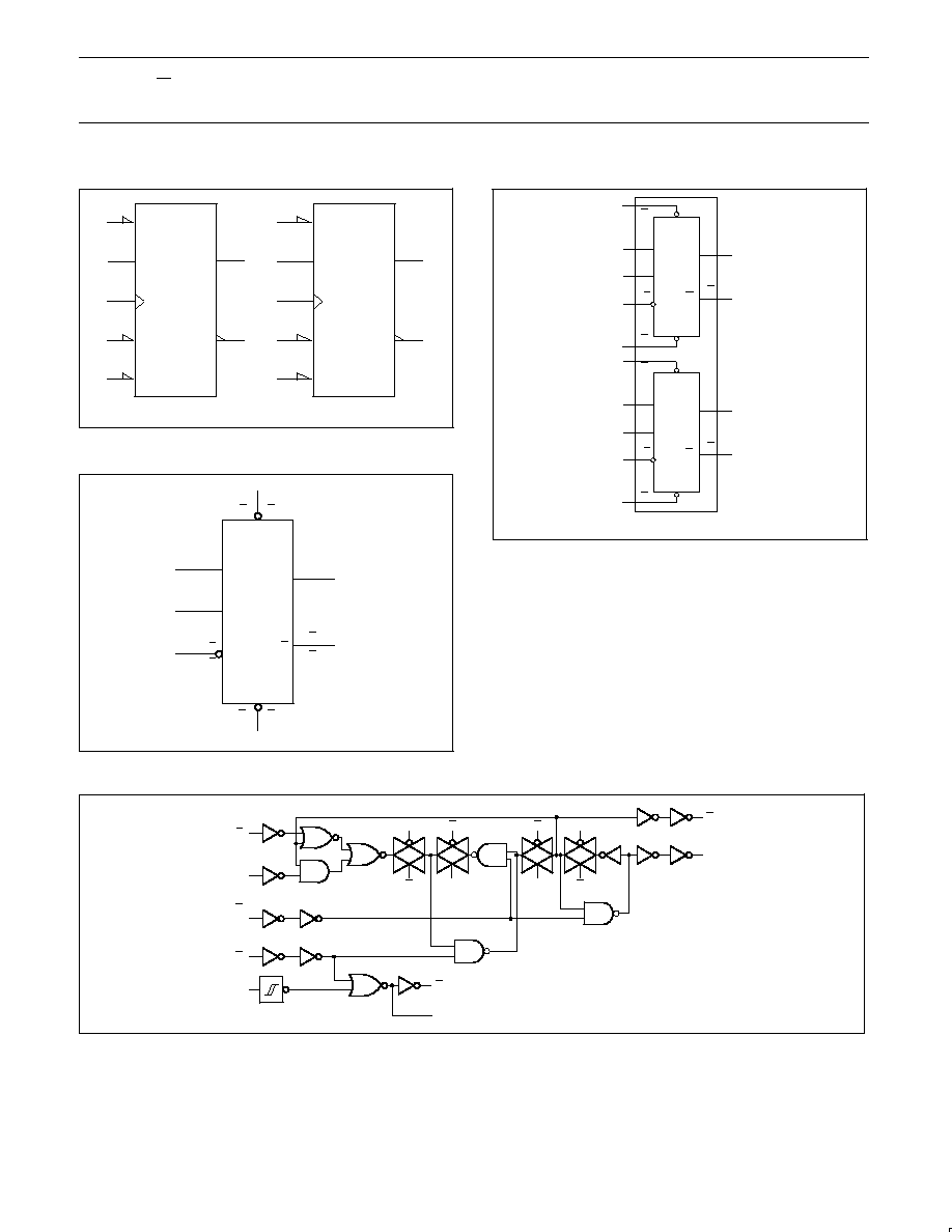
LOGIC SYMBOL (IEEE/IEC)
SV00519
(a)
(b)
6
10
7
9
S
1J
C1
1K
R
2
5
4
3
1
S
1J
C1
1K
R
14
11
12
13
15
LOGIC SYMBOL
SV00518
Q
11
15
2SD
2RD
1SD
1R D
5
1
Q
J
CP
K
1Q 6
2Q 10
1Q 7
2Q 9
14 2J
2 1J
4 1CP
12 2CP
3 1K
13 2K
FUNCTIONAL DIAGRAM
1S
D
SV00520
Q
Q
2S
D
5
11
1R
D
2R
D
R
D
1
15
Q
Q
J
J
CP
FF1
FF2
CP
K
K
1Q
6
10
2Q
1Q
2Q
7
9
2
14
1J
2J
1CP
2CP
4
12
3
13 2K
1K
S
D
S
D
R
D
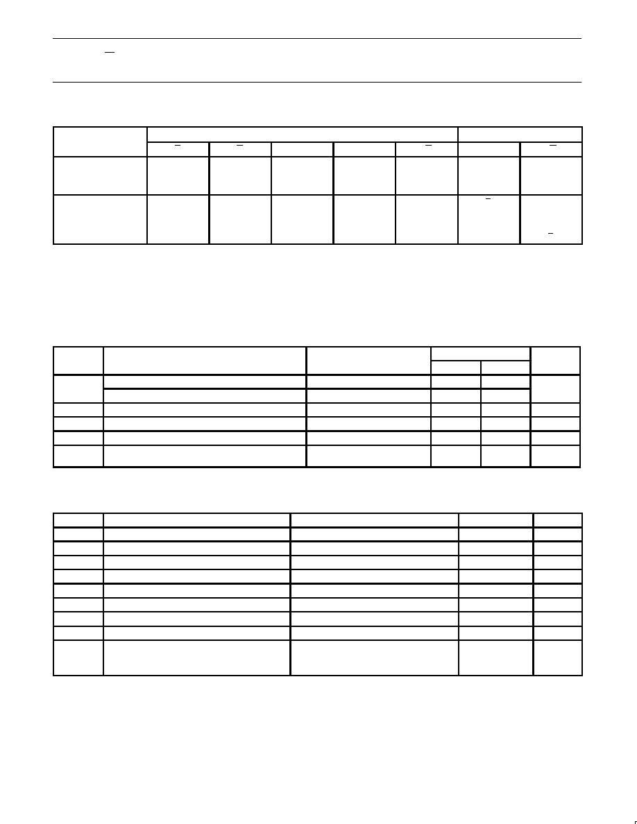
LOGIC DIAGRAM
SV00521
C
C
C
C
C
C
C
C
C
CP
R
J
K
Q
Q
C
S
Philips Semiconductors
Product specification
74LVC109
Dual JK flip-flop with set and reset; positive-edge trigger
1998 Apr 28
4
FUNCTION TABLE
OPERATING MODES
INPUTS
OUTPUTS
OPERATING MODES
nS
D
nR
D
nCP
nJ
nK
nQ
nQ
Asynchronous set
L
H
X
X
X
H
L
Asynchronous reset
H
L
X
X
X
L
H
Undetermined
L
L
X
X
X
H
H
Toggle
H
H
h
l
q
q
Load "0" (reset)
H
H
l
l
L
H
Load "1" (set)
H
H
h
h
H
L
Hold "no change"
H
H
l
h
q
q
NOTES:
H = HIGH voltage level
h = HIGH voltage level one set-up time prior to the LOW-to-HIGH CP transition
L = LOW voltage level
I = LOW voltage level one set-up time prior to the LOW-to-HIGH CP transition
q = lower case letters indicate the state of the referenced output one set-up time prior to the LOW-to-HIGH CP transition.
X = don't care
= LOW-to-HIGH CP transition
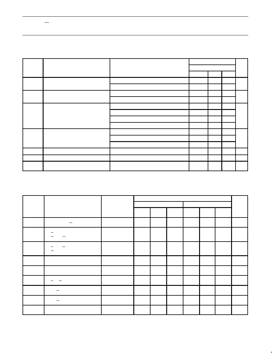
RECOMMENDED OPERATING CONDITIONS
SYMBOL
PARAMETER
CONDITIONS
LIMITS
UNIT
SYMBOL
PARAMETER
CONDITIONS
MIN
MAX
UNIT
V
CC
DC supply voltage (for max. speed performance)
2.7
3.6
V
V
CC
DC supply voltage (for low-voltage applications)
1.2
3.6
V
V
I
DC input voltage range
0
5.5
V
V
O
DC output voltage range
0
V
CC
V
T
amb
Operating free-air temperature range
40
+85
°
C
t
r
, t
f
Input rise and fall times
V
CC
= 1.2 to 2.7V
V
CC
= 2.7 to 3.6V
0
0
20
10
ns/V
ABSOLUTE MAXIMUM RATINGS
1
In accordance with the Absolute Maximum Rating System (IEC 134).
Voltages are referenced to GND (ground = 0V).
SYMBOL
PARAMETER
CONDITIONS
RATING
UNIT
V
CC
DC supply voltage
0.5 to +6.5
V
I
IK
DC input diode current
V
I
t
0
50
mA
V
I
DC input voltage
Note 2
0.5 to +5.5
V
I
OK
DC output diode current
V
O
u
V
CC
or V
O
t
0
"
50
mA
V
O
DC output voltage
Note 2
0.5 to V
CC
+0.5
V
I
O
DC output source or sink current
V
O
= 0 to V
CC
"
50
mA
I
GND
, I
CC
DC V
CC
or GND current
"
100
mA
T
stg
Storage temperature range
65 to +150
°
C
Power dissipation per package
P
TOT
plastic mini-pack (SO)
above +70
°
C derate linearly with 8 mW/K
500
mW
plastic shrink mini-pack (SSOP and TSSOP)
above +60
°
C derate linearly with 5.5 mW/K
500
mW
NOTES:
1. Stresses beyond those listed may cause permanent damage to the device. These are stress ratings only and functional operation of the
device at these or any other conditions beyond those indicated under "recommended operating conditions" is not implied. Exposure to
absolute-maximum-rated conditions for extended periods may affect device reliability.
2. The input and output voltage ratings may be exceeded if the input and output current ratings are observed.
Philips Semiconductors
Product specification
74LVC109
Dual JK flip-flop with set and reset; positive-edge trigger
1998 Apr 28
5
DC ELECTRICAL CHARACTERISTICS
Over recommended operating conditions. Voltages are referenced to GND (ground = 0V).
LIMITS
SYMBOL
PARAMETER
TEST CONDITIONS
Temp = -40
°
C to +85
°
C
UNIT
MIN
TYP
1
MAX
V
HIGH level Input voltage
V
CC
= 1.2V
V
CC
V
V
IH
HIGH level Input voltage
V
CC
= 2.7 to 3.6V
2.0
V
V
LOW level Input voltage
V
CC
= 1.2V
GND
V
V
IL
LOW level Input voltage
V
CC
= 2.7 to 3.6V
0.8
V
V
CC
= 2.7V; V
I
= V
IH
or V
IL
; I
O
= 12mA
V
CC
*
0.5
V
O
HIGH level output voltage
V
CC
= 3.0V; V
I
= V
IH
or V
IL
; I
O
= 100
µ
A
V
CC
*
0.2
V
CC
V
V
OH
HIGH level output voltage
V
CC
= 3.0V; V
I
= V
IH
or V
IL;
I
O
= 12mA
V
CC
*
0.6
V
V
CC
= 3.0V; V
I
= V
IH
or V
IL;
I
O
= 24mA
V
CC
*
1.0
V
CC
= 2.7V; V
I
= V
IH
or V
IL
; I
O
= 12mA
0.40
V
OL
LOW level output voltage
V
CC
= 3.0V; V
I
= V
IH
or V
IL
; I
O
= 100
µ
A
GND
0.20
V
V
CC
= 3.0V; V
I
= V
IH
or V
IL;
I
O
= 24mA
0.55
I
Input leakage current
V
CC
= 3 6V; V = 5 5V or GND
"
0 1
"
5
µ
A
I
I
Input leakage current
V
CC
= 3.6V; V
I
= 5.5V or GND
"
0.1
"
5
µ
A
I
CC
Quiescent supply current
V
CC
= 3.6V; V
I
= V
CC
or GND; I
O
= 0
0.1
10
µ
A
I
CC
Additional quiescent supply current per
input pin
V
CC
= 2.7V to 3.6V; V
I
= V
CC
0.6V; I
O
= 0
5
500
µ
A
NOTE:
1. All typical values are at V
CC
= 3.3V and T
amb
= 25
°
C.
AC CHARACTERISTICS
GND = 0 V; t
r
= t
f
v
2.5 ns; C
L
= 50 pF; R
L
= 500
W
; T
amb
= 40
_
C to +85
_
C
LIMITS
SYMBOL
PARAMETER
WAVEFORM
V
CC
= 3.3V
±
0.3V
V
CC
= 2.7V
UNIT
MIN
TYP
1
MAX
MIN
TYP
NO TAG
MAX
t
PHL
/t
PLH
Propagation delay
nCP to nQ, nQ
Figures 1, 3
4.3
7.5
8.5
ns
t
PLH
Propagation delay
nS
D
to nQ
nR
D
to nQ
Figures 2, 3
4.5
8.0
9.0
ns
t
PHL
Propagation delay
nS
D
to nQ
nR
D
to nQ
Figures 2, 3
5.2
9.0
10
ns
t
W
Clock pulse width
HIGH or LOW
Figure 1
3.3
2.0
ns
t
W
Set or reset pulse width
HIGH or LOW
Figure 2
3.0
ns
t
rem
Removal time
nS
D,
nR
D
to nCP
Figure 2
3.0
ns
t
su
Set-up time
nJ, nK to CP
Figure 1
2.5
ns
t
h
Hold time
nJ, nK to nCP
Figure 1
2.0
ns
f
max
Maximum clock pulse
frequency
Figure 1
150
225
MHz
NOTE:
1. These typical values are at V
CC
= 3.3V and T
amb
= 25
°
C.
Document Outline
- FEATURES
- DESCRIPTION
- QUICK REFERENCE DATA
- ORDERING INFORMATION
- PIN CONFIGURATION
- PIN DESCRIPTION
- LOGIC SYMBOL (IEEE/IEC)
- FUNCTIONAL DIAGRAM
- LOGIC SYMBOL
- LOGIC DIAGRAM
- FUNCTION TABLE
- RECOMMENDED OPERATING CONDITIONS
- ABSOLUTE MAXIMUM RATINGS
- DC ELECTRICAL CHARACTERISTICS
- AC CHARACTERISTICS
- AC WAVEFORMS
- TEST CIRCUIT
- PACKAGE OUTLINES
- SOT109-1
- SOT338-1
- SOT403-1
- DEFINITIONS