2004 Feb 05
2
Philips Semiconductors
Product specification
16-bit D-type transparent latch; 30
series termination
resistors; 5 V tolerant inputs/outputs; 3-state
74LVC162373A;
74LVCH162373A
FEATURES
·
5 V tolerant inputs/outputs for interfacing with 5 V logic
·
Wide supply voltage range from 1.2 to 3.6 V
·
CMOS low power consumption
·
MULTIBYTE flow-through standard pin-out architecture
·
Low inductance multiple power and ground pins for
minimum noise and ground bounce
·
Direct interface with TTL levels
·
All data inputs have bushold (74LVCH162373A only)
·
High-impedance when V
CC
= 0 V
·
Complies with JEDEC standard no. 8-1A
·
ESD protection:
HBM EIA/JESD22-A114-A exceeds 2000 V
MM EIA/JESD22-A115-A exceeds 200 V.
·
Specified from
-
40 to +85
°
C and
-
40 to +125
°
C.
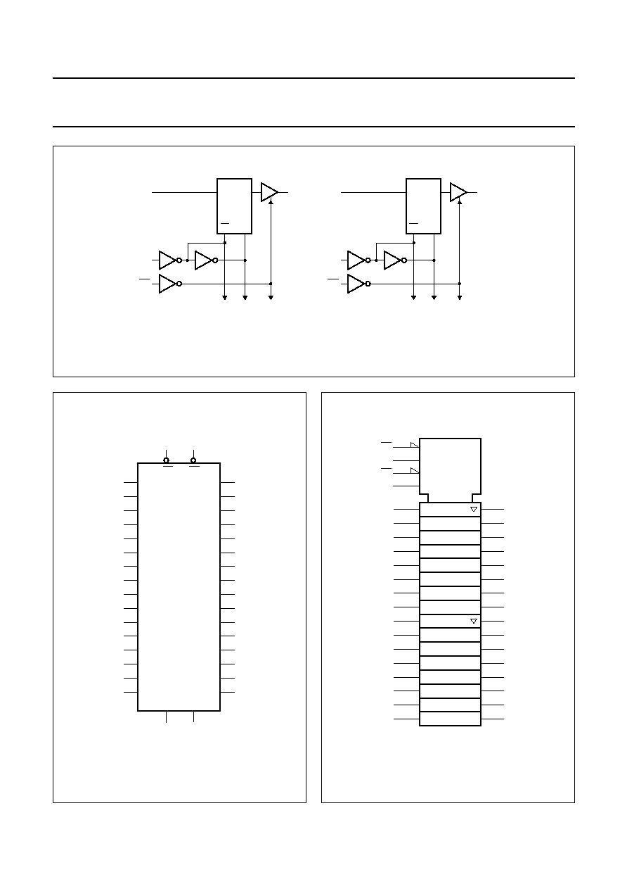
DESCRIPTION
The 74LVC(H)162373A is a 16-bit D-type transparent
latch featuring separate D-type inputs for each latch and
3-state outputs for bus oriented applications. One latch
enable (pin nLE) input and one output enable (pin nOE)
are provided for each octal. Inputs can be driven from
either 3.3 or 5 V devices. In 3-state operation, outputs can
handle 5 V. These features allow the use of these devices
in a mixed 3.3 and 5 V environment.
The 74LVC(H)162373A consists of 2 sections of eight
D-type transparent latches with 3-state true outputs. When
pin nLE is HIGH, data at the corresponding data inputs
(pins nDn) enter the latches. In this condition the latches
are transparent, i.e., a latch output will change each time
its corresponding data inputs changes.
When pin nLE is LOW the latches store the information
that was present at the data inputs a set-up time preceding
the HIGH-to-LOW transition of pin nLE. When pin nOE is
LOW, the contents of the eight latches are available at the
outputs. When pin nOE is HIGH, the outputs go to the
high-impedance OFF-state. Operation of the nOE input
does not affect the state of the latches.
The 74LVCH162373A bushold data inputs eliminates the
need for external pull-up resistors to hold unused inputs.
The 74LVC(H)162373A is designed with 30
series
termination resistors in both high and low output stages to
reduce line noise.
QUICK REFERENCE DATA
GND = 0 V; T
amb
= 25
°
C; t
r
= t
f
2.5 ns
Notes
1. C
PD
is used to determine the dynamic power dissipation (P
D
in
µ
W).
P
D
= C
PD
×
V
CC
2
×
f
i
×
N +
(C
L
×
V
CC
2
×
f
o
) where:
f
i
= input frequency in MHz;
f
o
= output frequency in MHz;
C
L
= output load capacitance in pF;
SYMBOL
PARAMETER
CONDITIONS
TYPICAL
UNIT
t
PHL
/t
PLH
propagation delay nDn to nQn
C
L
= 50 pF; V
CC
= 3.3 V
3.3
ns
propagation delay nLE to nQn
C
L
= 50 pF; V
CC
= 3.3 V
3.5
ns
t
PZH
/t
PZL
3-state output enable time nOE to nQn C
L
= 50 pF; V
CC
= 3.3 V
4.0
ns
t
PHZ
/t
PLZ
3-state output disable time nOE to nQn C
L
= 50 pF; V
CC
= 3.3 V
3.4
ns
C
I
input capacitance
5.0
pF
C
PD
power dissipation per latch
V
CC
= 3.3 V; notes 1 and 2
outputs enabled
26
pF
outputs disabled
19
pF
2004 Feb 05
3
Philips Semiconductors
Product specification
16-bit D-type transparent latch; 30
series termination
resistors; 5 V tolerant inputs/outputs; 3-state
74LVC162373A;
74LVCH162373A
V
CC
= supply voltage in Volts;
N = total load switching outputs;
(C
L
×
V
CC
2
×
f
o
) = sum of the outputs.
2. The condition is V
I
= GND to V
CC
.
ORDERING INFORMATION
FUNCTION TABLE
Per section of eight bits; note 1
Note
1. H = HIGH voltage level;
h = HIGH voltage level one set-up time prior to the HIGH-to-LOW LE transition;
L = LOW voltage level;
l = LOW voltage level one set-up time prior to the HIGH-to-LOW LE transition;
Z = high-impedance OFF-state.
TYPE NUMBER
TEMPERATURE
RANGE
PACKAGE
PINS
PACKAGE
MATERIAL
CODE
74LVC162373ADGG
-
40 to +125
°
C
48
TSSOP48
plastic
SOT362-1
74LVCH162373ADGG
-
40 to +125
°
C
48
TSSOP48
plastic
SOT362-1
74LVC162373ADL
-
40 to +125
°
C
48
SSOP48
plastic
SOT370-1
74LVCH162373ADL
-
40 to +125
°
C
48
SSOP48
plastic
SOT370-1
OPERATING MODES
INPUT
INTERNAL
LATCH
OUTPUT nQn
nOE
nLE
nDn
Enable and read register (transparent mode)
L
H
L
L
L
L
H
H
H
H
Latch and read register
L
L
l
L
L
L
L
h
H
H
Latch register and disable outputs
H
L
l
L
Z
H
L
h
H
Z
2004 Feb 05
4
Philips Semiconductors
Product specification
16-bit D-type transparent latch; 30
series termination
resistors; 5 V tolerant inputs/outputs; 3-state
74LVC162373A;
74LVCH162373A
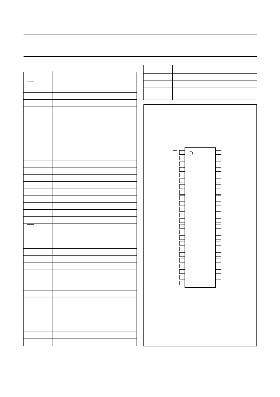
PINNING
SYMBOL
PIN
DESCRIPTION
1OE
1
output enable input
(active LOW)
1Q0
2
data output
1Q1
3
data output
GND
4, 10, 15, 21, 28,
34, 39, 45
ground (0 V)
1Q2
5
data output
1Q3
6
data output
V
CC
7, 18, 31, 42
supply voltage
1Q4
8
data output
1Q5
9
data output
1Q6
11
data output
1Q7
12
data output
2Q0
13
data output
2Q1
14
data output
2Q2
16
data output
2Q3
17
data output
2Q4
19
data output
2Q5
20
data output
2Q6
22
data output
2Q7
23
data output
2OE
24
output enable input
(active LOW)
2LE
25
latch enable input
(active HIGH)
2D7
26
data input
2D6
27
data input
2D5
29
data input
2D4
30
data input
2D3
32
data input
2D2
33
data input
2D1
35
data input
2D0
36
data input
1D7
37
data input
1D6
38
data input
1D5
40
data input
1D4
41
data input
1D3
43
data input
1D2
44
data input
1D1
46
data input
1D0
47
data input
1LE
48
latch enable input
(active HIGH)
SYMBOL
PIN
DESCRIPTION
162373A
001aaa336
1
2
3
4
5
6
7
8
9
10
11
12
13
14
15
16
17
18
19
20
21
22
23
24
48
47
46
45
44
43
42
41
40
39
38
37
36
35
34
33
32
31
30
29
28
27
26
25
1Q0
1Q1
GND
1Q2
1Q3
V
CC
1Q4
1Q5
GND
1Q6
1Q7
2Q0
2Q1
GND
2Q2
2Q3
V
CC
2Q4
2Q5
GND
2Q6
2Q7
2OE
1OE
1D0
1D1
GND
1D2
1D3
V
CC
1D4
1D5
GND
1D6
1D7
2D0
2D1
GND
2D2
2D3
V
CC
2D4
2D5
GND
2D6
2D7
2LE
1LE
Fig.1 Pin configuration SSOP48 and TSSOP48.