Äîêóìåíòàöèÿ è îïèñàíèÿ www.docs.chipfind.ru
Philips
Semiconductors
74LVC16373A/74LVCH16373A
16-bit D-type transparent latch with 5 Volt
tolerant inputs/outputs (3-State)
Product specification
Supersedes data of 1997 Aug 22
IC24 Data Handbook
1998 Mar 17
INTEGRATED CIRCUITS
Philips Semiconductors
Product specification
74LVC16373A/
74LVCH16373A
16-bit D-type transparent latch with 5 Volt tolerant
inputs/outputs (3-State)
2
1998 Mar 17
853-2027 19112
FEATURES
·
5 volt tolerant inputs/outputs for interfacing with 5V logic
·
Wide supply voltage range of 1.2V to 3.6V
·
Complies with JEDEC standard no. 8-1A
·
CMOS low power consumption
·
MULTIBYTE
TM
flow-through standard pin-out architecture
·
Low inductance multiple power and ground pins for minimum
noise and ground bounce
·
Direct interface with TTL levels
·
All data inputs have bus hold (74LVCH167373A only)
·
High impedance when V
CC
= 0
DESCRIPTION
The 74LVC(H)16373A is a 16-bit D-type transparent latch featuring
separate D-type inputs for each latch and 3-State outputs for bus
oriented applications. One latch enable (LE) input and one output
enable (OE) are provided for each octal. Inputs can be driven from
either 3.3V or 5V devices. In 3-State operation, outputs can handle
5V. These features allow the use of these devices in a mixed
3.3V/5V environment.
The 74LVC(H)16373A consists of 2 sections of eight D-type
transparent latches with 3-State true outputs. When LE is HIGH,
data at the Dn inputs enter the latches. In this condition the latches
are transparent, i.e., a latch output will change each time its
corresponding D-input changes.
When LE is LOW the latches store the information that was present
at the D-inputs a set-up time preceding the HIGH-to-LOW transition
of LE. When OE is LOW, the contents of the eight latches are
available at the outputs. When OE is HIGH, the outputs go to the
high impedance OFF-state. Operation of the OE input does not
affect the state of the latches.
The 74LVCH16373A bus hold data inputs eliminates the need for
external pull up resistors to hold unused inputs.
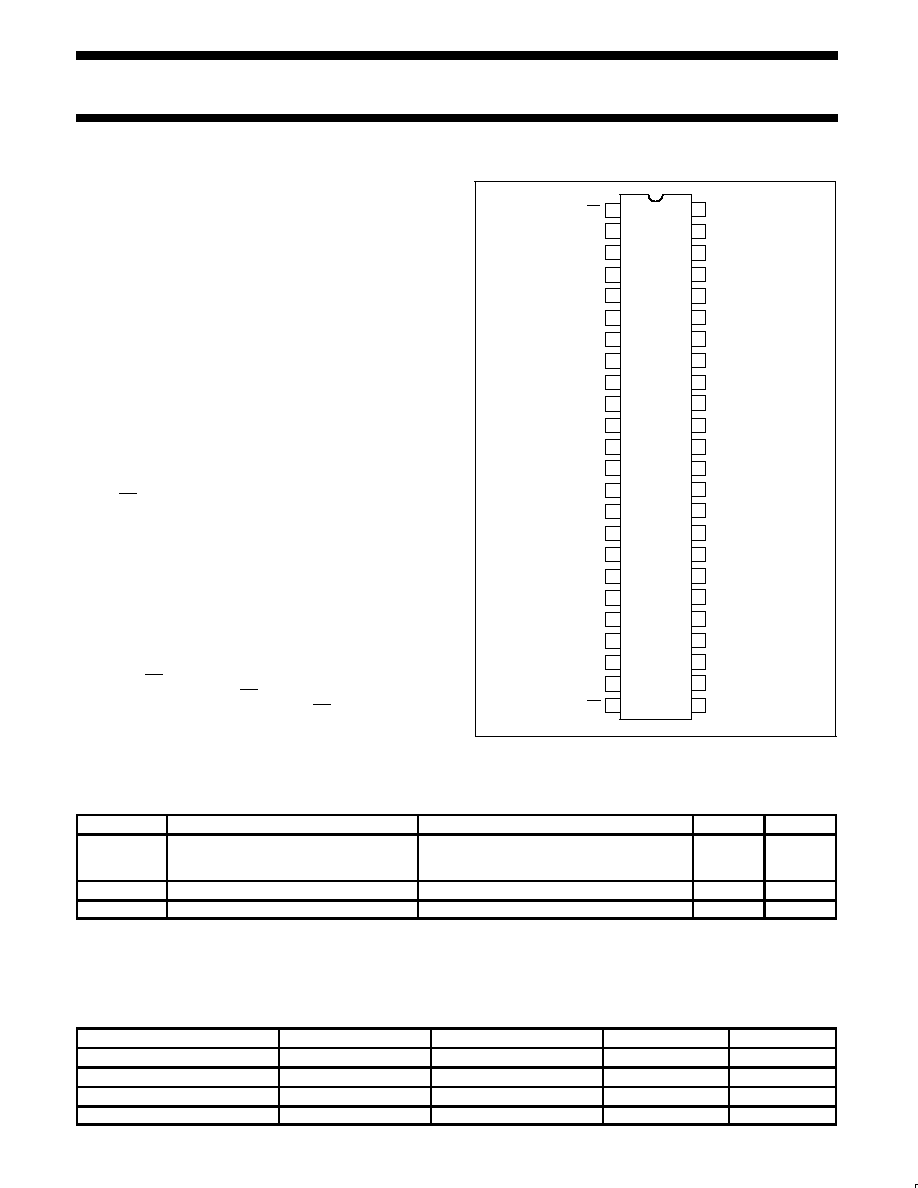
PIN CONFIGURATION
1
2
3
4
5
6
7
8
9
10
11
12
13
14
15
16
17
18
19
20
29
30
31
32
33
34
35
36
37
38
39
40
41
42
43
44
45
46
47
48
1OE
1Q0
1Q1
GND
1Q2
1Q3
V
CC
1Q5
GND
1Q6
1Q7
2Q0
2Q1
GND
1Q4
2Q2
2Q3
V
CC
2Q4
2Q5
2D5
2D4
V
CC
2D3
2D2
GND
2D1
2D0
1D7
1D6
GND
1D5
1D4
V
CC
1D3
1D2
GND
1D1
1D0
1LE
21
22
23
24
25
26
27
28
GND
2Q6
2Q7
2OE
2LE
2D7
2D6
GND
SW00066
QUICK REFERENCE DATA
GND = 0V; T
amb
= 25
°
C; t
r
= t
f
2.5ns
SYMBOL
PARAMETER
CONDITIONS
TYPICAL
UNIT
t
PHL
/t
PLH
Propagation delay
Dn to Qn
LE to Qn
C
L
= 50pF
V
CC
= 3.3V
3.0
3.4
ns
C
I
Input capacitance
5.0
pF
C
PD
Power dissipation capacitance per latch
V
CC
= 3.3V
26
pF
NOTES:
1. C
PD
is used to determine the dynamic power dissipation (P
D
in
µ
W):
P
D
= C
PD
×
V
CC
2
×
f
i
+
S
(C
L
×
V
CC
2
×
f
o
) where:
f
i
= input frequency in MHz; C
L
= output load capacity in pF;
f
o
= output frequency in MHz; V
CC
= supply voltage in V;
S
(C
L
×
V
CC
2
×
f
o
) = sum of outputs.
ORDERING INFORMATION
PACKAGES
TEMPERATURE RANGE
OUTSIDE NORTH AMERICA
NORTH AMERICA
DWG NUMBER
48-Pin Plastic SSOP Type III
40
°
C to +85
°
C
74LVC16373A DL
VC16373A DL
SOT370-1
48-Pin Plastic TSSOP Type II
40
°
C to +85
°
C
74LVC16373A DGG
VC16373A DGG
SOT362-1
48-Pin Plastic SSOP Type III
40
°
C to +85
°
C
74LVCH16373A DL
VCH16373A DL
SOT370-1
48-Pin Plastic TSSOP Type II
40
°
C to +85
°
C
74LVCH16373A DGG
VCH16373A DGG
SOT362-1
Philips Semiconductors
Product specification
74LVC16373A/
74LVCH16373A
16-bit D-type transparent latch with 5 Volt tolerant
inputs/outputs (3-State)
1998 Mar 17
3
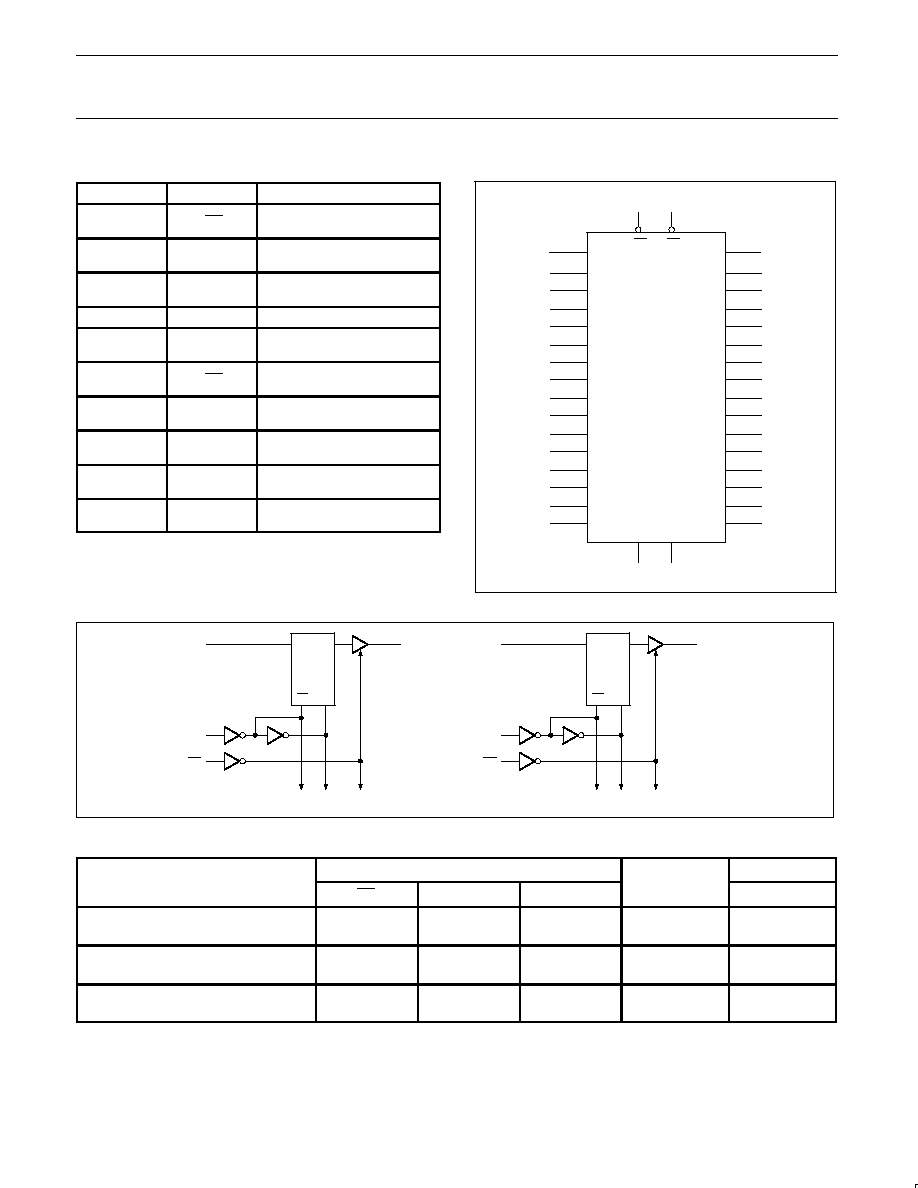
PIN DESCRIPTION
PIN NUMBER
SYMBOL
NAME AND FUNCTION
1
1OE
Output enable input
(active LOW)
2, 3, 5, 6, 8, 9,
11, 12
1Q0 to 1Q7
Data inputs/outputs
4, 10, 15, 21,
28, 34, 39, 45
GND
Ground (0V)
7, 18, 31, 42
V
CC
Positive supply voltage
13, 14, 16, 17,
19, 20, 22, 23
2Q0 to 2Q7
Data inputs/outputs
24
2OE
Output enable input
(active LOW)
25
2LE
Latch enable input (active
HIGH)
36, 35, 33, 32,
30, 29, 27, 26
2D0 to 2D7
Data inputs
47, 46, 44, 43,
41, 40, 38, 37
1D0 to 1D7
Data inputs
48
1LE
Latch enable input (active
HIGH)
LOGIC SYMBOL
1OE
2OE
1LE
2LE
1D0
1D1
1D2
1D3
1D4
1D5
1D6
1D7
2D0
2D1
2D2
2D3
2D4
2D5
2D6
2D7
1Q0
1Q1
1Q2
1Q3
1Q4
1Q5
1Q6
1Q7
2Q0
2Q1
2Q2
2Q3
2Q4
2Q5
2Q6
2Q7
47
46
44
43
41
40
38
37
36
35
33
32
30
29
27
26
48
25
23
22
20
19
17
16
14
13
12
11
9
8
6
5
3
2
24
1
SW00067
LOGIC DIAGRAM
D
Q
LE
LE
LATCH
1
1D0
1LE
1OE
1Q0
TO 7 OTHER CHANNELS
D
Q
LE
LE
LATCH
9
2D0
2LE
2OE
2Q0
TO 7 OTHER CHANNELS
SW00068
FUNCTION TABLE (per section of eight bits)
OPERATING MODES
INPUTS
INTERNAL
OUTPUTS
OPERATING MODES
OE
LE
Dn
LATCHES
Q0 to Q7
enable and read register
(transparent mode)
L
L
H
H
L
H
L
H
L
H
latch and read register
L
L
L
L
l
h
L
H
L
H
latch register and disable outputs
H
H
L
L
l
h
L
H
Z
Z
H = HIGH voltage level
h
= HIGH voltage level one set-up time prior to the HIGH-to-LOW LE transition
L
= LOW voltage level
l
= LOW voltage level one set-up time prior to the HIGH-to-LOW LE transition
X = don't care
Z = high impedance OFF-state
Philips Semiconductors
Product specification
74LVC16373A/
74LVCH16373A
16-bit D-type transparent latch with 5 Volt tolerant
inputs/outputs (3-State)
1998 Mar 17
4
LOGIC SYMBOL (IEEE/IEC)
SW00069
48
1EN
1
46
44
43
41
40
38
37
36
C3
C4
2EN
2
4D
1
25
24
47
35
33
32
30
29
27
26
3
2
5
6
8
9
11
12
13
14
16
17
19
20
22
23
1OE
1LE
1D0
1D1
1D2
1D3
1D4
1D5
1D6
2D0
2D1
2D2
2D3
2D4
2D5
2D6
2D7
1Q0
1Q1
1Q2
1Q3
1Q4
1Q5
1Q6
1Q7
2Q0
2Q1
2Q2
2Q3
2Q4
2Q7
1D7
2Q5
2Q6
3D
2OE
2LE
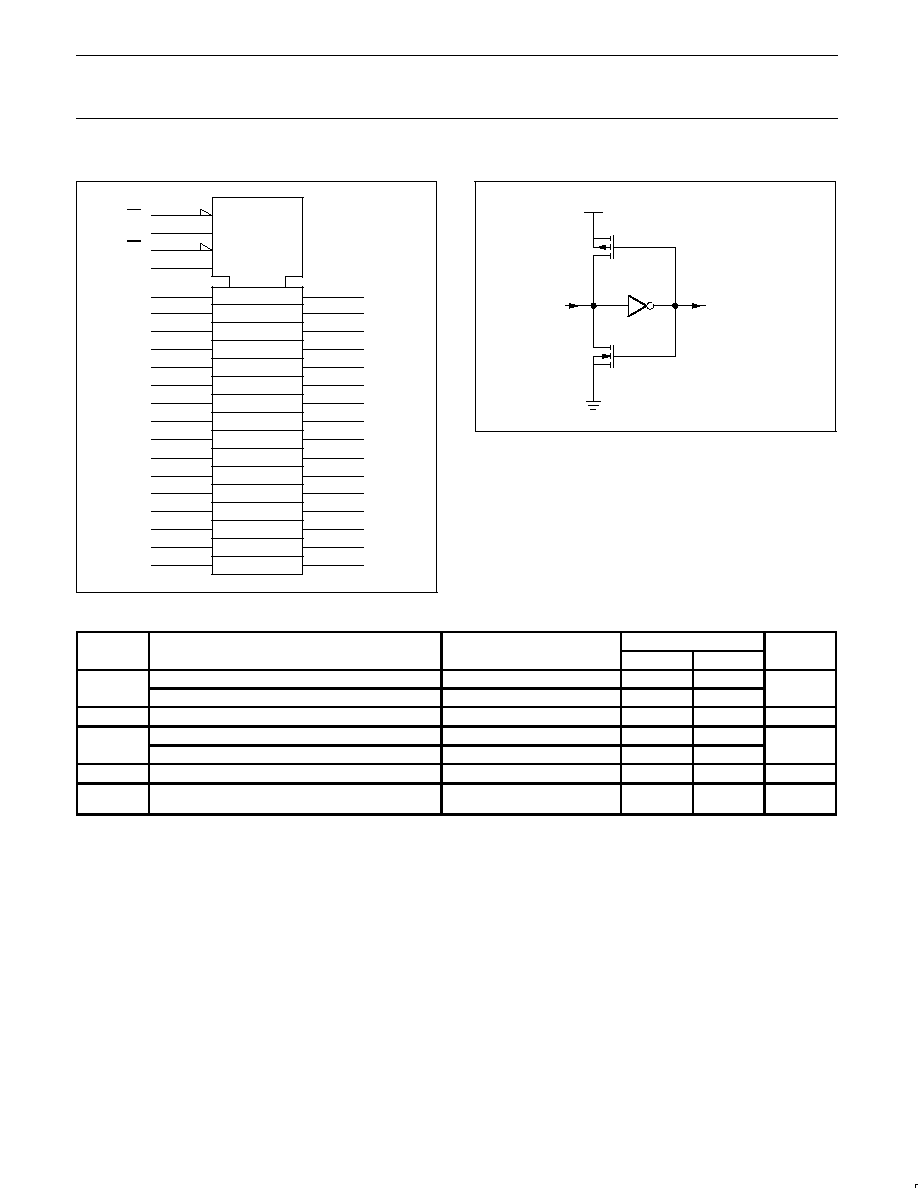
BUS HOLD CIRCUIT
To internal circuit
V
CC
Data Input
SW00044
RECOMMENDED OPERATING CONDITIONS
SYMBOL
PARAMETER
CONDITIONS
LIMITS
UNIT
SYMBOL
PARAMETER
CONDITIONS
MIN
MAX
UNIT
V
CC
DC supply voltage (for max. speed performance)
2.7
3.6
V
V
CC
DC supply voltage (for low-voltage applications)
1.2
3.6
V
V
I
DC input voltage range
0
5.5
V
V
O
DC input voltage range; output HIGH or LOW state
0
V
CC
V
V
O
DC output voltage range; output 3-State
0
5.5
V
T
amb
Operating free-air temperature range
40
+85
°
C
t
r
, t
f
Input rise and fall times
V
CC
= 1.2 to 2.7V
V
CC
= 2.7 to 3.6V
0
0
20
10
ns/V
Philips Semiconductors
Product specification
74LVC16373A/
74LVCH16373A
16-bit D-type transparent latch with 5 Volt tolerant
inputs/outputs (3-State)
1998 Mar 17
5
ABSOLUTE MAXIMUM RATINGS
1
In accordance with the Absolute Maximum Rating System (IEC 134).
Voltages are referenced to GND (ground = 0 V).
SYMBOL
PARAMETER
CONDITIONS
RATING
UNIT
V
CC
DC supply voltage
0.5 to +6.5
V
I
IK
DC input diode current
V
I
t
0
50
mA
V
I
DC input voltage
Note 2
0.5 to +6.5
V
I
OK
DC output diode current
V
O
u
V
CC
or V
O
t
0
"
50
mA
V
O
DC output voltage; output HIGH or LOW state
Note 2
0.5 to V
CC
+0.5
V
V
O
DC output voltage; output 3-State
Note 2
0.5 to 6.5
V
I
O
DC output source or sink current
V
O
= 0 to V
CC
"
50
mA
I
GND
, I
CC
DC V
CC
or GND current
"
100
mA
T
stg
Storage temperature range
65 to +150
°
C
Power dissipation per package
P
TOT
plastic mini-pack (SO)
above +70
°
C derate linearly with 8 mW/K
500
mW
plastic shrink mini-pack (SSOP and TSSOP)
above +60
°
C derate linearly with 5.5 mW/K
500
mW
NOTES:
1. Stresses beyond those listed may cause permanent damage to the device. These are stress ratings only and functional operation of the
device at these or any other conditions beyond those indicated under "recommended operating conditions" is not implied. Exposure to
absolute-maximum-rated conditions for extended periods may affect device reliability.
2. The input and output voltage ratings may be exceeded if the input and output current ratings are observed.
DC ELECTRICAL CHARACTERISTICS
Over recommended operating conditions voltages are referenced to GND (ground = 0V)
LIMITS
SYMBOL
PARAMETER
TEST CONDITIONS
Temp = -40
°
C to +85
°
C
UNIT
MIN
TYP
1
MAX
V
IH
HIGH level Input voltage
V
CC
= 1.2V
V
CC
V
V
IH
HIGH level In ut voltage
V
CC
= 2.7 to 3.6V
2.0
V
V
IL
LOW level Input voltage
V
CC
= 1.2V
GND
V
V
IL
LOW level In ut voltage
V
CC
= 2.7 to 3.6V
0.8
V
V
CC
= 2.7V; V
I
= V
IH
or V
IL
; I
O
= 12mA
V
CC
*
0.5
V
V
= 3 0V; V = V
or V ; I = 100
µ
A
V
0 2
V
V
O
HIGH level output voltage
V
CC
= 3.0V; V
I
= V
IH
or V
IL
; I
O
= 100
µ
A
V
CC
*
0.2
V
CC
V
OH
HIGH level output voltage
V
CC
= 3.0V; V
I
= V
IH
or V
IL;
I
O
= 18mA
V
CC
*
0.6
V
V
CC
= 3.0V; V
I
= V
IH
or V
IL;
I
O
= 24mA
V
CC
*
0.8
V
CC
= 2.7V; V
I
= V
IH
or V
IL
; I
O
= 12mA
0.40
V
OL
LOW level output voltage
V
CC
= 3.0V; V
I
= V
IH
or V
IL
; I
O
= 100
µ
A
0.20
V
V
CC
= 3.0V; V
I
= V
IH
or V
IL;
I
O
= 24mA
0.55
I
I
Input leakage current
V
CC
= 3.6V; V
I
= 5.5V or GND
6
"
0.1
"
5
µ
A
I
OZ
3-State output OFF-state current
V
CC
= 3.6V; V
I
= V
IH
or V
IL
; V
O
= 5.5V or GND
0.1
"
5
µ
A
I
off
Power off leakage supply
V
CC
= 0.0V; V
I
or V
O
= 5.5V
"
10
µ
A
I
CC
Quiescent supply current
V
CC
= 3.6V; V
I
= V
CC
or GND; I
O
= 0
0.1
20
µ
A
I
CC
Additional quiescent supply
current per input pin
V
CC
= 2.7V to 3.6V; V
I
= V
CC
0.6V; I
O
= 0
5
500
µ
A