2002 Oct 02
2
Philips Semiconductors
Product specification
Single inverter
74LVC1G04
FEATURES
∑
Wide supply voltage range from 1.65 to 5.5 V
∑
High noise immunity
∑
Complies with JEDEC standard:
≠ JESD8-7 (1.65 to 1.95 V)
≠ JESD8-5 (2.3 to 2.7 V)
≠ JESD8B/JESD36 (2.7 to 3.6 V).
∑ ±
24 mA output drive (V
CC
= 3.0 V)
∑
CMOS low power consumption
∑
Latch-up performance
250 mA
∑
Direct interface with TTL levels
∑
Inputs accept voltages up to 5 V
∑
Multiple package options
∑
Specified from
-
40 to +125
∞
C.
DESCRIPTION
The 74LVC1G04 is a high-performance, low-power,
low-voltage, Si-gate CMOS device, superior to most
advanced CMOS compatible TTL families.
Input can be driven from either 3.3 or 5 V devices. These
features allow the use of these devices in a mixed
3.3 and 5 V environment.
Schmitt trigger action at all inputs makes the circuit tolerant
for slower input rise and fall time.
This device is fully specified for partial power-down
applications using I
off
. The I
off
circuitry disables the output,
preventing the damaging backflow current through the
device when it is powered down.
The 74LVC1G04 provides the inverting buffer.
QUICK REFERENCE DATA
GND = 0 V; T
amb
= 25
∞
C; t
r
= t
f
2.5 ns.
Notes
1. C
PD
is used to determine the dynamic power dissipation (P
D
in
µ
W).
P
D
= C
PD
◊
V
CC
2
◊
f
i
+ (C
L
◊
V
CC
2
◊
f
o
) where:
f
i
= input frequency in MHz;
f
o
= output frequency in MHz;
C
L
= output load capacitance in pF;
V
CC
= supply voltage in Volts.
2. The condition is V
I
= GND to V
CC
.
SYMBOL
PARAMETER
CONDITIONS
TYPICAL
UNIT
t
PHL
/t
PLH
propagation delay input A to output Y
V
CC
= 1.8 V; C
L
= 30 pF; R
L
= 1 k
3
ns
V
CC
= 2.5 V; C
L
= 30 pF; R
L
= 500
2
ns
V
CC
= 2.7 V; C
L
= 50 pF; R
L
= 500
2.3
ns
V
CC
= 3.3 V; C
L
= 50 pF; R
L
= 500
2
ns
V
CC
= 5.0 V; C
L
= 50 pF; R
L
= 500
1.6
ns
C
I
input capacitance
5
pF
C
PD
power dissipation capacitance per buffer
V
CC
= 3.3 V; notes 1 and 2
14
pF
2002 Oct 02
4
Philips Semiconductors
Product specification
Single inverter
74LVC1G04
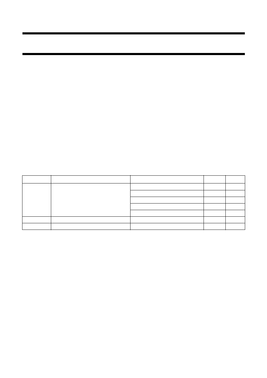
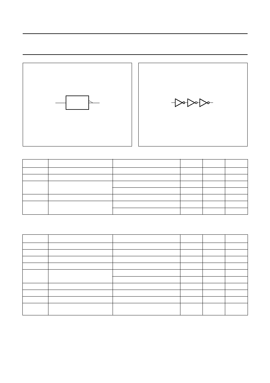
handbook, halfpage
MNA109
4
1
2
Fig.3 IEE/IEC logic symbol.
handbook, halfpage
MNA110
A
Y
Fig.4 Logic diagram.
RECOMMENDED OPERATING CONDITIONS
LIMITING VALUES
In accordance with the Absolute Maximum Rating System (IEC 60134); voltages are referenced to GND (ground = 0 V).
Notes
1. The input and output voltage ratings may be exceeded if the input and output current ratings are observed.
2. When V
CC
= 0 V (Power-down mode), the output voltage can be 5.5 V in normal operation.
SYMBOL
PARAMETER
CONDITIONS
MIN.
MAX.
UNIT
V
CC
supply voltage
1.65
5.5
V
V
I
input voltage
0
5.5
V
V
O
output voltage
active mode
0
V
CC
V
V
CC
= 0 V; Power-down mode
0
5.5
V
T
amb
operating ambient temperature
-
40
+125
∞
C
t
r
, t
f
input rise and fall times
V
CC
= 1.65 to 2.7 V
0
20
ns/V
V
CC
= 2.7 to 5.5 V
0
10
ns/V
SYMBOL
PARAMETER
CONDITIONS
MIN.
MAX.
UNIT
V
CC
supply voltage
-
0.5
+6.5
V
I
IK
input diode current
V
I
< 0
-
-
50
mA
V
I
input voltage
note 1
-
0.5
+6.5
V
I
OK
output diode current
V
O
> V
CC
or V
O
< 0
-
±
50
mA
V
O
output voltage
active mode; notes 1 and 2
-
0.5
V
CC
+ 0.5
V
Power-down mode; notes 1 and 2
-
0.5
+6.5
V
I
O
output source or sink current
V
O
= 0 to V
CC
-
±
50
mA
I
CC
, I
GND
V
CC
or GND current
-
±
100
mA
T
stg
storage temperature
-
65
+150
∞
C
P
D
power dissipation per package
for temperature range from
-
40 to +125
∞
C
-
250
mW