Äîêóìåíòàöèÿ è îïèñàíèÿ www.docs.chipfind.ru

9397 750 12675
© Koninklijke Philips Electronics N.V. 2004. All rights reserved.
Product data sheet
Rev. 01 -- 26 February 2004
1 of 22
Philips Semiconductors
74LVC1G384
Bilateral switch
1.
General description
The 74LVC1G384 is a high-speed Si-gate CMOS device.
The 74LVC1G384 provides an analog switch. The switch has input and output terminals
(pins Y and Z) and an active LOW enable input (pin E). When pin E is HIGH, the analog
switch is turned off.
2.
Features
s
Very low ON-resistance:
x
7.5
(typ) at V
CC
= 2.7 V
x
6.5
(typ) at V
CC
= 3.3 V
x
6.0
(typ) at V
CC
= 5 V.
s
ESD protection:
x
HBM EIA/JESD22-A114-A exceeds 2 000 V
x
MM EIA/JESD22-A115-A exceeds 200 V.
s
High noise immunity
s
CMOS low power consumption
s
Direct interface TTL-levels
s
Latch-up performance meets requirements of JESD78 Class I
s
Multiple package options
s
Specified from
-
40
°
C to +80
°
C and
-
40
°
C to +125
°
C.
3.
Quick reference data
74LVC1G384
Bilateral switch
Rev. 01 -- 26 February 2004
Product data sheet
Table 1:
Quick reference data
Ground = 0 V; T
amb
= 25
°
C; t
r
= t
f
3.0 ns.
Symbol
Parameter
Conditions
Min
Typ
Max
Unit
t
PZH
, t
PZL
turn-on time E to Y or Z
C
L
= 50 pF; R
L
= 500
V
CC
= 3.3 V
-
4.8
-
ns
V
CC
= 5.0 V
-
3.3
-
ns
t
PHZ
, t
PLZ
turn-off time E to Y or Z
C
L
= 50 pF; R
L
= 500
V
CC
= 3.3 V
-
5.4
-
ns
V
CC
= 5.0 V
-
3.6
-
ns
C
I
input capacitance
-
2
-
pF
9397 750 12675
© Koninklijke Philips Electronics N.V. 2004. All rights reserved.
Product data sheet
Rev. 01 -- 26 February 2004
2 of 22
Philips Semiconductors
74LVC1G384
Bilateral switch
[1]
C
PD
is used to determine the dynamic power dissipation (P
D
in
µ
W).
P
D
= C
PD
×
V
CC
2
×
f
i
+ (C
L
+ C
S
)
×
V
CC
2
×
f
o
where:
f
i
= input frequency in MHz;
f
o
= output frequency in MHz;
C
L
= output load capacitance in pF;
C
S
= maximum switch capacitance in pF;
V
CC
= supply voltage in V.
[2]
The condition is V
I
= GND to V
CC
.
4.
Ordering information
5.
Marking
6.
Functional diagram
C
PD
power dissipation
capacitance
C
L
= 50 pF; f
i
= 10 MHz;
V
CC
= 3.3 V
[1]
[2]
-
15.2
-
pF
C
S
switch capacitance
OFF-state
-
5
-
pF
ON-state
-
9.5
-
pF
Table 1:
Quick reference data
...continued
Ground = 0 V; T
amb
= 25
°
C; t
r
= t
f
3.0 ns.
Symbol
Parameter
Conditions
Min
Typ
Max
Unit
Table 2:
Ordering information
Type number
Package
Temperature range Name
Description
Version
74LVC1G384GW
-
40
°
C to +125
°
C
-
plastic surface mounted package; 5 leads
SOT353
74LVC1G384GV
-
40
°
C to +125
°
C
-
plastic surface mounted package; 5 leads
SOT753
Table 3:
Marking
Type number
Marking code
74LVC1G384GW
YL
74LVC1G384GV
YL
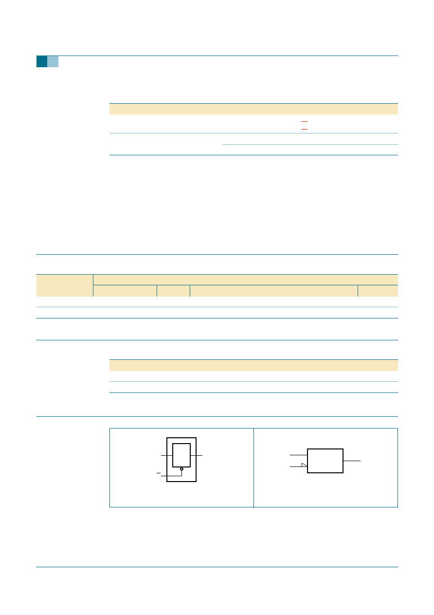
Fig 1.
Logic symbol.
Fig 2.
IEC logic symbol.
001aaa374
Z
Y
E
001aaa373
2
4 #
1
X1
1
1
9397 750 12675
© Koninklijke Philips Electronics N.V. 2004. All rights reserved.
Product data sheet
Rev. 01 -- 26 February 2004
3 of 22
Philips Semiconductors
74LVC1G384
Bilateral switch
7.
Pinning information
7.1 Pinning
7.2 Pin description
8.
Functional description
8.1 Function table
[1]
H = HIGH voltage level;
L = LOW voltage level.
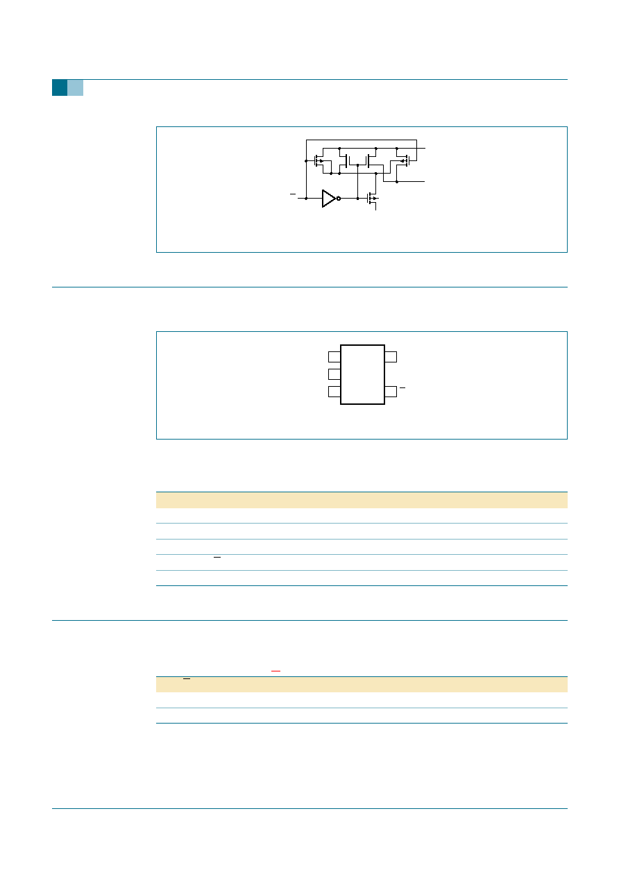
Fig 3.
Logic diagram.
001aaa372
Y
V
CC
Z
E
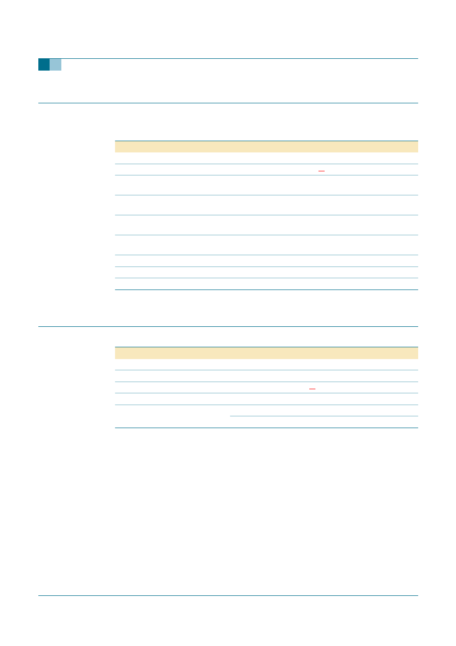
Fig 4.
Pin configuration.
1
2
3
5
4
001aaa365
384
VCC
Z
E
GND
Y
Table 4:
Pin description
Pin
Symbol
Description
1
Y
independent input or output
2
Z
independent output or input
3
GND
ground (0 V)
4
E
enable input (active LOW)
5
V
CC
supply voltage
Table 5:
Function table
[1]
Input E
Switch
L
ON-state
H
OFF-state
9397 750 12675
© Koninklijke Philips Electronics N.V. 2004. All rights reserved.
Product data sheet
Rev. 01 -- 26 February 2004
4 of 22
Philips Semiconductors
74LVC1G384
Bilateral switch
9.
Limiting values
[1]
The input and output voltage ratings may be exceeded if the input and output current ratings are observed.
10. Recommended operating conditions
[1]
To avoid drawing V
CC
current out of terminal Z, when switch current flows in terminal Y, the voltage drop
across the bidirectional switch must not exceed 0.4 V. If the switch current flows into terminal Z, no V
CC
current will flow out of terminal Y. In this case there is no limit for the voltage drop across the switch.
Table 6:
Limiting values
In accordance with the Absolute Maximum Rating System (IEC 60134). Voltages are referenced to
GND (ground = 0 V).
Symbol
Parameter
Conditions
Min
Max
Unit
V
CC
supply voltage
-
0.5
+6.5
V
V
I
input voltage
[1]
-
0.5
+6.5
V
I
IK
input diode current
V
I
<
-
0.5 V or
V
I
> V
CC
+ 0.5 V
-
-
50
mA
I
SK
switch diode current
V
I
<
-
0.5 V or
V
I
> V
CC
+ 0.5 V
-
±
50
mA
V
S
DC switch voltage
range
enable and disable mode
-
0.5
V
CC
+ 0.5
V
I
S
DC switch source or
sink current
V
S
>
-
0.5 V or
V
S
< V
CC
+ 0.5 V
-
±
50
mA
I
CC
, I
GND
V
CC
or GND current
-
±
100
mA
T
stg
storage temperature
-
65
+150
°
C
P
tot
power dissipation
T
amb
=
-
40
°
C to +125
°
C
-
250
mW
Table 7:
Recommended operating conditions
Symbol
Parameter
Conditions
Min
Typ
Max
Unit
V
CC
supply voltage
1.65
-
5.5
V
V
I
input voltage
0
-
5.5
V
V
S
DC switch voltage range
[1]
0
-
V
CC
V
T
amb
ambient temperature
-
40
-
+125
°
C
t
r
, t
f
input rise and fall times
V
CC
= 1.65 V to 2.7 V
0
-
20
ns/V
V
CC
= 2.7 V to 5.5 V
0
-
10
ns/V
9397 750 12675
© Koninklijke Philips Electronics N.V. 2004. All rights reserved.
Product data sheet
Rev. 01 -- 26 February 2004
5 of 22
Philips Semiconductors
74LVC1G384
Bilateral switch
11. Static characteristics
Table 8:
Static characteristics
At recommended operating conditions; voltages are referenced to GND (ground = 0 V).
Symbol
Parameter
Conditions
Min
Typ
Max
Unit
T
amb
=
-
40
°
C to +85
°
C
[1]
V
IH
HIGH-level input
voltage
V
CC
= 1.65 V to 1.95 V
0.65
×
V
CC
-
-
V
V
CC
= 2.3 V to 2.7 V
1.7
-
-
V
V
CC
= 2.7 V to 3.6 V
2.0
-
-
V
V
CC
= 4.5 V to 5.5 V
0.7
×
V
CC
-
-
V
V
IL
LOW-level input
voltage
V
CC
= 1.65 V to 1.95 V
-
-
0.35
×
V
CC
V
V
CC
= 2.3 V to 2.7 V
-
-
0.7
V
V
CC
= 2.7 V to 3.6 V
-
-
0.8
V
V
CC
= 4.5 V to 5.5 V
-
-
0.3
×
V
CC
V
I
LI
input leakage current
on control pin
V
I
= 5.5 V or GND; V
CC
= 5.5 V
[2]
-
±
0.1
±
5
µ
A
I
S(OFF)
analog switch
OFF-state current
V
I
= V
IH
or V
IL
; |V
S
| = V
CC
-
GND;
V
CC
= 5.5 V; see
Figure 5
[2]
-
±
0.1
±
5
µ
A
I
S(ON)
analog switch
ON-state current
V
I
= V
IH
or V
IL
; |V
S
| = V
CC
-
GND;
V
CC
= 5.5 V; see
Figure 6
[2]
-
±
0.1
±
5
µ
A
I
CC
quiescent supply
current
V
I
= V
CC
or GND; V
S
= GND or V
CC
;
I
O
= 0 A; V
CC
= 5.5 V
[2]
-
0.1
10
µ
A
I
CC
additional quiescent
supply current per
control pin
V
I
= V
CC
-
0.6 V; V
S
= GND or V
CC
;
I
O
= 0 A; V
CC
= 5.5 V
[2]
-
5
500
µ
A
C
I
input capacitance
-
2
-
pF
R
ON(peak)
switch ON-state
resistance (peak)
V
I
= GND to V
CC
; see
Figure 7
and
Figure 8
I
S
= 4 mA; V
CC
= 1.65 V to 1.95 V
-
35
130
I
S
= 8 mA; V
CC
= 2.3 V to 2.7 V
-
14
30
I
S
= 12 mA; V
CC
= 2.7 V
-
11.5
25
I
S
= 24 mA; V
CC
= 3.0 V to 3.6 V
-
8.5
20
I
S
= 32 mA; V
CC
= 4.5 V to 5.5 V
-
6.5
15
R
ON(rail)
switch ON-state
resistance rail
V
I
= GND
I
S
= 4 mA; V
CC
= 1.65 V to 1.95 V
-
10
30
I
S
= 8 mA; V
CC
= 2.3 V to 2.7 V
-
8.5
20
I
S
= 12 mA; V
CC
= 2.7 V
-
7.5
18
I
S
= 24 mA; V
CC
= 3.0 V to 3.6 V
-
6.5
15
I
S
= 32 mA; V
CC
= 4.5 V to 5.5 V
-
6
10
V
I
= V
CC
I
S
= 4 mA; V
CC
= 1.65 V to 1.95 V
-
12
30
I
S
= 8 mA; V
CC
= 2.3 V to 2.7 V
-
8.5
20
I
S
= 12 mA; V
CC
= 2.7 V
-
7.5
18
I
S
= 24 mA; V
CC
= 3.0 V to 3.6 V
-
6.5
15
I
S
= 32 mA; V
CC
= 4.5 V to 5.5 V
-
6
10
Document Outline