 | ÐлекÑÑоннÑй компоненÑ: 74LVC240 | СкаÑаÑÑ:  PDF PDF  ZIP ZIP |
Äîêóìåíòàöèÿ è îïèñàíèÿ www.docs.chipfind.ru
Philips
Semiconductors
74LVC240A
Octal buffer/line driver with 5-volt tolerant
inputs/outputs; inverting (3-State)
Product specification
IC24 Data Handbook
1998 May 20
INTEGRATED CIRCUITS
Philips Semiconductors
Product specification
74LVC240A
Octal buffer/line driver with 5-volt
tolerant inputs/outputs; inverting (3-State)
2
1998 May 20
853-1981 19419
FEATURES
·
5-volt tolerant inputs/outputs, for interfacing with 5-volt logic
·
Supply voltage range of 1.2V to 3.6V
·
Complies with JEDEC standard no. 8-1A
·
CMOS low power consumption
·
Direct interface with TTL levels
·
High impedance when V
CC
= 0V
DESCRIPTION
The 74LVC240A is a high-performance, low-power, low-voltage,
Si-gate CMOS device, superior to most advanced CMOS
compatible TTL families.
Inputs can be driven from either 3.3V or 5V devices. In 3-State
operation, outputs can handle 5V. These features allow the use of
these devices as translators in a mixed 3.3V/5V environment.
The `240A is an octal non-inverting buffer/line driver with 3-State
outputs. The 3-State outputs are controlled by the output enable
inputs 1OE and 2OE. A HIGH on nOE causes the outputs to
assume a high impedance OFF-state. Schmitt-trigger action at all
inputs makes the circuit highly tolerant for slower input rise and fall
times.
The '240' is functionally identical to the '244', but the '244' has
inverting outputs.
QUICK REFERENCE DATA
GND = 0 V; T
amb
= 25
°
C; t
r
= t
f
v
2.5 ns
SYMBOL
PARAMETER
CONDITIONS
TYPICAL
UNIT
t
PHL
/t
PLH
Propagation delay
1A
n
to 1Y
n;
2A
n
to 2Y
n
C
L
= 50pF
V
CC
= 3.3V
3.5
ns
C
I
Input capacitance
5.0
pF
C
PD
Power dissipation capacitance per
buffer
Notes 1 and 2
20
pF
NOTE:
1. C
PD
is used to determine the dynamic power dissipation (P
D
in
m
W):
P
D
= C
PD
x V
CC
2
x f
i
+
S
(C
L
x V
CC
2
x f
o
) where:
f
i
= input frequency in MHz; C
L
= output load capacity in pF;
f
o
= output frequency in MHz; V
CC
= supply voltage in V;
S
(C
L
x V
CC
2
x f
o
) = sum of outputs.
2. The condition is V
I
= GND to V
CC
ORDERING INFORMATION
PACKAGES
TEMPERATURE
RANGE
OUTSIDE
NORTH AMERICA
NORTH AMERICA
PKG. DWG. #
20-Pin Plastic Small Outline (SO)
40
°
C to +85
°
C
74LVC240A D
74LVC240A D
SOT163-1
20-Pin Plastic Shrink Small Outline (SSOP) Type II
40
°
C to +85
°
C
74LVC240A DB
74LVC240A DB
SOT339-1
20-Pin Plastic Thin Shrink Small Outline (TSSOP) Type I
40
°
C to +85
°
C
74LVC240A PW
7LVC240APW DH
SOT360-1
Philips Semiconductors
Product specification
74LVC240A
Octal buffer/line driver with 5-volt
tolerant inputs/outputs; inverting (3-State)
1998 May 20
3
PIN DESCRIPTION
PIN NUMBER
SYMBOL
FUNCTION
1
1OE
Output enable input (active LOW)
2, 4, 6, 8
1A
0
to 1A
3
Data inputs
3, 5, 7, 9
2Y
0
to 2Y
3
Bus outputs
10
GND
Ground (0V)
17, 15, 13, 11
2A
0
to 2A
3
Bus inputs
18, 16, 14, 12
1Y
0
to 1Y
3
Bus outputs
19
2OE
Output enable input (active-LOW)
20
V
CC
Positive power supply
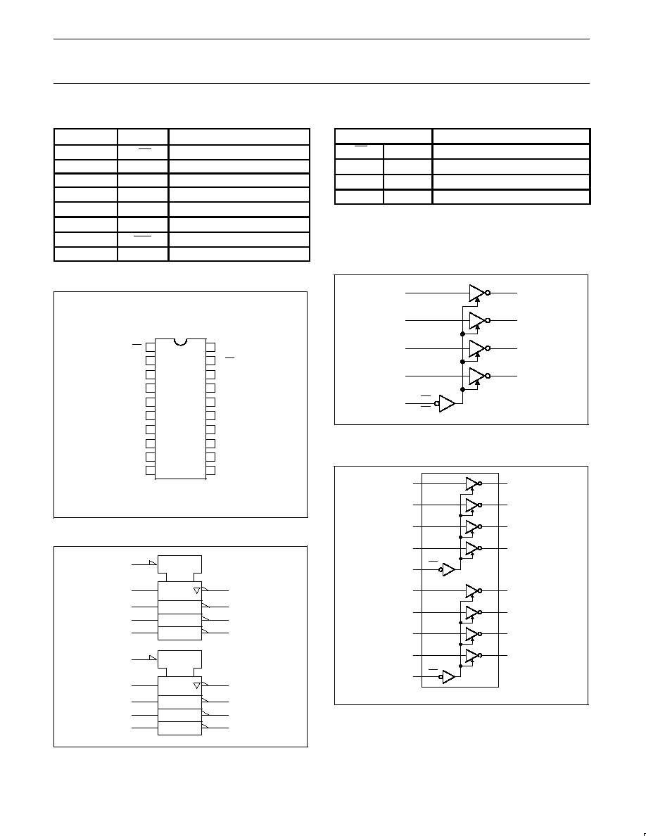
PIN CONFIGURATION
1
2
3
4
5
6
7
8
9
10
11
12
13
14
15
16
17
18
19
20
1OE
1A0
2Y0
1A1
2Y1
1A2
2Y2
1A3
2Y3
1Y3
GND
2A2
1Y2
2A1
1Y1
2A0
1Y0
2OE
VCC
2A3
SV00212
LOGIC SYMBOL (IEEE/IEC)
SV00611
18
16
14
12
2
4
6
8
EN
1
9
7
5
3
11
13
15
17
EN
19
FUNCTION TABLE
INPUTS
OUTPUT
nOE
nA
n
nY
n
L
L
H
L
H
L
H
X
Z
H = HIGH voltage level
L
= LOW voltage level
X = Don't care
Z = High impedance OFF-state
LOGIC SYMBOL
SV00608
1A 0
2A 0
2
17
1A 1
2A 1
4
15
1A 2
2A 2
6
13
1A 3
2A 3
8
11
1OE
2OE
1
19
1Y 0
2Y 0
18
3
1Y 1
2Y 1
16
5
1Y 2
2Y 2
14
7
1Y 3
2Y 3
12
9
FUNCTIONAL DIAGRAM
SV00610
2Y 0 3
2Y 1 5
2Y 2 7
2Y 3 9
2A 0
17
2A 1
15
2A 2
13
2A 3
11
2OE
19
1Y 0 18
1Y 1 16
1Y 2 14
1Y 3 12
1A 0
2
1A 1
4
1A 2
6
1A 3
8
1OE
1
Philips Semiconductors
Product specification
74LVC240A
Octal buffer/line driver with 5-volt
tolerant inputs/outputs; inverting (3-State)
1998 May 20
4
RECOMMENDED OPERATING CONDITIONS
SYMBOL
PARAMETER
CONDITIONS
LIMITS
UNIT
SYMBOL
PARAMETER
CONDITIONS
MIN
MAX
UNIT
V
CC
DC supply voltage (for max. speed performance)
2.7
3.6
V
V
CC
DC supply voltage (for low-voltage applications)
1.2
3.6
V
V
I
DC Input voltage range
0
5.5
V
V
O
DC Output voltage range; output HIGH or LOW
state
0
V
CC
V
O
DC output voltage range; output 3-State
0
5.5
T
amb
Operating ambient temperature range in free-air
40
+85
°
C
t
r
, t
f
Input rise and fall times
V
CC
= 1.2 to 2.7V
V
CC
= 2.7 to 3.6V
0
0
20
10
ns/V
ABSOLUTE MAXIMUM RATINGS
1
In accordance with the Absolute Maximum Rating System (IEC 134)
Voltages are referenced to GND (ground = 0V)
SYMBOL
PARAMETER
CONDITIONS
RATING
UNIT
V
CC
DC supply voltage
0.5 to +6.5
V
I
IK
DC input diode current
V
I
t
0
50
mA
V
I
DC input voltage
Note 2
0.5 to +6.5
V
I
OK
DC output diode current
V
O
u
V
CC
or V
O
t
0
"
50
mA
V
O
DC output voltage; output HIGH or LOW state
Note 2
0.5 to V
CC
+0.5
V
V
O
DC output voltage; output 3-State
Note 2
0.5 to 6.5
V
I
O
DC output source or sink current
V
O
= 0 to V
CC
"
50
mA
I
GND
, I
CC
DC V
CC
or GND current
"
100
mA
T
stg
Storage temperature range
65 to +150
°
C
Power dissipation per package
P
TOT
plastic mini-pack (SO)
above +70
°
C derate linearly with 8 mW/K
500
mW
plastic shrink mini-pack (SSOP and TSSOP)
above +60
°
C derate linearly with 5.5 mW/K
500
mW
NOTES:
1. Stresses beyond those listed may cause permanent damage to the device. These are stress ratings only and functional operation of the
device at these or any other conditions beyond those indicated under "recommended operating conditions" is not implied. Exposure to
absolute-maximum-rated conditions for extended periods may affect device reliability.
2. The input and output voltage ratings may be exceeded if the input and output current ratings are observed.
Philips Semiconductors
Product specification
74LVC240A
Octal buffer/line driver with 5-volt
tolerant inputs/outputs; inverting (3-State)
1998 May 20
5
DC ELECTRICAL CHARACTERISTICS
Over recommended operating conditions voltages are referenced to GND (ground = 0V)
LIMITS
SYMBOL
PARAMETER
TEST CONDITIONS
Temp = -40
°
C to +85
°
C
UNIT
MIN
TYP
1
MAX
V
HIGH level Input voltage
V
CC
= 1.2V
V
CC
V
V
IH
HIGH level Input voltage
V
CC
= 2.7 to 3.6V
2.0
V
V
LOW level Input voltage
V
CC
= 1.2V
GND
V
V
IL
LOW level Input voltage
V
CC
= 2.7 to 3.6V
0.8
V
V
CC
= 2.7V; V
I
= V
IH
or V
IL
; I
O
= 12mA
V
CC
*
0.5
V
O
HIGH level output voltage
V
CC
= 3.0V; V
I
= V
IH
or V
IL
; I
O
= 100
µ
A
V
CC
*
0.2
V
CC
V
V
OH
HIGH level output voltage
V
CC
= 3.0V; V
I
= V
IH
or V
IL;
I
O
= 18mA
V
CC
*
0.6
V
V
CC
= 3.0V; V
I
= V
IH
or V
IL;
I
O
= 24mA
V
CC
*
0.8
V
CC
= 2.7V; V
I
= V
IH
or V
IL
; I
O
= 12mA
0.40
V
OL
LOW level output voltage
V
CC
= 3.0V; V
I
= V
IH
or V
IL
; I
O
= 100
µ
A
GND
0.20
V
V
CC
= 3.0V; V
I
= V
IH
or V
IL;
I
O
= 24mA
0.55
I
Input leakage current
2
V
= 3 6V; V = 5 5V or GND
"
0 1
"
5
µ
A
I
I
Input leakage current
2
V
CC
= 3.6V; V
I
= 5.5V or GND
"
0.1
"
5
µ
A
I
OZ
3-State output OFF-state current
V
CC
= 3.6V; V
I
= V
IH
or V
IL
; V
O
= 5.5V or GND
0.1
"
10
µ
A
I
off
Power off leakage current
V
CC
= 0.0V; V
I
or V
O
= 5.5V
0.1
"
10
µ
A
I
CC
Quiescent supply current
V
CC
= 3.6V; V
I
= V
CC
or GND; I
O
= 0
0.1
10
µ
A
I
CC
Additional quiescent supply current
per input pin
V
CC
= 2.7V to 3.6V; V
I
= V
CC
0.6V; I
O
= 0
5
500
µ
A
NOTES:
1. All typical values are at V
CC
= 3.3V and T
amb
= 25
°
C.
2. The specified overdrive current at the data input forces the data input to the opposite logic input state.
AC CHARACTERISTICS
GND = 0V; t
r
= t
f
v
2.5ns; C
L
= 50pF; R
L
= 500
; T
amb
= 40
°
C to +85
°
C.
LIMITS
SYMBOL
PARAMETER
WAVEFORM
V
CC
= 3.3V
±
0.3V
V
CC
= 2.7V
V
CC
= 1.2V
UNIT
MIN
TYP
1
MAX
MIN
MAX
TYP
t
PLH
t
PHL
Propagation delay
1A
n
to 1Y
n
;
2A
n
to 2Y
n
1, 3
1.5
3.5
6.5
1.5
7.5
16.0
ns
t
PZH
t
PZL
3-State output enable time
1OE to 1Y
n
;
2OE to 2Y
n
2, 3
1.5
4.3
8.0
1.5
9.0
19.0
ns
t
PHZ
t
PLZ
3-State output disable time
1OE to 1Y
n
;
2OE to 2Y
n
2, 3
1.5
3.7
7.0
1.5
8.0
17.0
ns
NOTE:
1. Unless otherwise stated, all typical values are at V
CC
= 3.3V and T
amb
= 25
°
C.